-
Paper Information
- Previous Paper
- Paper Submission
-
Journal Information
- About This Journal
- Editorial Board
- Current Issue
- Archive
- Author Guidelines
- Contact Us
American Journal of Materials Science
p-ISSN: 2162-9382 e-ISSN: 2162-8424
2014; 4(3): 133-138
doi:10.5923/j.materials.20140403.03
Characterization Studies on Field Assisted-Electrostatic Spray Pyrolysis Deposition of Zns Thinfilms for Optoelectronic Applications
 Abstract
 Reference
 Full-Text PDF
 Full-text HTML
Adama Kenneth K. , Alu Noble , Iwok Unwana U. , Abdullahi Zakari , Bwamba Jonah A. , Egba Augustine C. , Oberafo Anthony A.
Physics Advanced Laboratory, Sheda Science & Technology Complex (SHESTCO), P.M.B 186, Garki – Abuja
Correspondence to: Adama Kenneth K. , Physics Advanced Laboratory, Sheda Science & Technology Complex (SHESTCO), P.M.B 186, Garki – Abuja.
| Email: |  |
Copyright © 2014 Scientific & Academic Publishing. All Rights Reserved.
We investigated the properties of zinc sulphide thinfilms deposited using a field assisted electrostatic spray pyrolysis deposition apparatus at an optimized substrate temperature, time, pressure and flowrate of 300oC, 10minutes, 1atm and 0.5ml/min respectively. The ZnS thin films were there-after annealed at 350oC for 3hours. The influence of process parameters on the properties of the ZnS thinfilms were investigated using x-ray diffractometry, uv-spectrophotometry and profilometry. The morphology of the films and the nano-mechanical properties of the optimized thinfilms were also investigated using nano-indentation technique. The optimized films obtained were transparent, homogeneous, uniformly dispersed with an average surface thickness of 500nm and roughness of 206.65nm. It had a polycrystalline hexagonal structure and a relative optical transmittance in the visible spectrum of more than 60%. The morphology of the film revealed a highly oriented nanostructure composed of uniformly and evenly distributed pore materials. The pores; inevitably influencing the optical properties of the films. The films would find applications in dielectric filters, electroluminescent and solar cells devices.
Keywords: Field assisted, Electrostatic spray pyrolysis, Zinc sulphide films, Characterization, Optoelectronics
Cite this paper: Adama Kenneth K. , Alu Noble , Iwok Unwana U. , Abdullahi Zakari , Bwamba Jonah A. , Egba Augustine C. , Oberafo Anthony A. , Characterization Studies on Field Assisted-Electrostatic Spray Pyrolysis Deposition of Zns Thinfilms for Optoelectronic Applications, American Journal of Materials Science, Vol. 4 No. 3, 2014, pp. 133-138. doi: 10.5923/j.materials.20140403.03.
Article Outline
1. Introduction
- Zinc sulphide thinfilms are used in several optoelectronic devices which include UV light emitting diodes, blue light emitting diodes, emissive flat screens, electroluminescent devices and antireflection coatings in solar cell technology [1-3]. Being a known semi-conductor and with its wide band gap, it can be used as a transparent material in the visible light region as dielectric filters. ZnS occurs mainly in two phases which are α-phase and β-phase [1].Different techniques have been employed in the preparation of ZnS thinfilms. These include thermal decomposition, sol-gel, precipitation, forced hydrolysis, sputtering, vacuum evaporation, spin coating, electrodeposition, chemical bath deposition (CBD) and spray-based (aerosol) production [4-9]. Amongst these methods, spray pyrolysis enables both kinetic (nucleation/ growth) and thermodynamic control through the fine tuning of deposition parameters giving rise to enhanced tailored materials for specific applications [10-11].The technique of field assisted electrostatic spray pyrolysis of ZnS thinfilms offers the possibility of depositing layered films and films with homogeneous composition gradients over a large area of the substrate through changing of the composition of the spray solution and deposition parameters [10-16]. This method which is a one –step can be used to produce thinfilms which are highly homogeneous, uniformly shaped and of high purity in large quantities [17]. It is a relatively cheap and dry deposition process with adequate control over deposition rate [8].In spite of the fact that ZnS has been extensively investigated in the light of its structural and optical properties, many issues still remain to be understood on the applicability of the films in optoelectronics.In this paper, production of homogeneous and uniformly dispersed ZnS thinfilms is undertaken using field assisted electrostatic spray pyrolysis deposition apparatus. The influence of the optimized molar concentrations of the zinc acetate and thiourea precursors on the ZnS thinfilms produced is studied. X-ray diffraction, uv-visible spectroscopy, nano-indentation studies and profilometry techniques are used to evaluate the influence of the process parameters on the properties of the ZnS thinfilms.
2. Experimental
- The ZnS thinfilms were deposited on glass slides by the spray pyrolysis technique described in previous works [5-7]. The temperature at which deposition was carried out was varied using 300°C, 350°C and 400°C respectively to ascertain the influence of process temperature and the optimized temperature was found to be 300°C. In the same manner, the deposition time was varied from 5min, 10mins and 20mins respectively and it was observed that uniformly deposited films was obtained at 10minutes deposition time. The deposition process was carried out at an optimized substrate temperature, time, pressure and flowrate of 300℃, 10minutes, 1atmoshphere, and 0.5ml/min respectively followed by annealing at 350°C in open air for 3hrs, taking into effect the influence of the following parameters on the film thickness: the spray nozzle- substrate distance, the substrate temperature, the concentration of the precursor solution, and the amount of sprayed precursor solution.Essentially, the chemical reaction in the formation of ZnS thinfilms from Zinc acetate and thiourea in an aqueous medium is given as follows:
 | (1) |
 | (2) |
 | (3) |
 | (4) |
3. Results and Discussions
3.1. Structural Analysis
- The X-ray diffractogram of ZnS thinfilms obtained by the field assisted electrostatic spray pyrolysis deposition technique at the three operating temperatures of 300°C, 350°C and 400°C process parameters is shown in Figure 1 below.
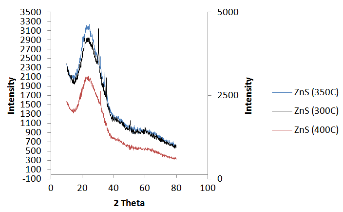 | Figure 1. X-ray diffraction pattern of ZnS thinfilms deposited at 300C, 350C and 400C and annealed at 350C process parameter |
3.2. Optical Properties
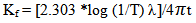
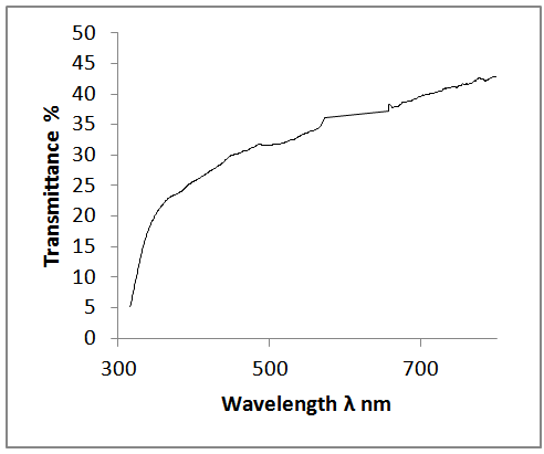
- Figure 2 and Figure 3 above shows the transmittance and absorbance spectra in the wavelength range of 200-900nm for the ZnS thinfilms deposited at the optimized process parameters of temperature of 300°C and annealed at 350℃ for 3hours. From the figures, it was observed that at the optimized process parameters, there was an improvement in the optical transmittance as well as absorbance of the thinfilms which were attributable to the surface thickness of the films. Generally, the transmittance of the deposited thinfilms increased with wavelength between 350nm to 800nm which indicated that the region of absorbance lies below the wavelength. It was also observable that as the ZnS thinfilms were annealed, there was a general increase in the average transmittance and absorbance. This was because of the decrease in the defect density caused by the annealing process. The relative optical transmittance in the uv-vis spectrum was observed to be more than 60% indicative of a good material for optoelectronic devices. The ZnS thinfilms had excellent absorption at relatively short wavelength regions. However, it was observed that increasing the wavelength resulted in decreased absorption. In all cases, the absorption coefficient α and absorption index (extinction coefficient) Kf were obtained from the transmittance, T, as follows.
 | (5) |
 | Figure 2. Optical transmittance spectra of the ZnS thinfilm |
 | Figure 3. Optical absorbance spectra of the ZnS thinfilm |
 | (6) |
3.3. Surface Profilometry
- The average surface thickness and roughness of the optimized ZnS thinfilms was obtained using a Veeco Dektak 150 Stylus Surface Profiler. It was observed that at the optimized process condition, the average surface thickness and roughness were 500nm and 206.65nm respectively. The films were observed to be homogeneous and uniformly dispersed on the substrates.
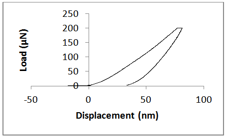
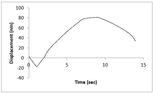
3.4. Nano-indentation Morphology
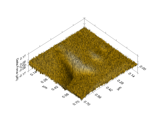
- The nanographs of the deposited ZnS thinfilms show that the films have highly oriented nanostructures. The pores inevitably influenced the optical properties of the thinfilm. The morphology of the film revealed a highly oriented nanostructure composed of uniformly and evenly distributed pore materials. The films showed a flat, dense, evenly and uniformly distributed thin film surface. This is shown in figures 4, 5 and 6 below.
 | Figure 4. Nanograph of ZnS sample annealed at 350°C |
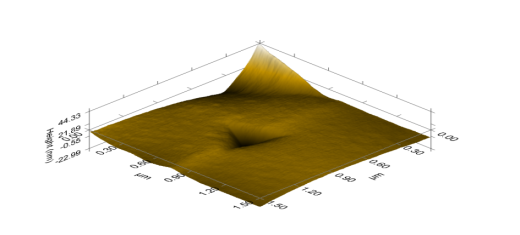 | Figure 5. ZnS annealed 3D morphological depth indentation of thinfilm |
 | Figure 6. Unannealed ZnS nanograph of sample deposited at 300C |
 | Figure 7. Actuation- Displacement graph for unannealed ZnS sample |
 | Figure 8. Constant strain rate for the unannealed ZnS samples |
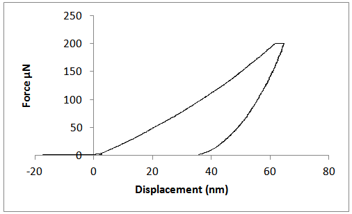 | Figure 9. Actuation- Displacement graph for annealed ZnS sample |
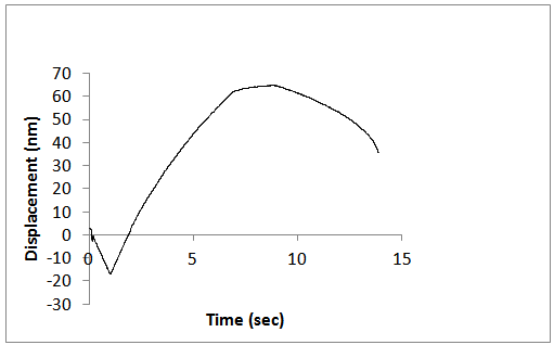 | Figure 10. Constant strain rate for the annealed ZnS samples |
4. Conclusions
- Transparent, homogeneous and uniformly dispersed ZnS thinfilms were successfully deposited using field assisted – electrostatic spray pyrolysis apparatus at the optimized substrate temperature, time, pressure, and flowrate of 300℃, 10minutes, 1atmosphere and 0.5ml/min respectively. Polycrystalline ZnS films with reference to the more pronounced (111) plane at 2Θ peak position of 30.2335˚ was obtained at the deposition temperature of 300℃ and annealed temperature of 350℃ for 3hours. The nano- mechanical indentation studies of the thinfilms showed the films have highly oriented nanostructures whose influences on the optical properties of the films are significant. The films showed a flat, dense, evenly and uniformly distributed surface. The optical properties of the thinfilms showed an improvement in optical transmittance occasioned by the decrease in the defect density due to the annealing process. Relatively, optical transmittance in the uv-vis spectrum was more than 60% with surface properties of thickness and roughness obtained as 500nm and 206.65nm respectively. Estimation of the optical energy gap of the thin films was observed to be 3.436eV. The films can be utilized in dielectric filters, electroluminescent and solar cell devices.
ACKNOWLEDGEMENTS
- The authors wish to acknowledge the Management of Sheda Science and Technology Complex (SHESTCO), Abuja for making available the equipment used in this research.