-
Paper Information
- Next Paper
- Previous Paper
- Paper Submission
-
Journal Information
- About This Journal
- Editorial Board
- Current Issue
- Archive
- Author Guidelines
- Contact Us
American Journal of Materials Science
p-ISSN: 2162-9382 e-ISSN: 2162-8424
2014; 4(3): 127-132
doi:10.5923/j.materials.20140403.02
Characterization of CZTS Absorbent Material Prepared by Field-Assisted Spray Pyrolysis
 Abstract
 Reference
 Full-Text PDF
 Full-text HTML
Bwamba Jonah A. , Alu Noble , Adama Kenneth K. , Abdullahi Zakari , Iwok Unwana U. , Egba Augustine C. , Oberafo Anthony A.
Physics Advanced Laboratory, Sheda Science & Technology Complex, P. M. B. 181, Garki - Abuja
Correspondence to: Bwamba Jonah A. , Physics Advanced Laboratory, Sheda Science & Technology Complex, P. M. B. 181, Garki - Abuja.
| Email: |  |
Copyright © 2014 Scientific & Academic Publishing. All Rights Reserved.
In this work we deposited Cu2ZnSnS4 (CZTS) thin films on soda-lime glass (SLG) substrate using electrostatic field-assisted low-cost spray pyrolysis technique. The precursor solution, consisting of Cu2Cl, ZnCl2, SnCl4 and thiourea at optimized concentrations, was sprayed onto a heated SLG substrate at a flow rate of 0.33ml/min. Spray deposition was carried out at substrate temperatures of 300℃ with varying precursor concentrations. After deposition of the CZTS thin films, the films were annealed at a temperature of 350℃ in argon atmosphere for 60minutes. The Structural characterization of the annealed CZTS film was carried out by X-ray diffraction (XRD) while the film thickness, micrograph, optical and electrical properties were measured using Veeco Dektak 150 Stylus profiler, Carl Zeiss Optical interference microscope, UV-Vis-NIR spectroscopy and four point probe techniques respectively. The result obtained from the XRD showed a peak at the 2θ position of 31.7200° with a FWHM of 0.3600° and d-spacing of 2.81863Å. The annealed CZTS films exhibited excellent polycrystalline orthorhombic structure from XRD measurements. The average sheet resistance of the films is in the region of 7.264X10⁷ Ωsq from a thickness of 100nm under dark conditions. The film micrograph obtained at 1,000x using the Carl Zeiss optical interference microscope showed light agglomeration of grains and voids of sparcely dispersed films.
Keywords: Spray Pyrolysis, Thin films, CZTS
Cite this paper: Bwamba Jonah A. , Alu Noble , Adama Kenneth K. , Abdullahi Zakari , Iwok Unwana U. , Egba Augustine C. , Oberafo Anthony A. , Characterization of CZTS Absorbent Material Prepared by Field-Assisted Spray Pyrolysis, American Journal of Materials Science, Vol. 4 No. 3, 2014, pp. 127-132. doi: 10.5923/j.materials.20140403.02.
Article Outline
1. Introduction
- Copper zinc tin sulfide (CZTS) is an emerging thin film for solar photovoltaic absorber material and is composed of earth abundant, nontoxic, and cheap materials. It is a semiconductor with a direct band gap of about 1.5 eV and an absorption coefficient of 104 cm−1 [1]. Therefore, a thickness of 1-2 𝜇m is sufficient for absorbing the solar radiation. It is a good substitute for copper indium gallium selenide (CIGS) solar photovoltaic absorber, which is composed of scarce, expensive and relatively toxic materials. A record efficiency of 20.3% has been recorded for CIGS solar cells [2]. There are challenges associated with stability of the solar cells developed using CZTS and CIGS. CZTS and CIGS solar cells have similar challenges in terms of research directions [3]. The highest reported efficiency of CZTS solar cell is ~11.1% [4], in order to commercialize CZTS thin film solar cell, its efficiency needs to be enhanced. The efficiency of a material for PV applications can be greatly influenced by the method chosen to fabricate the semiconductor material. Different methods for synthesizing CZTS absorber materials have been reported in the literature [5–18]. The methods include thermal evaporation [5], sputtering from metal targets (layer by layer) [6], sputtering from sulfide or composite targets [7], pulsed-laser depositions [8], chemical methods such as sol-gel [9], electrodeposition [10], and nanocrystals synthesis [11]. Among the physical vapor deposition techniques, sputtering is widely used in industry.The synthesis of CZTS thin films by deposition of precursor solutions using spray pyrolysis technique in ambient environment was reported by some authors [32]. They used CuCl2, ZnCl2, SnCl4 and thiourea at suitable concentrations in deionized water/ethanol solvent mixture as precursor solution to prepare CZTS thin films that was sprayed onto a heated SLG substrate. Spray pyrolysis proved to be a suitable method for the deposition of large area metal oxide, spinel oxide, chalcogenide and different sulphide films [27, 28]. The process is already widely applied and is attractive for the deposition of low-cost thin film photovoltaic solar cells [29]. The technique offers the possibility of depositing layered films and films with composition gradients throughout the thickness of the film by changing the composition of the spray solution and deposition parameters.During the spray pyrolysis deposition process, a precursor aerosol is sprayed towards the substrate. The component in the precursor aerosol react to form a new chemical compound on the substrate surface and usually some byproducts that should vapourised in the open atmosphere. The properties of the deposited films depend on the precursors’ solution, qualitative composition, spraying rate, substrate temperature, ambient atmosphere, carrier gas, droplet size and the cooling rate after deposition. The film thickness is influenced by the spray nozzle distance, the substrate temperature, the concentration of the precursor and the amount of the sprayed precursor solution. The thin film formation depends on the reactant/solvent evaporation and on the process of droplet landing. The ideal deposition condition is considered when the solvent is completely removed at the moment the droplet approaches the substrate where the chemical reaction occurs [30]. The reactant molecules undergo process of absorption, surface diffusion and chemical reaction, leading to nucleation and layer growth while volatile byproducts evaporate and diffuse away from the surface [31]. Several authors have studied the effect of the substrate temperature and the spray duration on the crystallinity of CZTS thin films. The best crystallinity was obtained at the substrate temperature 613℃ and a preferential orientation along [112] plane was observed with the films [22]. The effect of the substrate temperature and the pH value as well as the compositions of the precursor solution on the crystallinity and the morphology of the CZTS material was also investigated by other authors. Their results showed that the CZTS material with good crystallinity was obtained at the substrate temperature in the range of 370-410℃ with the precursor solution pH = 4.5. But impurities such as ZnS were observed besides the CZTS compound [22, 23, 24]. Prabhakar and Nagaraji used ultrasonic spray pyrolysis technique to deposit CZTS thin films on a SLG substrate. The films with kesterite structure were obtained at 613 K, consistent with the results reported by others [25].In this work, we have developed thin-film CZTS by atomic pulverization technique called "spray pyrolysis". This method has found great success in recent years since it has become an integral part in the industrial process for cell preparation on a large scale. The CZTS thin layers are deposited on heated glass substrates prepared from an aqueous solution containing copper ions, zinc, tin and sulfur at optimized temperatures. The structural, electrical, film thickness, surface morphology and optical properties of the annealed thin films were analyzed by X-ray diffraction (XRD), four point-probe technique, Veeco Dektak 150 stylus profiler, Carl Zeiss optical interference microscope and UV-Vis-NIR spectroscopy respectively.
2. Methodology
- The CZTS thin films were deposited by the spray pyrolysis technique on SKYTEC ISO 9001:2000 soda glass substrates of slide dimension 25.4x 76.2mm (1'x3'), precleaned and thickness of 1.0mm-1.2mm, at a substrate temperature of 300°C and deposition time of 16 min and thereafter annealed at 350℃ in an atmosphere of Ar gas for 60 min so as to improve the crystallinity of the thin films. The spray pyrolysis set up used in the study consisted of a precursor delivery system (pump), an atomizing nozzle, a high tension or voltage source, a substrate heater and a temperature controller. The nozzle specification is gauge 24 hypodermic needle with nominal outer diameter of 0.02225 inches (0.5652mm) and nominal inner diameter of 0.01225 inches (0.311mm) and nominal wall thickness of 0.005 inches (0.1270mm). The glass substrates used for the thin film preparation were washed with 5% HNO3 and then rinsed with distilled water, ethanol and acetone in that order. The thin film layers of CZTS were prepared from aqueous solutions consisting CuCl2 (0.1 M), ZnCl2 (0.1M), SnCl4 (0.1M) and thiourea (0.8M) in a solvent mixture of acetic acid, distilled water and ethanol in the ratio of 2:3:5 without additional sulfurization. The solution was sprayed at a flow rate of 0.33 ml / min. The nozzle-substrate distance was fixed at 20 cm. The precursor mixture was then atomized electro-statically at a high voltage of about 17kV. The absorbance of the films was determined from the transmittance data obtained from the UV-Vis-NIR Spectrophotometer (Avantes) in the wavelength ranging from 250nm to 850nm. The structural study of the annealed films was obtained by means of the PANalytical X’Pert PRO MPD X-ray diffraction PW3040/60 system using Cukα monochromatic radiation. The wavelength accelerating voltage and current were 1.5406Ǻ, 45KV and 40mA, respectively. The intensity of the rays was measured at Bragg’s 2θ angle from a start angle of 10° to an end angle of 100°, step size of 0.1°, acquisition scan step time of 249.5550sec and was of a continuous scan type. The result was displayed as the scan spectra on a real time computer connected to the XRD system. The crystallinity and other important parameters were determined from the X-ray diffraction analysis using the system’s software. The microstructure of the annealed films was obtained using the Carl Zeiss optical interference microscope.
3. Results and Discussion
3.1. Structural Characterization
- The XRD profile of the deposited and annealed CZTS thin film is shown in figure 1 below. The XRD analysis spectra showed presence of one pronounced peak at 2θ position of 31.7200°. The phase analysis revealed peaks corresponding to the (312) planes, which are characteristics of the CZTS phases. The obtained structural parameters from the analysis are summarized in table 1. It was observed that the films obtained were highly preferentially oriented in the (312) plane which exhibits an orthorhombic crystal structure. The observed diffraction spectrum was found to be in agreement with the International Center for Diffration Data (ICDD) reference values. The XRD software’s Scherrer calculator was used to evaluate the spectra’s crystallite size (Ǻ) and was found to be 9Ǻ (0.9nm) and 14.600% respectively from a Full Width at Half Maximum (FWHM) of 0.3600°, height of peak of 4764.25 (cts) and d-spacing (Ǻ) of 2.81863. Typical XRD pattern of the sprayed CZTS films is shown in figure 1.
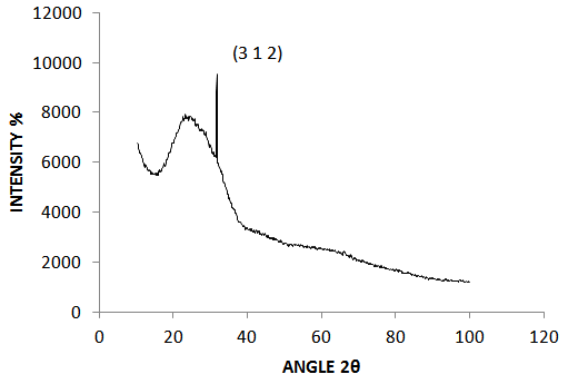 | Figure 1. X-ray diffraction pattern of Cu2ZnSnS4 annealed at a temperature of 350℃ |
|
3.2. Optical Characterization
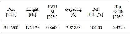
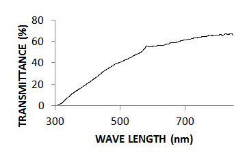
- The optical absorption studies of the annealed CZTS thin films in the wave length range of 250nm – 850nm was investigated using avantes UV-Vis-NIR unpolarized single beam spectrophotometer. It was found that the absorption peak of the thin film occurs at 260 nm, unlike that of bulk samples which peaked at about 320 nm, thus clearly indicating a widening of bandgap. The variations of transmittance and absorbance with wavelength are shown in figures 2 and 3 respectively. These spectra revealed that the annealed CZTS thin films have a high absorbance of light in the visible region indicating applicability as an absorbing material. The absorption coefficient with wavelength plot in figure 4 shows the variation of absorption coefficient [(αhν)2] versus photon energy [hν]. The extrapolation of this curve to zero absorption coefficient (i.e. α = 0) gives the bandgap energy to be 1.54eV for the annealed CZTS thin film which is consistent with that reported in earlier results [19, 20]. This is close to the optimal bandgap required for solar cells and therefore the film is considered to be suitable for use as an absorbent material for photovoltaic applications [21].
 | Figure 2. Represents UV-VIS Transmittance spectrum of the annealed CZTS thin film |
 | Figure 3. Represents UV-VIS absorption spectrum of the annealed CZTS thin film |
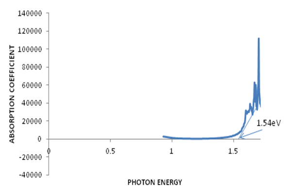 | Figure 4. Absorption coefficient versus photon energy for bandgap determination of CZTS thin film |
3.3. Surface Profilometry / Electrical Properties
- The average film thickness of the annealed CZTS thin films was obtained using a Veeco Dektak 150 Stylus Surface Profiler. It was observed that at the optimized process condition, the average surface thickness was 100nm. This film thickness was further employed to determine the sheet resistance of the film using the four point probe method. This measured to give a sheet resistance of 7.26 x 10⁷ Ωsq in dark conditions.
3.4. Surface Morphology
- The micrograph of the CZTS thin film obtained from the Carl Zeiss Optical interference microscope at 1,000x magnification is shown in figure 5. It was observed that the films did not have even or uniform microstructure of CZTS films. There were pores and light agglomeration of grain observed on the thin film and this was observed to influence the optical and structural properties of the CZTS thin films. Voids around the sparsely dispersed films were also observed on the micrograph which in turn influenced the resistivity of the material.
 | Figure 5. Optical Microscope micrograph of CZTS thin film |
4. Conclusions
- In this study CZTS thin films were successful deposited on soda lime glass at 300℃ using field assisted chemical spray pyrolysis technique. Thereafter the as-deposited thin films were annealed at 350℃ in argon atmosphere to enhance its crystallinity. At the operating process parameter of deposition and annealing, the structural analysis using XRD showed the presence of one pronounced peak at 2θ position of 31.72o which corresponded to the (3 1 2) planes characteristics to the CZTS phase. The films were found to be preferentially oriented and exhibited orthorhombic crystal structure from analysis. The micro-structural analysis show pores and light agglomeration of grain observed on the thin film and this was observed to influence the optical and structural properties of the CZTS thin films. It was noted that CZTS thin film photovoltaic absorber layers can be deposited through solution growth technique for quaternary material and the four elements which are used are better binded through solution deposition technique. The optical properties of the CZTS thin films deposited showed high absorption in the visible region of the spectrum and also with a direct bandgap of 1.54eV. This is close to the optimum bandgap required for a solar cell thus indicating CZTS is a promising material for thin film solar cell applications [21]. The XRD analyses indicated that the deposited films have nano-crystalline structure that gave a film thickness of 100nm using the Veeco Dektak 150 stylus profiler. This film thickness was used to obtain an average sheet resistance of 7.264X10⁷ Ωsq under dark conditions. The high value of resistivity may be attributed due to nano crystsllinity or amorphous form of the film, grain boundary discontinuities and the presence of surface states [26]. The prepared CZTS films’ structural and optical properties have shown it to be suitable for absorber layers in efficient thin film solar cells applications. So, this method is not only low-cost, but can also be used for large area production instead of expensive and complicated equipment.
ACKNOWLEDGEMENTS
- The authors of this research work wish to acknowledge the management of Sheda Science and Technology Complex, Abuja for making available the equipment used in this research.