-
Paper Information
- Next Paper
- Previous Paper
- Paper Submission
-
Journal Information
- About This Journal
- Editorial Board
- Current Issue
- Archive
- Author Guidelines
- Contact Us
Science and Technology
p-ISSN: 2163-2669 e-ISSN: 2163-2677
2013; 3(2A): 32-40
doi:10.5923/s.scit.201301.06
Structural and Electronic Properties of Si Nanostructures
 Abstract
 Reference
 Full-Text PDF
 Full-text HTML
Sana Kausar, Shirish Joshi
Dept. of Physics, Govt. M.V.M. College, Bhopal, India
Correspondence to: Sana Kausar, Dept. of Physics, Govt. M.V.M. College, Bhopal, India.
| Email: |  |
Copyright © 2012 Scientific & Academic Publishing. All Rights Reserved.
The stability and electronic structure of a single monatomic Silicon nanowire has been studied using density functional theory. The Si nanowire undergoes two structural rearrangements when it undergoes compression, i.e., zigzag configurations. Cohesive energy and bond length of Si nanostructures (chains and monolayers) are examined by using Generalized geometry approximation and Local density approximation. The relation between low dimensional 1D structure (chain) to high dimensional 3D bulk Si is estimated.
Keywords: GGA, nanowire,castep and LDA
Cite this paper: Sana Kausar, Shirish Joshi, Structural and Electronic Properties of Si Nanostructures, Science and Technology, Vol. 3 No. 2A, 2013, pp. 32-40. doi: 10.5923/s.scit.201301.06.
1. Introduction
- Nanowire-based photovoltaic structures are currently of great interest due to their potential to reduce manufacturing costs while allowing keeping good efficiencies and device lifetimes. Nanowires have two quantum-confined dimensions and one unconfined dimension. Hence, the electrical conduction of nanowires is different from their bulk counterpart. In nanowires, electronic conduction takes place due to bulk conduction and tunneling mechanism. However, due to their high density of electronic state, dependency of band gap on diameter, enhanced surface scattering of phonons s and electron, increased excitation binding energy, high surface to volume ratio and large aspect ratio, nanowires of metals and semiconductor exhibit unique electrical, magnetic, optical, thermoelectric and chemical properties in comparison to their bulk counterparts[2]. Due to interesting properties of nanowires it has lot of applications in the fields of electronics, optics, magnetic medium, thermo electronic, sensor devices etc (Tonucci et al 1992; Whitney et al 1993). The fundamental issues in building a nanowires are ability to control the scale (size) of the system, ability to obtain the required composition (not just the average composition - but details such as defects, concentration gradients, etc), ability to control the modulation dimensionality and during the assembly of the nano-sized building blocks, one should be able to control the extent of the interaction between the layers as well as the architecture of the material itself[1].Many theoretical and experimental studied has already been carried out to study the structural and electronic properties of nanaowires and their application. Erik C. Garnett et.al studied Nanowire Solar Cells[3] .B.Lassen et.al studied the Electronic structure of free-standing InP and InAs nanowires[4]. Jaya Sarkar et al.[2] studied the properties, applications and synthesis of nanowire via porous anodic aluminium oxide template. Sánchez-Portal et al.[5] predicted the spinning zigzag shape of monatomic gold wires, and explained current transmission electron microscopy (TEM) results[6]. Relatively a few studies have focused on other metal nanowires. The expectation that Si nanowires should also have unique properties is the motivation of this work. Rubio et.al[7] took the first step to simulate the one dimensional Al atoms chains in BN nanotubes and showed interaction effects. Jin-Cheng Zheng et al.[11] perform first principles calculations to address the questions of structure and stability, as well as the evolution of electronic structure of an infinite Al monatomic wire under compression. In present study the effects of density functional on cohesive energy and bond length of Si nanowires along[1 1 1] direction is analyzed and discuss the link from low dimensional 1D structure (chain) to high dimensional 3D bulk structure of Si metal.
2. Method of Computations
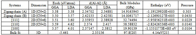
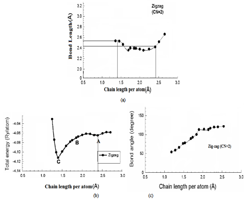
- Total energy package, CASTEP[9,10], has been used to carry out the calculations of band structure and examine the density functional effect of the binding energy and bond length of Si nanowires. We performed systematic studies on Si nanostructures ranging from atomic chains (1D), monolayers (2D) to bulk Si(3D) with generalized geometry approximation pw91[11] and local density approximation using an ultrasoft pseudopotential[12]. Special k points are generated by the Monkhorst-Pack scheme[13]. The (1x1x40) k points are used for atomic chains, and Monkhorst-Pack k point with spacing of 0.05Å-1 are generated for monolayers and bulk Si.The wire calculations were performed by applying generalized geometry approximation method within the local density functional theory. The exchange correlation potential has been approximated by Generalized Geometry Approximation using Perdew Burke Ernzerhof exchange correlation functional both for spin-polarized and spin-unpolarized cases. For partial occupancies, we use Gaussian smearing method. The adopted smearing width is 0.1 eV for the atomic relaxation and 0.05 for the accurate band structure analysis and density of states calculations, here total energy / atom convergence tolerance is 0.1000E-05 eV. During the self-consistent iterations, 40 special k-points in the Brillouin zone are used to calculate the screen potential and charge density. The chain configurations of Si atoms studied are the monoatomic zigzag chain and di-atomic chain, as shown in Fig. 1(A) and Fig.1(B). We have performed first-principles plane wave calculations[11,12] within DFT[13] using ultrasoft pseudopotentials[12,14]. The supercell concept is used to generate a three-dimensional periodic tetragonal lattice with chains along the z axis separated in the x and y directions. These separations between the chains are as wide as 4Å, which is found to be large enough to separate the chains, thereby effectively removing inter-chain interactions. The lattice constants of the tetragonal super cell in the x-y plane are taken as asc=bsc=26 Å and csc=9.406 Å along the z axis. For the double unit cell calculations, the lattice constant is taken as csc=2co to prevent the interactions between the nearest neighbor impurity atoms located in adjacent cells. A plane wave basis set with kinetic energy 230 eV has been used. All atomic positions and lattice parameters are optimized by using the BFGS where total energy and atomic forces are minimized. The convergence or energy is chosen as 10-4 eV between two ionic steps, and the maximum force allowed on each atom is 0.3000E-01eV/A. The band structures around the Fermi energy levels are displayed in Fig.3 (a), Fig.3 (b) and Fig.3(c) for[111],[110] and[100] rectangular cross sectional Si nanowires. Note that for[111] rectangular cross sectional nanowire band gap is 3.229 eV, for[1 1 0] and[1 0 0] rectangular cross sectional nanowire band gaps are 3.910eV and 3.893eV respectively.
3. Results and Discussions
- Structural optimization for the free-standing Si atoms zigzag chain is performed by using DFT using generalized geometry optimization, as shown in Fig. 1(A). The calculated bond length of the Si chain by using GGA is 2.34702. This value is less than the standard bond length of bulk Si of 2.3516 Å due to a reduction in the coordination number going from the bulk system to the linear chain[8]. In agreement with the result in ref.[15], It is found that the linear gold wire have tendency to dimerize[16]. surprisingly, such tendency is also noticed in Al(110) and Au (110) surfaces[8]. The former stabilizes at the (1x1) phase, while the later reconstructs into a (2x1) surface structure with dimerization[17]. When we move alternate Si atoms slightly away from their original linear positions and then perform full optimization, the Si chain reaches an optimized zigzag geometry, as shown in Fig. 1 (A), similar to the Au chain[18]. It is observed that the planar zigzag structure is more stable than the linear structure.
 | Figure 1. Geometrical configuration of Al chains: (A) first zigzag energy minimum structure with angle=140o, (B) transition zigzag chain with angle=100o, (C) global energy minimum structure, di-atomic chain (triangle) with angle=60o.stretched, and the bond length increases in the zigzag geometry compared to the linear structure |
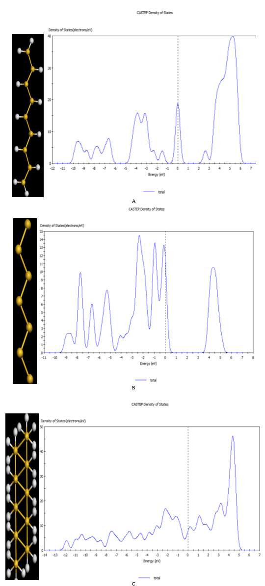
 | Figure 2. variation of total energies, bond length, and bond angle of monoatomic Si nanowire as a function of its length per atom |
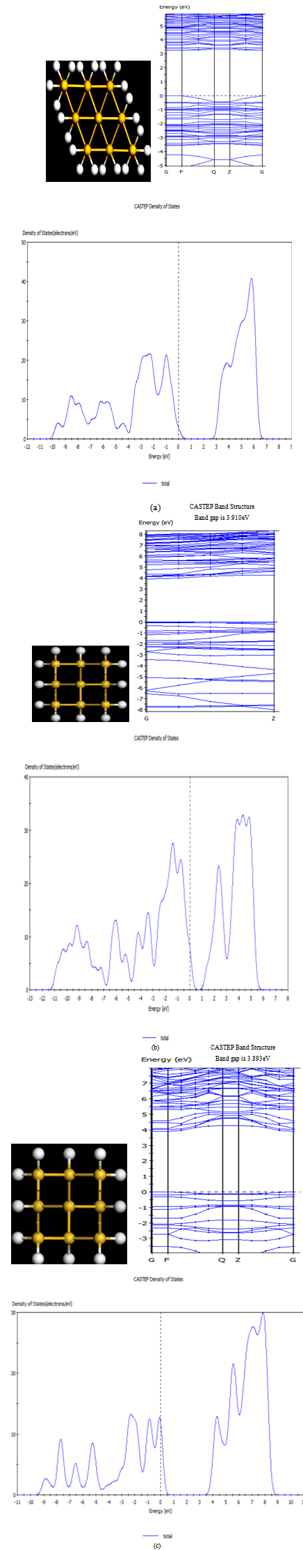 | Figure 3. Top view of (a) (111) Si nanowire, (b) (110) silicon nanowire and (c)[100] Si nanowire with their density of states |
4. Conclusions
- Present study reveals that Si nanowire, shows two energy minima as a function of wire length, like Au and Al[11] but quite different from another transition metal Cu and simple metals K and Ca. The stability of a structure is explained by its electronic structure. The 3p bands in Si nanowire play important role in its stability. The effects of generalized geometry approximation and local density approximation on cohesive energy and bond length of Si nanostructures are also analyzed and it is observed that that the cohesive energies obtained from generalized geometry approximation are more closer to experimental value than the cohesive energies obtained from LDA, which shows that the density functional is improved form local density approximation to generalized geometry approximation in Si.. The link from low dimensional 1D structure to high dimensional 3D bulk Si is estimated and the dimensional effect is discussed.
References
| [1] | H.Hofmann, Nanomaterials, Powder Technology LaboratoryVersion 1 Sept 2009 |
| [2] | Jaya Sarkar, Gobinda Gopal Khan† and A Basumallick, Bull. Mater. Sci., Vol. 30, No. 3, June 2007, pp. 271–290. |
| [3] | Erik C. Garnett, Mark L. Brongersma, Yi Cui, and Michael D. McGehee Annual . Rev. Mater. Res. 2011. 41:269–95 |
| [4] | B. Lassen, M. Willatzen, R. Melnik, L.C. Lew Yan Voon, J. Mater. Res., Vol. 21, No. 11, Nov 2006 |
| [5] | D. Sánchez-Portal, E. Artacho, J. Junquera, P. Ordejón, A. García, and J. M. Soler, Phys. Rev. Lett. 83, 3884 (1999). |
| [6] | H. Ohnishi, Y. Kondo, and K. Takayanagi, Nature (London) 395, 780 (1998). |
| [7] | A. Rubio, Y. Miyamoto, X. Blasé, M. L. Cohen, and S. G. Louie, Phys. Rev. B. 53, 4023 (1996) |
| [8] | L. Pauling, The Nature of the Chemical Bond (Cornell University Press, Ithaca, 1948), Chap. XI. |
| [9] | M. C. Payne, et al., Rev. Mod. Phys. 64, 1045 (1992). |
| [10] | V. Milman, et al., Int. J. Quant. Chem. 77, 895(2000) |
| [11] | M. C. Payne, M. P. Teter, D. C. Allen, T. A. Arias, and J. D. Joannopoulos, Rev. Mod. Phys. 64, 1045 (1992). |
| [12] | G. Kresse and J. Hafner Numerical computations have been carried out using VASP software., Phys. Rev. B 47, R558 (1993); G. Kresse and J. Furthmuller, ibid. 54, 11169 (1996). |
| [13] | W. Kohn and L. J. Sham, Phys. Rev. 140, A1133 (1965); P. Hohenberg and W. Kohn, Phys. Rev. 136, B864 (1964). |
| [14] | D. Vanderbilt, Phys. Rev. B 41, R7892 (1990). |
| [15] | Jin-Cheng Zheng, Hui-Qiong Wang, A. T. S. Wee and C. H. A. Huan, International Journal of Nanoscience 1(2): 159-169 (2002). |
| [16] | N. Y. Skorodumova, S. I. Simak, Computational Materials Science 17, 178-181 (2000) |
| [17] | K.P. Bohnen and K.M. Ho, Surf. Sci. Rep. 19, 99-120 (1993). |
| [18] | D. Sánchez-Portal, E. Artacho, J. Junquera, P. Ordejón, A. García, and J. M. Soler, Phys. Rev. Lett. 83, 3884 (1999). |
| [19] | D. Sánchez-Portal, C. Untiedt, J. M. Soler, J. J. Sáenz, and N. Agraït, Phys. Rev. Lett. 79, 4198 (1997). |
| [20] | M. A. Hopcroft, W. D. Nix, and T. W. Kenny, "What is the Young's Modulus of Silicon?", IEEE Journal of Microelectromechanical Systems, vol. 19, Issue 2, pp. 229-238, 2010. |
| [21] | Silicon Self-Diffusion in Isotope Heterostructures H.Bracht, E.E.Haller, R.Clark-Phelps: Physical Review Letters, 1998, 81[2], 393-6 |