-
Paper Information
- Next Paper
- Previous Paper
- Paper Submission
-
Journal Information
- About This Journal
- Editorial Board
- Current Issue
- Archive
- Author Guidelines
- Contact Us
International Journal of Optics and Applications
p-ISSN: 2168-5053 e-ISSN: 2168-5061
2014; 4(4A): 6-11
doi:10.5923/s.optics.201401.02
Three-Dimensional Point-Focus Spectral Splitting Solar Concentrator System
 Abstract
 Reference
 Full-Text PDF
 Full-text HTML
Carlo Maragliano1, Ahmed Zayan2, Marco Stefancich1
1Laboratory for Energy and Nano Sciences, Masdar Institute of Science and Technology, Abu Dhabi, UAE
2The Renewable Energy and Applied Photonics Laboratories, Electrical and Computer Engineering, Tufts University, Medford, Massachusetts, USA
Correspondence to: Carlo Maragliano, Laboratory for Energy and Nano Sciences, Masdar Institute of Science and Technology, Abu Dhabi, UAE.
| Email: |  |
Copyright © 2014 Scientific & Academic Publishing. All Rights Reserved.
Spectral splitting solar systems are emerging as alternative solutions to multi-junction solar cells for cost effective high efficiency photovoltaic applications. We have recently proposed a low cost single element splitting system based on a prismatic structure able to contemporary split the solar light into its spectral component and concentrate them. Here a new design of the spectral splitter is proposed and the optimization study of the entire solar system (solar splitter and solar cells) is conducted. The considered spectral splitter/concentrator consists of a three-dimensional point-focus system made of a disposition of dispersive elements. The advantages of this new design are discussed in detail and results of the optical simulations are reported. The optical system is then combined with a set of three solar cells, each of them illuminated with a different spectrum band. Simulations with Sentaurus TCAD are carried out with the aim of optimizing the electrical and geometrical properties of the devices. We obtained an overall efficiency of 28 %, which represents a good starting point for spectral splitting solar systems to compete with multi-junction solar cells technology.
Keywords: Spectral Splitting Solar Systems, Concentrated Photovoltaic Systems, Optical Simulations, Photovoltaic Cells, Homo-Junctions
Cite this paper: Carlo Maragliano, Ahmed Zayan, Marco Stefancich, Three-Dimensional Point-Focus Spectral Splitting Solar Concentrator System, International Journal of Optics and Applications, Vol. 4 No. 4A, 2014, pp. 6-11. doi: 10.5923/s.optics.201401.02.
Article Outline
1. Introduction
- In the last fifty years, the need for alternative and renewable sources of energy has become pressing. This is driven by environmental concerns, increasing demand for energy as well as by the progress in energy technologies. Among all renewable sources of energy, solar energy is by far the most abundant. This aspect, combined with its inexhaustibility, contributes to make this source very intriguing for energy harvesting.Photovoltaic (PV) technology is among the best ways to harvest this enormous amount of energy. Until now, different PV technologies have been proposed [1] and their capabilities in converting the solar energy into electrical energy have been reported [2]. However, in order to promote PV technologies to plant scale power generation level, some key issues need to be addressed [3, 4]. Addressing issues such as scarcity of raw materials, refinement cost and low efficiencies would allow reaching the grid-parity and making the PV technology costly competitive with other energy harvesting technologies.So far, different solutions to overcome the limitations of PV technology have been proposed. For single junction devices, attempts to reduce materials costs [5-7] and to increase energy absorption [8-10] have been proposed. However, due to the spectral width of the solar emitted radiation, the efficiency of any single bandgap solid state converter is inherently limited. These limitations have been object of intensive studies by Shockley and Queisser [11] who derived the maximum theoretical efficiencies of single-junction PV devices depending on their bandgap. The simultaneous use of a set of junctions made of different materials to convert the solar light provides a mean to overwhelm these limitations and to achieve higher efficiencies with theoretical limits approaching 85 %. This technological solution can be implemented stacking solar cells one on top of each other in the so called Multi-Junction (MJ) solar cells. The bandgap decreases from the uppermost to the lowermost cell and this allow the radiation that is not converted by the top cell to reach the lower one due to the material’s transparency to radiation below its bandgap. However, MJ solar cells impose severe restrictions in terms of material choice and growth processes. Lattice matching problems and consequent defects formation seriously undermine MJ solar cells performances. In order to minimize this problem, the fabrication process of such cells requires epitaxial growth techniques. This approach has been proved to be commercially viable in terrestrial systems only under very high concentration to offset the high cell cost. An alternative technological solution consists in splitting the light into spatially separated spectral region to be converted with properly selected single-junction solar cells. Proposed for the first time by Borden at al. [12], the main advantage of this approach is the accessibility to a broader group of materials. Indeed, lattice-matching requirement no longer applies since different junctions are not stacked one on top of the other, but are simply disposed in parallel. The validity of this approach is testified by several reports of high laboratory efficiencies, an extensive review of which can be found in [13]. We have recently proposed a two-dimensional single optical element system which integrates the concentrating and spectral splitting actions [14]. The optical element is defined as a set of solid transparent dispersive prisms, each operating independently. They are designed in order to deflect and split a polychromatic collimated light beam from a given direction onto the same area of a receiving target. The resulting concentrated and spectrally divided beam is simply obtained by the superimposition of each prism contribution. The orientation of the set of prisms is such that the light rays of a specific reference wavelength are mapped on the same target as depicted in Fig. 1.
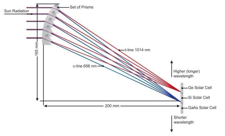 | Figure 1. Conceptual drawing of the concentrator/spectral splitting system proposed in [14]. The system is a set of microprisms designed to deflect two reference wavelengths on two distinct points on the photovoltaic receiver |
2. Optical Design Principles
- The optical element is made of a set of transparent dispersive prisms, each of them operating independently. They are designed to deflect and split a polychromatic collimated light beam onto a receiving target. Each of them contributes individually to the formation of the concentrated and spectrally divided beam. A dispersive prism is an optical element able to split a collimated beam of light according to the wavelength. This is basically due to the dependence of the phase velocity of the optical wave on its frequency. The essential parameters that affect the prism behavior are the angle formed by the entrance facet with the light rays (defined in Fig. 2 as I1) and the apical angle of the prims (defined as A).
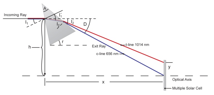 | Figure 2. Drawing of a single prism: A is the prism apex angle, I1 and I2 are the beam entrance/exit angle with respect to the relevant facets, r characterizes the rotation of the prism basis with respect to the optical axes, while h is the “height” of the entering light beam with respect to the reference center of the focal plane |
 | (1) |
 | (2) |
 , is defined via geometry by using Snell’s law such that every corresponding wavelength forms a point on a planar receiver that is no larger than 10 mm in width and height – typical dimensions for photovoltaic devices in a concentrated photovoltaic (CPV) system.Fig. 3 shows a schematic representation of
  in one prism constituting the 3D optical element. The value of the tilt angle varies along the dimensions of the concentrator in both transverse directions with respect to the incident light.
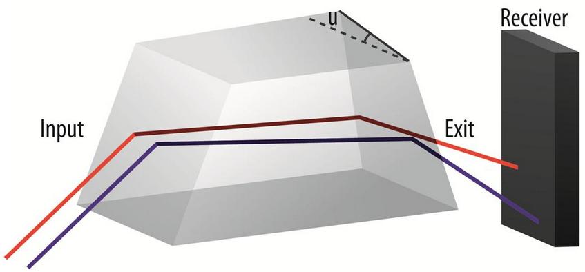 | Figure 3. Schematic illustration of one prism in the point-focus optical element. Note the angle  corresponding to the tilt the exit facet has with the entrance facet corresponding to the tilt the exit facet has with the entrance facet |
 , while maintaining a minimum average weighted optical transmission efficiency of 76%. The uppermost value for the concentration ratio is determined by the number of prisms in the optical element.
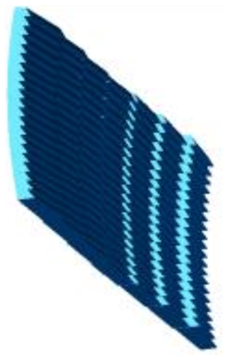 | Figure 4. Pilot 3D point-focus solar spectral splitting optical element |
3. Spectral Splitting Solar System
- The spectral splitting solar system we propose consists of the optical element previously introduced and a set of solar cells aimed at converting the spectrally separated solar rays.First of all, we designed the optical element in order to allow for the separation of the solar spectrum into
 bands, in which
  corresponds with the number of solar cells. For this study, we have chosen
  to be equal to 3, where each solar cell is obviously made of different materials (in the specific case GaAs, Si and Ge). The spectral content of each band has to be optimized in relation to the quantum efficiency (QE) of each photovoltaic device. In order to minimize the energy losses due to ‘hot carriers’ thermalization, the spectral content of each band is determined by considering as a limit the energy corresponding at each bandgap. By doing so, considering the well-known relation between the energy and the wavelength, we managed to divide the solar spectrum into 3 regions: below 780 nm to be absorbed with a GaAs solar cell, from 780 to 1100 nm to be absorbed with a Si solar cell and above 1100 nm to be absorbed with a Ge solar cell. For each band region, the total intensity as well as the spatial distribution of rays is simulated. The results of optical simulations conducted with TracePro are reported in Fig. 5.
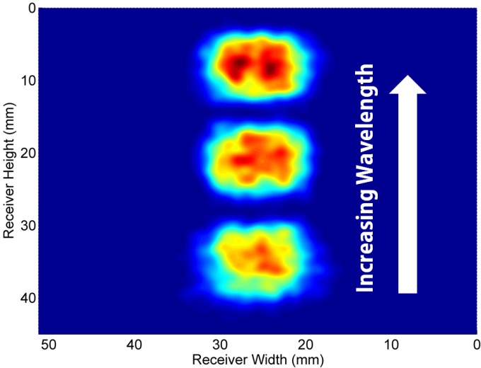 | Figure 5. Simulated flux map of three discrete wavelength regions |
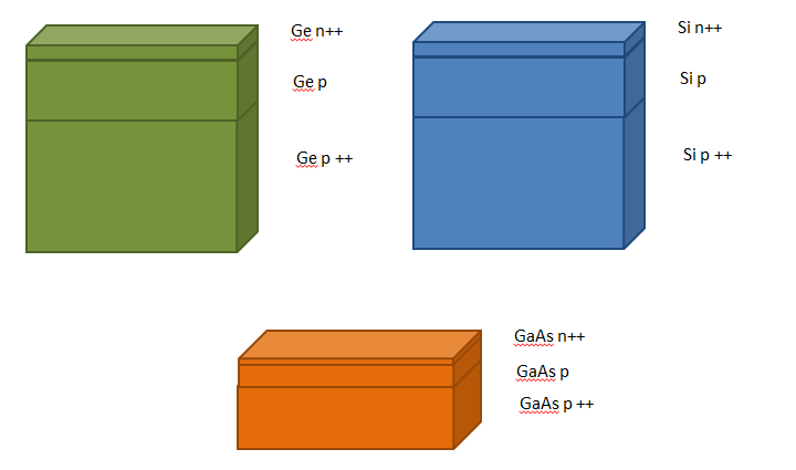 | Figure 6. Schematic of the three simulated solar cells (from the top left Ge, Si and GaAs). For all of them, the simulated structure is the following: n++/p/p++ |
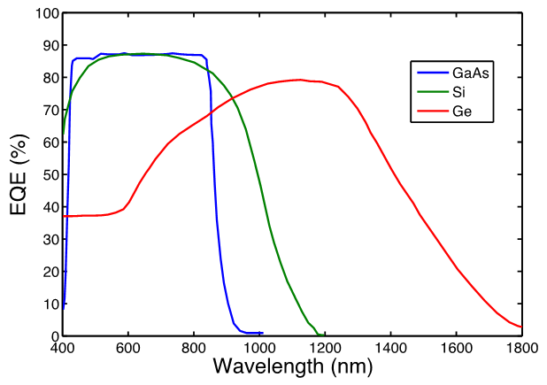 | Figure 7. Quantum Efficiency of the three simulated solar cells (GaAs in blue, Si in green and Ge in red) |
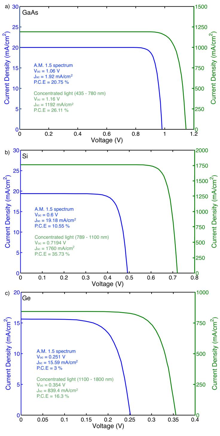 | Figure 8. Current density J versus voltage V curves of the three simulated photovoltaic devices [a) GaAs b) Si c) Ge]. For all of them, illuminated curves under full spectrum (blue curve) and concentrated/separated light (green curve) are reported |
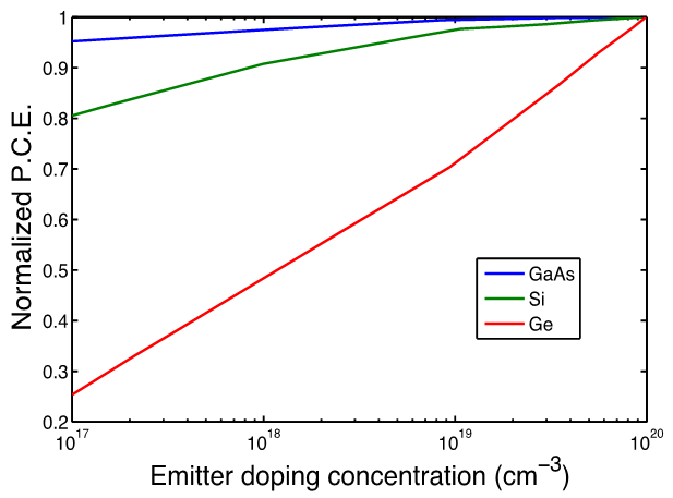 | Figure 9. Normalized efficiency versus emitter doping concentration for the three simulated devices (GaAs in blue, Si in green, Ge in red) |
4. Conclusions
- In this paper, we attempted a generalization and theoretical analysis of a promising approach for single component spectral splitting and concentration of sunlight. An evolution of the design of the previously proposed two-dimensional spectral splitting solar concentrator is presented. In order to design a three-dimensional system, a new degree of freedom (u) is introduced. This resulted in a point-focus system able to concentrate the solar spectrum with an average concentration of 90 suns across the 425nm – 1600nm range with a weighted transmission efficiency of 76%. The proposed photovoltaic system of cells comprised for GaAs for the high-energy region (425nm – 780nm), Ge for the low energy region (1100nm – 1600nm) and Si for the mid energy region (780nm – 1100nm) has been found to perform significantly better under the simultaneously concentrated and split light. Overall system efficiency was found to be in the order of 28%, making spectral splitting technology competing with current MJ solar cells.