-
Paper Information
- Previous Paper
- Paper Submission
-
Journal Information
- About This Journal
- Editorial Board
- Current Issue
- Archive
- Author Guidelines
- Contact Us
Microelectronics and Solid State Electronics
p-ISSN: 2324-643X e-ISSN: 2324-6456
2014; 3(1A): 30-35
doi:10.5923/s.msse.201401.04
Single-Event Transient Measurement on a DC/DC PWM Controller Using Pulsed X-ray Technique
 Abstract
 Reference
 Full-Text PDF
 Full-text HTML
Y. Ren1, L. Chen1, S.-T. Shi2, G. Guo2, R.-F. Feng3, S.-J. Wen4, R. Wong4, N. W. van Vonno5, B. L. Bhuva6
1Department of Electrical and Computer Engineering, University of Saskatchewan, Saskatoon, Canada
2Department of Nuclear Physics (DNP), China Institute of Atomic Energy (CIAE), Beijing, China
3Canadian Light Source (CLS), Saskatoon, Canada
4Cisco Systems Inc., San Jose, USA
5Intersil Inc., Milpitas, USA
6Electrical Engineering and Computer Science Department, Vanderbilt University, Nashville, USA
Correspondence to: L. Chen, Department of Electrical and Computer Engineering, University of Saskatchewan, Saskatoon, Canada.
| Email: |  |
Copyright © 2014 Scientific & Academic Publishing. All Rights Reserved.
Pulsed X-rays were used to perform Single-Event Transient (SET) measurements on a Commercial Off-The- Shelf (COTS) DC/DC PWM controller. The results were consistent with those of the previous heavy ion and pulsed laser testing, which indicates that the pulsed X-ray technique is a complementary tool to investigate SET. However, there are some limitations, such as low energy absorption of X-rays in silicon and Total Ionizing Dose (TID) effects due to the X-ray irradiation, which need to be considered during X-ray applications.
Keywords: Pulsed X-ray Technique, Single-Event Transient (SET), Pulse-Width Modulator (PWM), DC/DC Converter, Pulsed Laser, Heavy Ion
Cite this paper: Y. Ren, L. Chen, S.-T. Shi, G. Guo, R.-F. Feng, S.-J. Wen, R. Wong, N. W. van Vonno, B. L. Bhuva, Single-Event Transient Measurement on a DC/DC PWM Controller Using Pulsed X-ray Technique, Microelectronics and Solid State Electronics , Vol. 3 No. 1A, 2014, pp. 30-35. doi: 10.5923/s.msse.201401.04.
Article Outline
1. Introduction
- Currently, multiple testing techniques have been developed to perform Single-Event Transient (SET) investigation on electronic devices, such as heavy ion and pulsed laser techniques [1-3]. However, they both have some limitations. Heavy ion irradiation cannot provide precise time and physical location information of the ion hit, while the spot size of the pulsed laser is limited by its wavelength. A previous study showed that a picosecond pulsed X-ray technique, which features metal penetration and sub-micrometer resolution, can induce SET in GaAs/GaN High Electron Mobility Transistors (HEMTs) [4]. This result suggests a potential application of pulsed X-rays in SET investigation in modern electronic devices. In addition, the pulsed X-ray technique has a potential to achieve much better spatial resolution (less than 50 nm) for generating a more precise sensitivity map for circuits. However, it is still not clear whether pulsed X-rays can induce SET pulses that are big enough to affect the system function in silicon based CMOS technology. In this paper, a Commercial Off-the-Shelf (COTS) DC/DC PWM controller based on 600 nm BiCMOS silicon technology was used to investigate the practical application of pulsed X-rays on SET measurement. This DC/DC PWM controller was previously studied using heavy ion and pulsed laser irradiations [5] and was found to have a low threshold Linear Energy Transfer (LET). In other words, it requires a very low linear energy for the particles to trigger an SET. This makes it an ideal case to perform this study. Comparisons were made between the pulsed X-ray testing results and those from the previous heavy ion and laser experiments.The DC/DC PWM controller is the key part of the DC/DC converter circuit based on the pulse-width modulation technique shown in Figure 1. The circuit contains a Pulse-Width Modulation (PWM) block, power switching transistors and passive components. The PWM block further contains a PWM controller, a bandgap reference circuit, a soft-start circuit, and an error amplifier. The PWM block generates the signal that controls the duty cycle (designated as D) of the power transistor (or percent of time that the power transistor is ON). The converter topology determines the relationship between the DC input and output voltages. For the commonly used buck converter, the relationship is described by [6]
 | (1) |
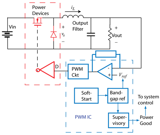 | Figure 1. Block level circuit diagram for a DC/DC converter [5] |
2. Experimental Details
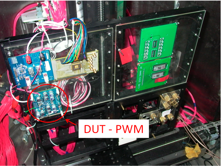
2.1. Device under Test (DUT)
- The DC/DC PWM controller under study is a triple regulator. It has two independent synchronously-rectified buck controllers and a linear controller to offer precise regulation of up to three voltage rails. The test circuit is shown in Figure 2. Each of the three soft-start pins is connected to a capacitive load. The PGOOD pin is an open-drain pull-down device. When power is first applied to the IC, the PGOOD output is pulled low indicating an initial condition. After all three soft-start pins complete their ramp up with no faults (no shorts detected on the switchers), the power is considered “GOOD” as indicated by a high PGOOD pin. The nominal output voltage for PGOOD is 5.7 V for this DC/DC PWM. Our previous testing [5] showed that a 6-μs SET pulse appeared on the PGOOD pin when the chip was irradiated with either heavy ions or pulsed laser beams. Our further analysis indicated that this is because the irradiation causes SET inside the PWM, which will cut off a NMOS current mirror on its propagation path when it is large enough. In this case, a 6-μs pulse is observed on PGOOD pin. On the other hand, if the SET inside the PWM is not large enough to cut off the NMOS current mirror, it will not propagate out and 6-μs pulse will not be observed on PGOOD pin. The 6-μs constant is the charging constant for a RC delay circuit connected to the current mirror. To sum up, a 6-μs pulse is only observed on PGOOD pin when the irradiation-induced SET inside the PWM is larger than a specific threshold. As a result, the PGOOD pin was used as an indicator in the pulsed X-ray experiment.
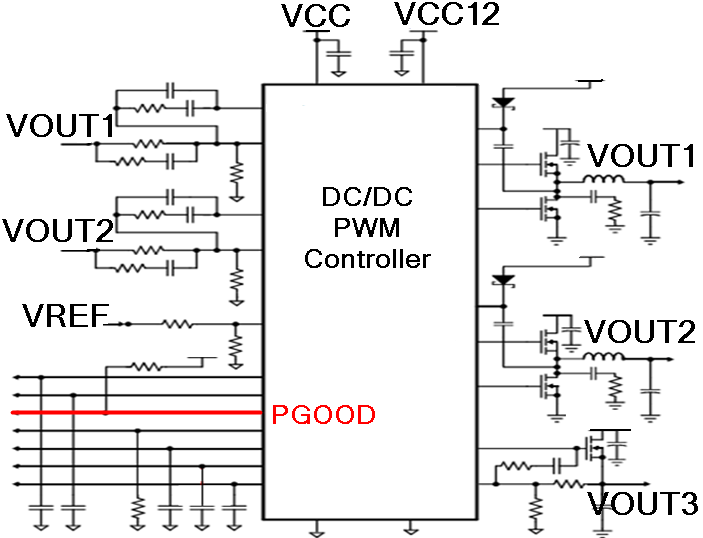 | Figure 2. Test circuit for the complete DC/DC PWM controller. [5] |
2.2. Irradiation Facilities
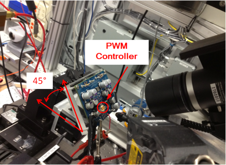
- The pulsed X-ray facility used for this study is the Very Sensitive Elemental and Structural Probe Employing Radiation from a Synchrotron (VESPERS) [7] beam line located at the Canadian Light Source (CLS, Saskatoon, SK, Canada). VESPERS has a hard X-ray microprobe capable of providing high level complementary structural and analytical information. The machine was operated at “single-bunch” mode to produce X-ray pulses with a pulse duration of ~540 ps and dark-gap of 570 ns (i.e., 1.75MHz). The energy of X-ray photons within the pulse ranges from 6 keV to 30 keV. Multi-bandpass and pink beam capabilities are built in to meet variable requirements. The spot size is around (2-4) μm by (2-4) μm. The sample setup for X-ray testing is shown in Figure 3. The test board was screwed to the acrylic sample holder which was placed at 45 degrees with respect to the X-ray beam vertically for better illumination and irradiation. Note that this incident angle can affect the X-ray spot profile and degrade its resolution.
 | Figure 3. The sample setup in the pulsed X-ray testing |
 | Figure 4. Experimental heavy ion testing setup in the vacuum chamber [5] |
3. Experimental Results
- In the X-ray experiment, a monochromatic X-ray pulse was applied to some sensitive nodes of the DUT (as determined by the laser scanning experiment [5]). The photon energy was varied from 7 keV to 20 keV. However, no SET (which is defined as a 6-μs or greater negative transient on the PGOOD pin) was observed on PGOOD pin of the DUT for these tests. For the next set of experiments, pink (polychromatic) X-ray pulses, which were composed of multiple bands and hence had much higher energy, were used to repeat the same experiments. 6-μs SET signatures were observed (Figure 5) on the PGOOD pin only when the X-ray pulse struck the most sensitive region of the circuit. This sensitivity of different regions was determined through laser testing [5]. These results showed that the nine bipolar transistors (used as a delta Vbe generator) inside a bandgap sub-circuit was the most sensitive region to single-event effects, as shown in Figure 6. Each one of the nine square blocks is a bipolar junction transistor. During this testing, the X-ray is not only applied to the active area, but also the different layers of metals. The 6-μs SET is observed all the time if only the X-ray is within the nine bipolar area. However, after 10 minutes of exposure, the X-ray beam failed to trigger any SET event even with maximum pink X-ray energy. As the experiment went on, it was also observed that the PGOOD output high voltage increased gradually from 5.7 V to 7.4 V. Later on, the PGOOD signal oscillated when X-rays were applied (Figure 7). To be more specific, the PGOOD signature started to oscillate when the X-ray pulse was applied. The time durations of the negative glitches were in the order of several seconds. In addition, after the X-ray irradiation was stopped, the PGOOD went through an oscillation process for about 20 minutes before it was finally stabilized at 7.4V. The time duration of the glitches decreased gradually along with this oscillation until they reached several hundred milliseconds. This complex phenomenon was not observed for previous heavy ion and laser experiments. This time-dependent phenomenon is a direct result of total dose effects as discussed below.
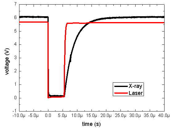 | Figure 5. SET induced at PGOOD output by X-ray and laser |
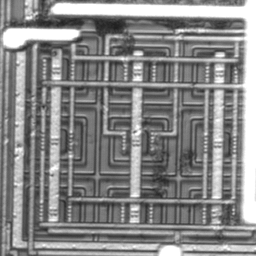 | Figure 6. Sensitive area in the pulsed X-ray testing |
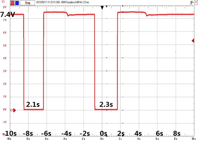 | Figure 7. Irregular oscillation at PGOOD pin |
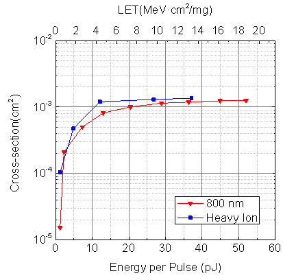 | Figure 8. The heavy ion and laser experiment results |
4. Discussions
- From the X-ray experiment results, it is observed that the pulsed X-rays generally have the same ability as the pulsed laser and heavy ion in terms of inducing SET in the DC/DC PWM controller fabricated in 600 nm BiCMOS technology. It is obvious from our experiment that pulsed X-ray technique has its own advantages over both pulsed laser technique and heavy ions in terms of SET evaluation. For example, when the pulsed laser is applied to the metal layers of the die, no SET will be ever observed because the pulsed laser will be blocked by the metal. It is a different situation for pulsed X-ray who has the capability to penetrate the metal. This advantage is supported by our testing when the pulsed laser is applied to metal layers and the SET appears. The pulsed X-ray is much more convenient in locating the sensitive devices compared with its heavy ion counterpart. Our experiment clearly showed that the nine bipolar is most sensitive while it will be harder for heavy ion testing to get this information. However, there are some aspects that need further study. First, the X-ray charge deposition level in the sensitive volume is different from that observed for heavy ion and pulsed laser testings. The X-ray photon has higher energy than the pulsed laser photon. However, its absorption is much lower. The X-ray absorption mainly depends on the target material, the sensitive volume thickness and the X-ray energy. For example, the energy absorption of a 30 keV X-ray photon in 1 μm silicon is around 0.027% [9]. This low absorption coefficient reduces the charge deposition in the sensitive volume of the chip. As a result, it is difficult to generate an effective chip-level SET unless the required critical charge at the specific node is small. In our testing, monochromatic X-rays failed to cause SET in the PWM chip. Our pulsed laser experiments showed that the PGOOD SET threshold laser energy for this DC/DC PWM controller is 1.2 pJ for 800 nm laser wavelength, and heavy ion experiments showed a threshold LET of less than 0.4 MeV-cm2/mg. The results imply that samples have to have low threshold LET in order to be suitable for pulsed X-ray study. These results also imply that the pulsed X-ray diagnostic technique is applicable only to low SET threshold commercial devices and is at least for the present of limited utility for investigating formally SET hardened part types. Further experiments are required to correlate the X-ray energy in silicon technologies to other experimental results using pulsed laser and HI irradiation. We are correlating the energy using a diode fabricated in the IBM 130 nm CMOS technology.Second, Total Ionizing Dose (TID) affects the validity of the SET test results. TID is a potential limitation to SET investigation using the pulsed X-ray technique. In our testing, the laser instead of X-ray fluorescence was used to image the chip, which diminished the X-ray irradiation. However, TID effects were observed during the testing, with the maximum PGOOD SET voltage level increasing for successive tests, especially when the pink X-ray beam was used. This maximum voltage level increase was found to be non-recoverable even when a power cycle is applied or the DUT was powered off for five days. TID also changed the X-ray pulse threshold energy of the DUT. As a result, even the pink (higher energy) X-ray pulse was unable to induce a 6-μs SET after the X-ray irradiation. This is believed to be due to gain degradation of the bipolar transistor devices in the bandgap sub-circuit caused by the X-ray irradiation. The TID effect is more serious in complex analog/mixed signal system as the changes in device parameters along with the complex circuit architecture tend to cause unexpected system responses such as the oscillation we observed in our case.
5. Conclusions
- This paper compares SET testing results using the pulsed X-ray technique with earlier results using the heavy ion and the pulsed laser. The advantages and limitations of the pulsed X-rays as a practical method for SET investigation were presented and analysed. The results show that the pulsed X-ray technique is a potential tool to study SET, especially for devices with low threshold LET. It has its own advantages over both pulsed laser technique and heavy ions evaluation method. It is easier to located the sensitive devices with pulsed X-ray than heavy ions evaluation. Also, it is more accurate than pulsed laser technique in terms of pinpoint the sensitive area due to its capability to penetrate metal layers. For example, the laser cannot detect the sensitive area if it is underneath metal layers while pulsed X-ray can. However, its low effective LET and the effects of TID may present potential problems for general applications. Also, future work including testing of a diode structure will be done to correlate pulsed X-ray results with those obtained earlier for pulsed laser simulation in silicon technology. The diode has the advantage of simple structure over the DC/DC PWM controller in SET investigations. In other words, the diode can show the initial width and amplitude of the SET while the DC/DC PWM controller is blocking the information due to the components on the SET propagation path. As a result, more insights on X-ray induced SET will be gained in our future study using the diodes.