-
Paper Information
- Next Paper
- Previous Paper
- Paper Submission
-
Journal Information
- About This Journal
- Editorial Board
- Current Issue
- Archive
- Author Guidelines
- Contact Us
Microelectronics and Solid State Electronics
p-ISSN: 2324-643X e-ISSN: 2324-6456
2014; 3(1A): 17-29
doi:10.5923/s.msse.201401.03
Analog Integrated Circuit Sizing and Layout Dependent Effects: A Review
 Abstract
 Reference
 Full-Text PDF
 Full-text HTML
Tuotian Liao, Lihong Zhang
Department of Electrical and Computer Engineering, Faculty of Engineering and Applied Science, Memorial University of Newfoundland, Canada
Correspondence to: Tuotian Liao, Department of Electrical and Computer Engineering, Faculty of Engineering and Applied Science, Memorial University of Newfoundland, Canada.
| Email: |  |
Copyright © 2014 Scientific & Academic Publishing. All Rights Reserved.
In order to generate a quality-guaranteed tape-out as the objective of CMOS design, diverse analog integrated circuit synthesis flows have been proposed to address the drawbacks of the traditional iterative design flow that may meet performance requirements but super time-consuming. Due to the indispensable impact of Layout Dependent Effects (LDEs) on electrical performance, standard models of LDEs have been developed to consider stress incurred effects such that simulation tools with built-in LDE models would provide results with higher accuracy at the advanced technology nodes. In addition to a survey of the universal synthesis flows, this paper put more emphasis on layout-aware circuit sizing by exhibiting a comprehensive literature review in this area. In particular, two dominant LDEs, Well Proximity Effects (WPE) and Shallow Trench Isolation (STI) effects, are discussed along with our experiments that aim to illustrate the severity of the induced performance degradation especially on sensitive devices even in the general analog integrated circuit building-blocks. Based on the exposed relationship between LDEs and circuit performance as per our experiments, the layout-related issues need to be seriously addressed in the next-generation analog synthesis methodologies and flows.
Keywords: Circuit Sizing, LDEs, WPE, STI
Cite this paper: Tuotian Liao, Lihong Zhang, Analog Integrated Circuit Sizing and Layout Dependent Effects: A Review, Microelectronics and Solid State Electronics , Vol. 3 No. 1A, 2014, pp. 17-29. doi: 10.5923/s.msse.201401.03.
Article Outline
1. Introduction
- Semiconductor industry aims at developing more compact electronic products while maintaining higher speed and increasing functionality at lower cost. Moore’s Law provides sound prediction to scalability of MOSFETs in industry that facilitates to achieve this objective. From the old technology to contemporary 20nm and below technology nodes, analog integrated circuit synthesis flow is never an obsolete topic as it is the key from the designers’ perspective to provide a stable, malfunction-free, and low-cost design regarding power, chip area and redesign effort, and further a successful type-out with sufficient design-for-manufacturability included. In the course of pursuing a high quality tape-out design, Layout Dependent Effects (LDEs), which are not prominent at old technology nodes, becomes increasingly influential with respect to circuit performance in the advanced technologies. Electrical parameter variations have been widely observed due to the stress incurred effects.A macro standpoint of analog circuit synthesis includes topology selection, device sizing and layout generation (i.e., placement, routing and parasitic extraction). In the micro scope at the circuit level, it only comprises topology formation and device sizing, whereas layout synthesis referring to the stage of layout generation resulting in a post-layout netlist is excluded from circuit synthesis. According to Kruiskamp and Leenaerts [1], circuit topology selection is to select device set out of hundreds of combinations. Each set behaves as one stage of the whole design at the schematic level. For instance, an operational amplifier (OPAMP) is composed of an input stage, a gain stage, and an optional output buffer. Das and Vemuri [2] introduced a genetic algorithm (GA) based framework for topology synthesis based on their previous work, ATLAS. Detailed classification of design automation techniques for topology synthesis before 2008 can be found in [3].With respect to circuit sizing, this design stage is targeted at determining device geometry that is necessary in early part of the design flow. Device geometry, specifically in CMOS technology, mainly refers to transistor width (W) and length (L), and resistor/capacitor/inductor nominal value. Some others may include circuit bias information into the sizing task. Till now, circuit sizing is still mostly done manually or semi-automatically by experienced analog designers and therefore is a time-consuming and error-prone task [4]. Automatic sizing tools are normally very application (i.e., circuitry) specific and problem (i.e., specification) specific.Layout generation following the completion of the sizing stage is a critical process, which can significantly affect the performance of fabricated chips. It is common that a well-designed circuit at the schematic level but omitting layout consideration is not able to function after fabrication in the advanced technologies. Layout information refers to physical placement and wiring with implication of parasitics and performance-related effects brought about by neighboring devices and common underneath substrate. Those effects are found to be extremely prominentand can cause performance degradation when a symmetric structure (e.g., current mirror and differential pair) appears in a mismatch manner. As the technology scalesdown towards even finer grid, LDEs become more significant. Traditional design flows handle LDEs in an iterative redesign manner until all the specifications are satisfied. Apparently, this costly redesign flavor is not beneficial. Therefore, some so-called layout-aware synthesis approaches have come into being. This paper will mainly conduct a comprehensive literature review on layout-aware synthesis approaches. Furthermore, some work on improving efficiency in terms of less design cycles is also discussed besides the introduction of parasitic modelling as well as Well Proximity Effects (WPE) and Shallow Trench Isolation (STI) modelling.The rest of this paper is organized as follows. Section 2 reviews most of the published works from the literature on analog layout-aware sizing up tolate 2013 to the best of our knowledge. In addition, the background of WPE and STI is introduced. Section 3 gives the standard modelling for WPE and STI used in most prevalent Electronic Design Automation (EDA) tools. Section 4 provides our experimental findings on WPE and STI affecting circuit performance. The last section concludes this paper in addition to providing recommendations and implications to analog designers.
2. Layout-Aware Circuit Sizing
- An overview of the state-of-the-art synthesis techniques appearing before 2008 has been documented in [3], where the classification criterion is based on the methods for attaining circuit architecture or topology as the first stage in the design & synthesis flow of analog integrated circuits. As our focus in this paper, circuit sizing, also known as design parameter optimization, normally takes place during or after the topology selection. The sizing objective, which is supposed to be closely related to performance, can be alternatively evaluated by analytic equations (sometimes called cost function), numerical simulation that can more closely reflect the real-world circuit performance, lookup table that is somehow a mapping to selective simulation results, symbolic analysis or performance models [3]. Different emphasis on various sizing properties can result in diverse optimization approaches. Therefore, in this literature review of layout-aware analog integrated circuit sizing, we categorize the covered works into a limited number of bins. Firstly, the main criterion of categorization is the technique for realizing the sizing task. Secondly, it is based on the degree of simulation involvement for performance evaluation. Lastly, the pattern of layout generation as well as parasitic estimation is another criterion. The details of categorization by using these three criteria are discussed below along with the review of each work.
2.1. Layout-Aware Sizing Techniques
- Based on the criterion of how to achieve the sizing objective, the layout-aware sizing works published in the past can be categorized to four groups: stochastic-based, deterministic-based, geometric-programming or symbolic-analysis-based, and Gm/Id-based techniques.
2.1.1. Stochastic-Based Techniques
- Circuit sizing is getting even popular at the advanced technology nodes. Since the 1990’s, besides the universal application to the other fields, gene inspired evolutionary algorithms have been applied to the circuit sizing domain. Even though the convergence for this type of stochastic-based algorithms (including genetic algorithms, simulated annealing, particle swarm optimization, and other) is hardly proved, optimal solutions can be empirically found via a smart guide during the exploration process. Some control parameters, e.g., mutation and crossover rates in genetic algorithm, determine the searching quality by balancing the weight between overall exploration and localrefinement.Many works in the last decade of the 20th century dealt with topology selection and sizing separately, thus overhead was inevitable when useless topology was generated. Authors in [1] claimed their CMOS OPAMP synthesis tool called DARWIN, using genetic algorithm, can simultaneously deal with topology selection and sizing. They translate circuit specification and constraints into certain representations used in genetic algorithm in order to require less expert knowledge for circuit optimization. Their tool can cover different topologies in an efficient way. However nowadays, as the CMOS technology is scaling down, this tool may not be applicable due to lack in addressing many LDE issues (e.g., WPE and STI), which were not found prominent at the old times.Vancorenland et al. [5] promoted the idea of analog circuit design from [1] to a new one involving tasks of circuit sizing and layout generation, in addition to parasitic estimation mainly addressed in [6]. The coupling of sizing and layout generation was made possible in the proposed layout-aware synthesis method, which contained differential evolution algorithm optimization, equation application (cost function), numerical simulation, and layout generation by using layout templates. The adopted Hooke algorithm in fitting the cost function was non-stochastic and thus contributed to faster convergence. The evaluation of the fitted cost function employed a mechanism that combined few steps of model approximation with one simulation insertion to refine the model. According to the authors, this combined evaluation mechanism could largely increase the accuracy. However, this improvement was ensured at the cost of actual layout generation and detailed parasitic extraction.According to Rutenbar [7], Simulated Annealing (SA), which is a statistical and heuristic process, uses either some numerical cost functions or circuit-level simulation for verification. Design knowledge based optimization is usually integrated with such a heuristic technique to improve exploration efficiency. For instance, De Ranter et al. [8] presented a specification-driven layout-aware CMOS RF design tool called CYCLONE. They used Adaptive Simulated Annealing (ASA) package as their search engine. A thought similar to [5] is that the circuit sizing and layout generation are combined for the optimization of oscillators. This tool includes three major components, the optimization startup, the optimization loop using electromagnetic simulation, and the layout generation. The design configuration file and technology layout file are inputs of the layout tool to form leaf cell branches, which are used as the building blocks to the final layout. The use of parameterized leaf-cell-based design method facilitates parasitic estimation in each layout generation step. The use of technology-independent template-based layout generation decreases the effort to generate redundant physical layout as that in [5].Agarwal et al. [9] illustrated the importance of including layout information in circuit sizing by comparing the deviation in performance with and without parasitic consideration. Their core engine to size the circuit is SA. Ranjan et al. [10] proposed a slightly different approach, which uses a symbolic performance models (SPM) generated by using equations from small-signal models. The SPM is used as the evaluation method instead of real simulation in the sizing engine of SA. Due to the integration of intelligence into performance evaluation (by using symboliccost function), it can also be grouped into the symbolic-analysis-based techniques detailed in Section 2.1.3.Another work from Agarwal and Vemuri [11] used a similar sizing engine, but put more emphasis on the estimation of layout parasitics in RF circuit synthesis considering worst-case corners.Choi and Allstot [12] employedparticle swarm optimization (PSO) and ASA for parasitic-aware RF circuit design. The proposed design process used a commercial simulator, such as HPSICE or SPECTRE, along with curve fitting tool in MATLAB to provide parasitic-aware synthesis. However, the details of parasitic modelling are unclear from the paper. Although the design process looks to be faster than the conventional SA technique, the two provided examples show the number of iteration to be more than 1000. From common sense, applying curve fitting for parasitic modelling and using a commercial simulator with a large number of iterations are likely to be expensive in terms of CPU time.An integrated circuit sizing method with floorplan variation plus simulation for performance evaluation was introduced in [13]. At each step a floorplan is generated and parasitics are estimated using the floorplan and transistor size. After convergence, several floorplans are considered for performance evaluation. Once a floorplan is selected, a layout is then generated, extracted and verified. If the specification is not met, the loop would be executed again. This simulation based method tends to be CPU-time costly. Although the core of sizing in this paper is not reported in further detail, its iterativetrail-and-see mechanism moves us to consider this work inside the category of the stochastic-based techniques.
2.1.2. Deterministic-Based Techniques
- Any gradient-based error-minimization-directed optimization technique falls into this category. The normal way is to propose an objective function mostly featuring minimization of an error resulting from the difference between specification and evaluation.Schwencker et al. [14] proposed an automatic sizing method for analog integrated circuit. They introduced structural constraints as circuit knowledge in the sizing process. Their sizing algorithm is based on linearization with sensitivity coefficient and gradient-based method for better convergence. The authors claimed that considering structural constraints could reduce design parameters and cut down simulation time, as well as being insensitive to process variation.Dessouky et al. [6] introduced an approach incorporating layout parasitics and physical layout constraints during the sizing process in early design stage. This approach shortens the sizing-layout iteration by using the following two knowledge-based tools. Their sizing tool runs first when every device folds. During the parasitic calculation process, the sizing tool continues to run and interact with a constraint-driven layout tool iteratively to make compensation for parasitics up to the point where parasitics keep unchanged. After this, a real layout is generated. That is to say, physical layout generation is just one-time cost. Their sizing engine (COMDIAC) is a semi-deterministic tool. The heuristic trial for dc current needed for every transistor to realize the given specification is considered to be a stochastic approach, whereas for a given trail current, the transistor sizes can be calculated via simple monotonic numerical calculation and thus considered to be deterministic.Habal and Graeb [15] proposed an automatic layout-driven synthesis flow. Their sizing steps include partitioning the problem into sub-problem by using linearized approximation of constraints and specification with respect to design parameters in a manner identical to [16], and then solving sub-problem by using a modified trust-region algorithm. The whole work even includes SPICE simulation for evaluation, parasitic capacitance extraction by an integral equation field solver, and placement optimization with B*-tree. In some optimization approaches, the designers’ knowledge is imperative to continue the sizing process, which is based on a deterministic algorithm introduced in [17]. The entire synthesis process was arranged at the cost of additional effort in layout exploration and extraction. Overall this work is quite comprehensive in the circuit synthesis domain, although it tends to experience costly layout generation for every sized alternative. Another deterministic algorithm in [18] was proposed to consider process variation in the automated design of analog circuits that include mismatch-sensitive components. With respect to the consideration of manufacturing and operating variation, Schwencker et al. [17] proposed a generalized boundary curve (GBC) to decide the step length within an iterative trust-region optimization algorithm. Applying the nonlinear cost function on the linearized objectives can largely cut down the iteration number during the optimization.A sizing approach by using combined techniques was proposed in [19]. In this work, a transistor-level simulator (HSPICE) is used with simulated annealing technique for the first phase of sizing. In the second phase a deterministic method is used. Template-based layout generation, which takes a few seconds to generate layout, is deployed along with Cadence PCELL and SKILL programming language [20]. At first the sizing engine selects a set of random values within a range. For those values, the Geometric Constraint Module selects a candidate from a set of layout styles. And then the parasitics are extracted from the selected layout and the performance is evaluated. If the specification is not met, the loop is executed again.
2.1.3. Geometric-Programming-Based or Symbolic-Analysis-Based Techniques
- In this category, local unconstrained optimization is adapted to constrained optimization, such as Geometric Programming (GP), which keeps popular for fast analog synthesis. It is a convex optimization problem, which can include a set of performance constraints modeled from the given technology parameters and the required specification, as well as a set of symbolic interconnect parasitics formulated with geometric requirements and floor planning. The symbolic floor planning and routing constraints enable to use a set of parasitic expressions so that interconnect parasitics can be enclosed inside the circuit sizing phase. Finally, a GP solver [21] is deployed to provide a solution, which not only attains the desired circuit performance but also concurrently considers layout induced parasitic effects. Such GP solvers, using standard interior point algorithm [21] and being able to solve large convex optimization problems efficiently, can be readily accessed in the public domain.Reference [22] exhibited a fast parasitic-aware synthesis approach, which considers the performance constraints and layout induced parasitics simultaneously within a concurrent phase of circuit synthesis. The GP-based sizing algorithm can include both device intrinsic parasitics and interconnect parasitics induced from layout floor plan. The analytic expressions of interconnect parasitic substrate and coupling capacitance can be further improved with the aid of the workin [23]. Another single-GP-process-based optimization [24] divides the design space into sub-problem by using piecewise-linear fitting (PWL) instead of genetic-algorithm- based modelling (GAP) in order to achieve accuracy improvement without compromising complexity. Given specific performance requirement and circuit topology, only a limited number of sub-spaces is needed and calculated rather than a costly blind search for all the sub-spaces. Without involving multiple GP execution for fine tuning, the optimization efficiency can be improved. However, a sound balance ought to be made between the GP process execution iteration and the knowledge-involved design effort regarding sub-space simplification.
2.1.4. Gm/Id-Based Techniques
- Based on the fact [25] that transconductance over drain current (gm/Id) is only related to node voltage (Vgs) regardless of device size, a Gm/Id-based approach is applied in the analog circuit sizing domain. A pre-built table from unit-device numerical simulation results is maintained for a given technology node. This table reflects the mapping information among reference current (IREF), reference size (SREF) under a given bias condition, and constant node voltages (Vg, Vs, and Vd).Driven by a similar idea of layout-aware synthesis, Liao et al. [26] developed a user-friendly GUI in a layout-aware analog synthesis tool (LASER). Anovel parasitic-aware circuit sizing flow was provided to realize the combination of sizing and layout consideration. This work is similar to [27], both of which are based on a bias-driven sizing approach introduced in [25].Tracing back a little further, these three works should be credited to [28], which promoted the Gm/Idmethodology originated from[29]. Although the bias-driven sizing approach seems to be able to reduce the modelling effort and improve the modelling accuracy, these works suffer from a lack of sufficient details on Gm/Id lookuptable maintenance as well as parasitic modelling. In addition, reference [25] fails to provide any modelling equations for intrinsic capacitance over current (C/Id), which seems ideally linear from the provided chart. In addition, according to its methods on how to resolve optimal node voltages and conduct Gm/Id by linear programing, we can also categorize it into the symbolic-analysis-based techniques detailed in Section 2.1.3.In summary, the convergence of the stochastic-based techniques is hard to be proved mathematically and the execution time is mostly undesirable, although they are often resorted to as a practical search engine for optimal solutions. The deterministic-based techniques meet the industrial preference of generating fixed output results given one input. However, how to escape local minimais always a challenging task for the construction of sound deterministic algorithms. If a thorough traversal scheme is deployed, the required analog designers’ domain knowledge, which is indispensable to reduce the optimization complexity, is always found to be over the head of regular users. In contrast, the guaranteed optimality and short execution time are highly favorable for the GP-based or symbolic-analysis-based techniques. However, there is controversy regarding GP modelling accuracy for analog integrated circuits. Nevertheless, the GP-based or symbolic-analysis-based techniques can perform very well if they are used as the first stage followed by another stochastic or deterministic-based sizing stage. Gm/Id-based techniques have a problem on the construction and maintenance of lookup tables for different technologies. Their efficacy needs to be confirmed especially at the advanced technology nodes. Despite that, the idea of design target transformation from devicegeometry to bias condition is indeed insightful.
2.2. Other Categorization Criteria
- The previous works on the layout-aware analog sizing from the literature can be also categorized as per other criteria, that is, how to evaluate performance during the sizing process, or how to generate layout and estimate parasitics.
2.2.1. Schemes of Performance Evaluation
- The easiest and almost the most accurate way of performance evaluation is device-level numerical simulation, which is widely supported in prevalent EDA tools. Due to the high cost in CPU time, analytic equation (or cost function) based approach is an alternative to evaluate circuit performance. Considering the controversial accuracy of the analytic/cost-function modelling, a smart combination of both approaches above seems favorable regarding the balance between efficiency and accuracy. For simplicity and clarity, only the reference index is listed below according to the applied schemes of performance evaluation. As for the process of verification, numerical simulation is actually used in almost every work. So here the categorization is made on the performance evaluation at the sizing stage instead of the final verification stage.1. Numerical simulation: [9, 12, 13, 15, 16, 18, 19, 31];2. Analytic/cost-function: [1, 2, 8, 10, 11, 14, 17, 22, 24];3. Combination of numerical simulation and analytic/ cost-function: [5, 6, 25, 26, 27, 28, 29].As those Gm/Id-based approaches need lookup table construction with data coming from numerical simulation for a given technology, we group them into the combination class.
2.2.2. Schemes of Layout Generation and Parasitic Estimation
- Traditional layout generation is mostlya manualprocess and thus time-consuming and error-prone. Thanks to the accomplishment of PCELL-like tools, schematic-driven layout generation flow has been built in popular EDA tools, such as Cadence Virtuoso [20]. This can be somehow treated as a semi-automatic process because the actual placement relies on the knowledge of analog designers. Furthermore, multiple device properties need to be set one by one, like bulk style (integrated or detached), S/D orientation, dummy margin, intra-device pre-routing (gate routing),etc., which prolongs the design process. Routing tasks are accomplished through different algorithms, whose quality depends on net weight, symmetric constraints, and parasitic consideration.After that, parasitic estimation follows, which can be categorized in four groups: using commercial off-the-shelf extractors such as Mentor Graphics PEX [30], using macro models, using analytic estimation models along with curve-fitting parameters, and no parasitics considered or unclear in the estimation method.Reference [9] removes the actual layout generation and parasitic extraction from the optimization loop. Instead it presents a macro model for parasitic capacitance estimation. It divides the circuit into different modules and devises models for inter- and intra-module capacitance. It uses a procedural layout generator (PLG) environment called MSL (Module Specification Language) to generate parameterized layout after the completion of sizing and an off-the-shelf extractor is used to extract the layout parasitics. As the module size may change during the iteration, it creates a lookup table called Module Characterization Table (MCT). By using this MCT and linear interpolation, the work of [9] is able to estimate the parasitic values during circuit sizing phase. Data in the MCT is used to construct a variety of macro models. One prominent drawback for the interpolation operation is that the change in capacitance at smaller technology nodes, especially fringe capacitance, might not be linear to geometry size as overlap capacitance.Another aforementioned work [10] also used MSL to generate layout and off-the-shelf extractor to extract parasitics. Its key featureis that the adopted SPM can take all the capacitances in the small-signal model and combine some contributing parasitics identified from previous sample layouts. In [11], SA is first used to size the circuit by simulating the netlist with presence of parasitics, which is obtained from MCT discussed above. When converging, it finds a feasible region and determines the worst-case parasitics by using the feasible region with a placer. Then it makes local changes to cope with the interconnect capacitance for the worst-case scenario. In addition to corner analysis that is taken into account within this work, the methodology heavily suffers from high CPU-time cost of SA and off-the-shelf extractor. Besides that, making local changes might result in considerable capacitance variation compared to the parasitics previously estimated.Another parasitic-aware sizing method proposed in [31] is close to the traditional approaches. But instead of taking single layout information, it considers the parasitics of several previous runs to resize the circuit. In each loop, the circuit is resized, placed, routed, and extracted. An off-the-shelf extractor and simulator are used to extract parasitics and run simulation. At each step, the best- and worst-case capacitance corners are generated to make the optimization robust. However, one disadvantage of this work is inclusion of routing, floorplanning, and extraction inside each loop as well as performance evaluation with a commercial simulator might take a long time for the optimization to converge.The following is the detailed categorization for the review purpose:1. Off-the-shelf: [10, 15, 17];2. Marco-model: [9, 11, 31];3. Analytic estimation model: [5, 6, 8, 13, 19, 22, 23, 26, 27];4. No parasitic consideration or unclear: [1, 2, 12, 14, 16], 18, 24, 25, 28, 29].A summary of the adopted classifications on the previous works is illustrated in Table 1.
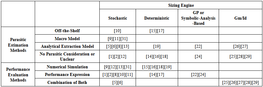 | Table 1. Summary of the adopted classifications for the previousworks |
3. Design Automation with Layout Dependent Effects
3.1. Well Proximity Effects (WPE)
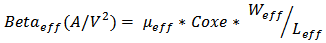
- The layout dependent effects discussed in this paper mainly include WPE and STI. They largely affect the performance of the circuit if not properly handled. During the implant process, some of the ions scattered from the edge of photoresist are implanted in the silicon surface near the mask edge, changing the threshold voltage of these devices by upwards of 100mV [32]. This effect is known as well proximity effect. The result of WPE is the formation of a graded channel due to a MOSFET placed too close to a well edge. This graded channel can cause the shift of electrical characteristics of the MOSFET.The WPE is a strong function of the distance of a MOSFET from mask edges. The electrical parameters of the MOSFET due to WPE show larger variation if it has shorter distance from the edge of well mask. As exposed in the BSIM model [33], they can be analytically expressed in the following,
 | (1) |
 | (2) |
 | (3) |
 | (4) |
 | (5) |
3.2. Shallow Trench Isolation (STI)
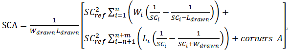
- The shallow trench is formed during the process of transistor isolation by etching onto the wafer and filling with silicon oxide as isolation between active areas. This exerts mechanical force, which is a compressive stress applying to the vicinities, i.e., diffusion areas. This stress is commonly referred as STI stress, also called Length of Diffusion (LOD) effect. SA/SB, STIW and other STI-related parameters are illustrated in Figure 1. SA/SB is a pair of distance parameters measured from the edges of each poly finger to its corresponding diffusion edges. For a layout netlist, each finger has its individual SA/SB pair. The width of STI (i.e., STIW) is measured from the edge of a device to its adjacent active area. A linear relationship between stress and layout information, SA and SB, is modelled by BSIM [33].
 | (6) |
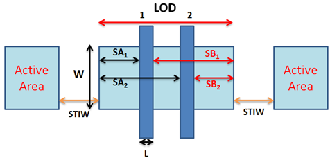 | Figure 1. Illustration of STI factors |
4. Verification and Experiment
4.1. Impact of WPE Mismatch
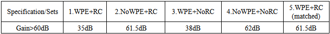
- The verification of WPE is straightforward as the WPE-related instance parameters SCA, SCB, and SCC are already considered in SPICE simulation with their presence in netlist. One can easily calculate SCA/SCB/SCC once layout information (i.e., transistor width, length, and well geometry) is obtained. By calculating SCA/SCB/SCC and comparing them with the ones used in extraction tool (such as Mentor Graphics Calibre [46]), one can verify whether those values match. These values can be edited in a netlist followed by re-simulation for any investigation purpose. Furthermore, to disable the calculation of SCA/SCB/SCC, one can easily disable WPE by setting WPEMOD = 0.In the following example, we will show a small mismatch of WPE in any match-sensitive structure would cause large variation of electric properties and even lead to circuit malfunction. Figure 2 shows a stack style of current mirror layout in a two-stage operational amplifier depicted in Figure 3 for its schematic. Here stack means the Nwell (NW layer in solid dark yellow lines) lays onto other devices in a flat view, which is deployed to facilitate our experiment on controlling the boundary of well. There are three devices, M5 (on the top), M3a (on the bottom left), and M3b (on the bottom right) in Figure 2, whereas the differential pair (M1a and M1b) located besides M5 is not fully shown in the figure in order for this zoom-in view to exhibit the well boundary difference. M3a and M3b are current mirror pair, which needs to work at exactly the same operating condition assuring the same drain current (Ids), drain to source voltage (Vds), and gate to source voltage (Vgs). Apparently, a mismatch of stack is found in Figure 2, where the distance between NW and M3a is 0.25μmand that between NW and M3b is 0.425μm. Gain of 60db is set as the specification of the OPAMP. In this case, the SPECTRE simulation result of the extracted netlist including any parasitics (both resistance and capacitance) and WPE are given in the second column of Table 2. The 3rd column displays the result of simulation with netlist only considering RC butignoring WPE. The 4th column is basically a comparison set to the 2nd column ruling out the effect of parasitics by considering only WPE. The 5th one just results from schematic-level simulation ignoring both. The 6th one originates from a matched stack style, that is, the distancesfromM5 NW to both M3a and M3b are0.19μm equally.
|
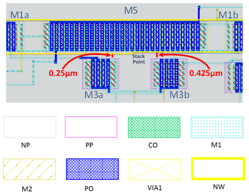 | Figure 2. Nwellstack style of layout of current mirror part in a two-stage OPAMP |
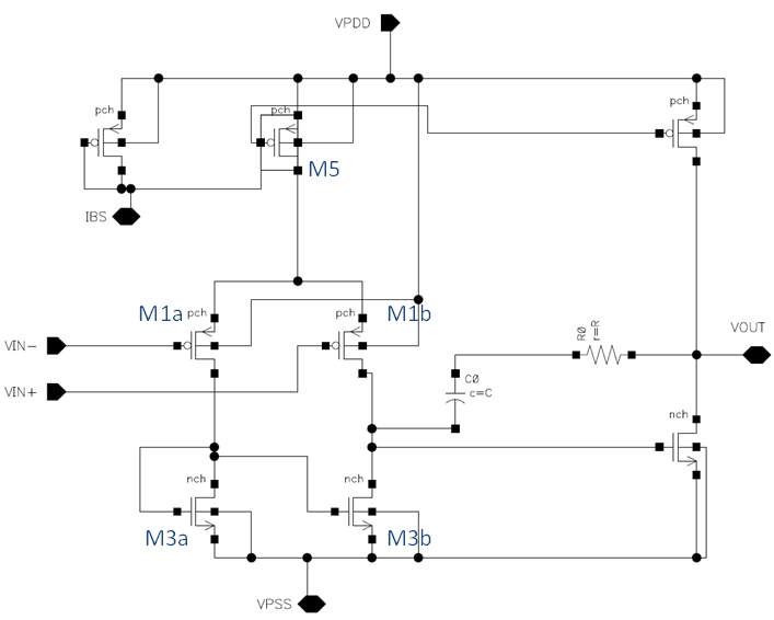 | Figure 3. Schematic of a two-stage OPAMP |
4.2. Impact of STI
- Most of the previous works in the literature only expose the impact of STI on mobility. However, one cannot easily retrieve the factor or indicator of mobility itself. However, one parameter closely related to mobility after simulation can be discovered in equation (7).
 | (7) |
 | (8) |
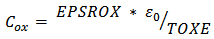
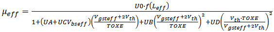
 is permittivity of free space in (8) [33].Calculated μeff can reflect an integral effect leading to mobility variation. WPE can be easily disabled by setting SCA/SCB/SCC = 0. Although STI is not offered with such a flexibility, the effect of STI can be minimized by setting SA/SB large enough. Futhermore, STI may not be accurately reflected for circuit-level simulation as NF is only meaningful in layout-related simulation.Different from μeff, U0 is the low-field surface mobility at nominal oxide thickness tnom. It is provided in any licensed PDK and model according to different bins (or called sections), which are sorted on basis ofMOSFET aspect ratio. Therefore, it is uniform for the devices within the same aspect ratio bin. Commonly speaking, model parameter U0 is kept unchanged regardless of device operation region. From the perspective of physics, once STI is inserted, the model parameter U0 should be re-modeled to reflect STI effect, namely U0_STI for this purpose. As can be seen from (9), by varing SA/SB from very long-distant to any closer locations, one can acquire a pair of operating parameters (Betaeff and Betaeff_STI) from simulations. The ratio exactly reflects the mobility change incurred by STI. By multiplying U0, the U0_STI is obtained.
  | (9) |
 | (10) |
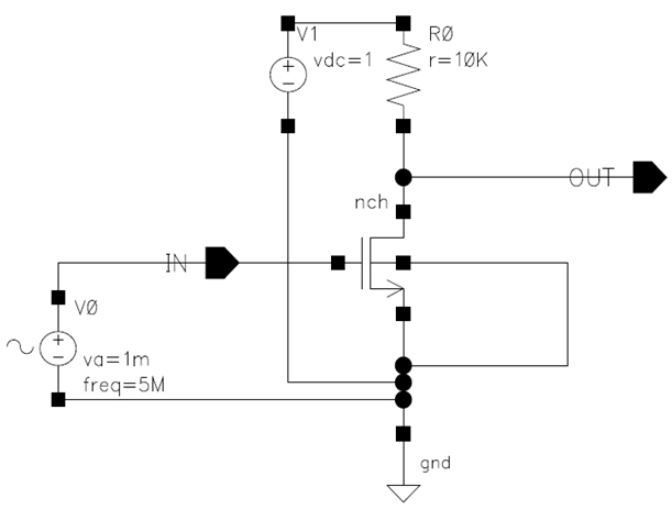 | Figure 4. Schematic of an n-input single stage common-source amplifier |
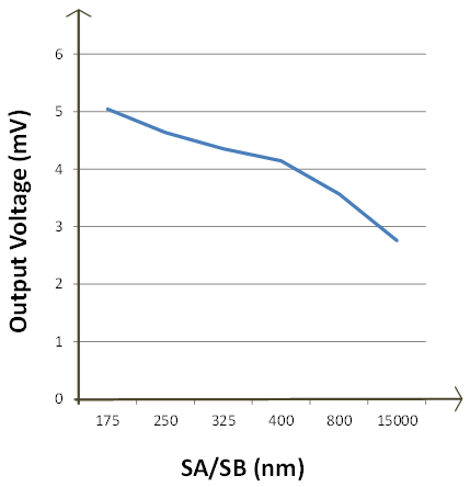 | Figure 5. Output voltage if given 1mV input under different STI effect |
5. Conclusions, Implication, and Future Work
- In this paper, we have reviewed diverse synthesis flows with a focus on layout-aware sizing algorithms. A classification of the related works from the literatures on layout-aware analog circuit sizing is made on the basis of the applied sizing techniques, including stochastic, deterministic, GP/symbolic-analysis-based, or Gm/Id-based approaches. Other categorization criteria, such as the schemes of performance evaluation and layout parasitic estimation, are also discussed. In addition, in this paper we reviewed the existing design automation techniques that take into account LDEs, mainly WPE and STI. We discussed the way how to verify them in the experiments. We also used simple exemplary circuits to demonstrate the significance of WPE and STI with respect to circuit performance. It is expected that 50% of Id variation, 100mV of threshold voltage variation, and 20-30% bias point shift would be even severer without extra consideration of LDEs at the advanced technology nodes.Experiments in Section 4 are sufficient to give analog circuit designers implication that efforts are still needed to address performance influential layout effects at the CMOS 65nm and below technology nodes. Before a full-fledged CAD tool with accurate built-in LDEs models is available for use, analog design would continue to suffer from certain degree of redesign at least for fine tuning and verification. On the other hand, a real layout-aware synthesis flow, which can consider LDEs, is urgently demanded to alleviate the pressure imposed on the analog circuit designers. In our future work, we plan to further investigate S/D oriented and left-side/right-side overlap (LRO) well proximity sub-effects, PSE and OSE in addition to WPE, STI and parasitics. An automatic synthesis flow with LDEs consideration will be developed on the basis of the investigation aforementioned.
ACKNOWLEDGMENTS
- This work was supported in part by the Natural Sciences and Engineering Research Council of Canada (NSERC), Canada Foundation for Innovation (CFI), Research and Development Corporation of Newfoundland and Labrador (RDC), and Memorial University of Newfoundland.