Jean-François Bousquet
Department of Electrical and Computer Engineering, Dalhousie University, Halifax, Canada
Correspondence to: Jean-François Bousquet, Department of Electrical and Computer Engineering, Dalhousie University, Halifax, Canada.
| Email: |  |
Copyright © 2014 Scientific & Academic Publishing. All Rights Reserved.
Abstract
Multicore processing requires highly efficient communication networks for data transmission. In this work, a 10-Gbps wireless communication network is described. The network relies on 16 5-GHz channels in the 300-GHz range and code division multiple access is utilized to share the spectrum among multiple users. A cross-layer design is approached such that the memory content in each core is accessible by partnering cores. A fully-bi-directional transceiver relying on on-off keying is described, an energy efficient transmitter is proposed and each core is expected to consume on the order of 11.43 mW.
Keywords:
Network-on-chip, Track-and-hold comparator, Cross-layer design, Spread spectrum, Sigma-delta converters, On/off keying
Cite this paper: Jean-François Bousquet, A 10-Gbps Energy Efficient On-Chip Wireless Communication Network for Multicore Processing, Microelectronics and Solid State Electronics , Vol. 3 No. 1A, 2014, pp. 9-16. doi: 10.5923/s.msse.201401.02.
1. Introduction
Digitization is overwhelming today’s consumer market and consequently large information sets must be processed rapidly. To decrease processing time over a network of low-power mobile devices, the architecture of the microprocessor must be carefully defined. Commercially available processors now rely on multiple cores that run concurrent threads and allow massive parallel computation. It has been realized though that with the current technology it is difficult to increase the number of cores to more than a few units, because of the cost to exchange information between the cores. The challenge is now to provide a communication medium between the cores. In a traditional network-on-chip such as presented in [1-3], the information is exchanged over busses that are managed by routers. A huge throughput on the order of 100 Gbps is available using 2D mesh networks, but the footprint of the interconnections occupies a significant area of the die. Moreover, on state-of-the-art silicon platforms, the interconnects are lossy and the signal must hence be regenerated using repeaters at regular intervals on the order of a millimeter. More importantly, using a wired infrastructure, a routing mechanism must be in place to ensure that the information can be reached by all cores. The size of the footprint of the processor is significantly increased to allow space for the busses and routers. Fabrication of on-chip optical modulators and waveguides has also received interest to share information between multiple cores [4]. However, Mach Zehnder modulators occupy a large footprint and require significant power consumption, which hinders the possibility to develop on-chip optical networks. In this work, a highly efficient bi-directional wireless communication network is proposed to avoid interconnections between cores. Wireless networks-on-chip have been previously reported to support multicore processing. For example, in [5] a hybrid network architecture in which the 2D wired mesh network is enhanced with wireless routers was described to minimize latency and power consumption. However the details of the front-end circuitry were not discussed. In other work, front-end circuitry is proposed to enable such networks, but there is still a need to detail a complete transceiver architecture that shall enable energy efficient on-chip communication. In this paper, a cross-layer wireless communication protocol is defined and a fully-integrated transceiver architecture is proposed to meet system requirements. The remaining of this paper is organized as follows. In Section 2, a cross-layer communication network designed to reduce the energy consumption is described, in Section 3, a possible transceiver front-end circuitry is proposed, and finally in Section 4 antenna structures are described for inter-core communication.
2. The Communication Network
In this Section, a cross-layer wireless communication standard is proposed to effectively transfer information between multiple cores. In Section 2.1, a wireless communication protocol is defined to share local memory. Then, in Section 2.2 multiple access techniques are described to maximize spectral efficiency. Finally, in Section 2.3 the transceiver architecture is presented.
2.1. Wireless Data Sharing for Multi-Threading
In multi-core processing systems, a protocol must be setup to access the memory shared. In this section a cross-layer network architecture is defined to share the data using a wireless network. As will be shown, compared to a wired infrastructure, the proposed network has two important benefits: 1) latency due to multi-hop transmission is significantly reduced, and 2) interconnections for routing are avoided, thus significantly reducing the footprint. A conventional network-on-chip shown in Figure 1a uses data busses to access local and remote memory and transfer the information from one core to another. However, interconnects in modern CMOS platforms are lossy. To mitigate the deterioration of the RC time constant and coupling interference, a large separation between each line of the bus must be fixed. Because of this, the footprint increases significantly commensurate with the width of the bus. Moreover, a wired infrastructure relies on routers to direct the information to the intended cores [3]. However, packet switching routers require complex processing and must operate at high speed to satisfy the network requirement. Because of this, they are generally power hungry. For example, in 2007 Intel described a 2D mesh network [6] that relies on 5-port routers for multicore processing. To establish an 80 Gbps network, each router consumed almost 1 Watt, and thus required an excessive amount of power for a large number of cores. Instead of using an interconnected network, in this work a wireless network is preferred as shown in Figure 1b. The total throughput that can be achieved between 256 cores on-chip is equal to 10-Gbps and each core-to-core link is configured to transmit at a fixed rate equal to 39.06 Mbps. Although high bitrates on the order of 100 Gbps that have been demonstrated using wired 2D mesh topologies cannot be supported using a wireless network, operations that can be carried out concurrently can benefit from a low-speed wireless network. Moreover, to optimize the performance, careful planning of the core activities can be used to efficiently realize a specific task assigned to the processor. 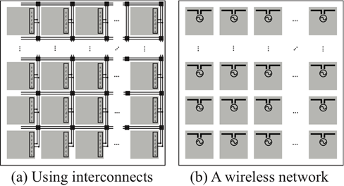 | Figure 1. Representation of the On-Chip Wireless Communication Network between Multiple Cores |
A mechanism is also expected to synchronize between cores for remote memory access. Each core is configured to write to a local memory and can also request to obtain information from remote memory. As in [7], two basic mechanisms exist to allow access: 1) locking of specific memory areas for writing during concurrent access, and 2) queue management to read and write at different memory addresses. To optimize access to memory, we adopt a sophisticated strategy described in [8] in which two types of operations are defined: synchronization and data access. The data access operations are read and write, while synchronization instructions are acquire and release. During an acquire instruction, further data processing is delayed until lock is achieved. A release instruction notifies the completion of previously issued data operations. Finally, to allow the transfer of the memory content, a handshaking protocol shown in Figure 2 is defined. The frame is defined to allow the transfer of large sets of memory content as well as short control messages. Each frame begins with a start sequence, followed by the number of bits, the source identifier, a message identifier and the payload and ends with a parity check. The source identifier defines the originating core for the message, whereas, the message identifier defines the actions to be taken at the receiver communication stack. As shown in Figure 2, when a request is sent from a remote core, memory access is attempted. Upon successful access, the data is framed and returned to the originating core. If the memory is locked, data will not be transmitted and if a timeout occurs at the requesting core, the request is then re-transmitted. 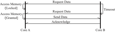 | Figure 2. Example of a handshaking procedure |
2.2. Multiple Access for Wireless
In this section, a methodology is described to maximize the total throughput of a wireless network-on-chip. Spectral resources are managed using a combination of code division multiple access (CDMA) and frequency division multiple access (FDMA). Space-division multiple access (SDMA) cannot realistically be considered for network on-chips because the antenna array footprint would be excessively high. Indeed, for a 300 GHz center frequency and antennas that are spaced by a half-wavelength, the minimum separation between on-chip antennas is equal to 0.5 millimeters for a permittivity of εr = 3.9. Even if we assume each antenna to be a point source, a 4-element linear array would require at least 1.5 mm length which would surpass the footprint of a small processing core. A fully bi-directional communication front-end is adopted, because it allows simultaneous transmission and reception through a common antenna. A fully bi-directional transceiver is chosen to avoid scheduling multiple time slots during each core’s transmission. To avoid excessive self-interference caused by the transmitter on the receiver, an on-chip duplexer isolates the transmitter from the receiver. Potential on-chip duplexer design are described in [9, 10]. Interference cancellation techniques will be used at the receiver’s baseband to mitigate duplexer leakage. In a reconfigurable multicore processor, specific cores exchange information with a pre-defined subset of cores. In this work, for each of these sub-network, a common frequency allocation is designated. Each frequency allocation occupies 5 GHz and a 6-GHz center-to-center frequency separation is provisioned. Thus, 16 channel allocations are provided between 252 and 348 GHz. On each spectrum allocation, multiple links are established between cores. To allow simultaneous transmission, the information is encoded using CDMA signatures as was also described in [11]. For each link, the CDMA signature serves to identify the destination of the message, while the originating core is identified in the payload of the message. Each core communicates to 16 other cores. The unique identifiers are encoded using a spreading sequence. Walsh codes and pseudo-random (PN) sequences encoded on 32 bits are proposed to maximize throughput constrained on the communication performance. Walsh codes provide perfect cross-correlation between the codes when the wireless channel is narrowband, but for multipath channels PN sequences are preferred because of their good auto-correlation properties.
2.3. Bi-Directional Transceivers
In this section, the architecture of the transceiver associated with each core is described. To minimize overall energy consumption, a cross-layer design that implements the core functions of the OSI stack is utilized. This minimizes overhead in memory utilization and redundant processing. The transceiver is intended to be developed on a state-of-the-art CMOS platform that includes the digital circuitry as well as high-frequency mixed-signal circuitry and mm-wave front-ends. The transceiver architecture is shown in Figure 3.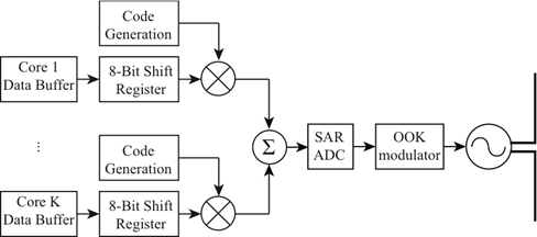 | Figure 3. Block Diagram of the Transceiver |
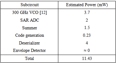
To minimize the front-end complexity, a non-coherent on-off keying (OOK) modulation scheme is chosen. Using OOK, the oscillator is enabled when a logic “1” is transmitted, while it is disabled when a logic “0” is transmitted. At the receiver, an envelope detector measures the amplitude at the carrier frequency to distinguish between the two signal levels. For transmission, the frame content is preliminarily loaded from an 8-bit memory. Upon request, it is serially transmitted using serial shift registers and spread using a unique CDMA signature for each destination core. The spread sequence output chip rate is 1.25 Gsps. An adder is used to sum the output of all streams. This operation generates a multi-level signal amplitude. Because OOK is a binary modulation scheme, the 4-bit output of the 1.25 Gsps adder must be converted to a binary stream operating at 5 Gsps prior to modulation. On-chip antennas have been studied in recent years, and although their efficiency is poor, this is not a major concern for wireless network on-chips since the propagation distance is very short. For 300 GHz transmission, electrically small antennas have a reasonable footprint, and can overlap over the digital circuitry. The antenna is connected to the transceiver using a duplexer that isolates the transmitter and receiver. Discrete circulators are typically implemented using ferrite cores. However, couplers using only passive components have previously been designed [9, 10] and configured to act as on-chip duplexers. The use of OOK also reduces significantly the receiver complexity. Because OOK is a non-coherent modulation technique, the carrier phase recovery is not required, thus avoiding the use of a phase locked loop. As shown in Figure 3 a simple envelope detector is used to demodulate the information. Through a de-serializer, the output of the OOK demodulator is converted to a multi-level signal that represents the summation of all CDMA encoded streams in the network. The output of the de-serializer is multiplied with the CDMA code r and integrated, where r is a unique identifier for each core. The frame is further un-bundled and applied to the core receiver data buffer. Depending on the nature of the message, the receiver will forward the messages to the core processor and acknowledge the message from the transmitter. The wireless network is intended to provide communication at a relatively low energy consumption. The power budget for the sub-circuit of each core is summarized in Table 1. The VCO power is estimated using a previous design described in [12], while the SAR ADC power consumption is extracted from [14]. To calculate the summer power consumption, as will be shown in Section 3.2, the design relies on 15 differential amplifiers that is assumed to be biased with a 100-uA tail current and supplied by a 1-V supply voltage. The code generation power consumption is calculated using P = CloadVdd f2 using a rough estimate of the number of gates required to generate a ring counter for each code. The de-serializer power consumption is calculated assuming a 5-bit current steering DAC and because it consists solely of passive components, the envelop detector is not expected to burn power. Effectively, with an 11.43-mW DC power per core and for a transmission rate of 10 Gbps between the 256 cores, the energy consumption per bit is expected to be on the order of 293 pJ.Table 1. Transceiver Power Budget
 |
| |
|
3. Data Transmission
In this Section, the transmitter circuitry is described to convert the binary information and generate the input signal to the antenna. In Section 3.1, details of a code generation circuit designed using mixed-signal techniques are provided. Further, in Section 3.2, a high-speed adder is described and in Section 3.3 a successive approximation circuit ADC to serialize the input to the antenna is shown. Finally, in Section 3.4 an OOK modulator that generates a gated 300-GHz oscillation is described.
3.1. Code Generation
In this section, two alternative mixed-signal circuits are described to generate a CDMA code. First, in Section 3.1.1 a pulse density modulator is implemented using a sigma / delta architecture. This circuit can serve to generate a random sequence of bits. Second, in Section 3.1.2, Walsh codes are generated using a ring counter that is pre-set with a unique input value.
3.1.1. Pulse Density Modulator
In this section, a pulse density modulator (PDM) is used to generate pseudo-random sequences. The PDM relies on a second order sigma/delta architecture described in [13]. The PDM is shown in Figure 4. The input signal is a digital value encoded on 5 bits using 2s complement representation. A second order implementation of the sigma-delta modulator is preferred to a single order, because it reduces correlation between the codes, and it does not require excessive oversampling [13]. In order for the PDM output to generate a specific sequence, the sigma-delta modulator is reset. After the reset is de-asserted, a window of 32 chips sampled at 1.25 Gsps represents the PN sequence. 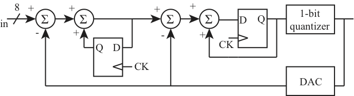 | Figure 4. Sigma Delta Converter |
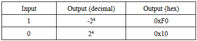
A second order delta-sigma modulator is built using two cascaded stages of modulation. For each stage, the error between the input and the quantized output is integrated over multiple clock cycles. A 1-bit quantizer generates the output binary stream. In the feedback chain, the quantized output is re-converted to a 5-bit digital value using a DAC. The output of the DAC is compared to the input signal of each stage and represents the quantization error. A set of codes is chosen that will have low cross-correlation values. Among the set of possible values bounded between [-31, 32], the 16 codes chosen are positive and limited between [0, 15]. This limits the duty cycle between 50% and 75%. Negative values are not selected because the output code is simply the complement of the positive code and thus highly correlated with it. Moreover, duty cycles relatively close to 50% are preferred to maintain relatively close number of zeros and ones. It is found through simulation that the maximum cross-correlation between codes is 0.4. The DAC conversion from an input bit value to a 5-bit analog output is shown in Table 2. As can be seen, only the MSB of the DAC output changes, thus minimizing hardware complexity. Table 2. ΣΔ DAC conversion table
 |
| |
|
The sigma-delta is implemented using 8-bit adders and subtractors. This avoids any possibility of overflow. To minimize area, ripple carry adders can be used. However assuming a worst case propagation delay on the order of 100 psec for each half adder, the maximum time required for adding 8-bit inputs is 700 psecs and, for a 1.25-GHz clock, it cannot meet the timing requirement, albeit by a small margin. Consequently, to reduce the maximum propagation delay for the addition, a carry lookahead architecture is a preferred choice.
3.1.2. Ring Counter with Preset
As an alternative to a pulse density modulator, it is also possible to generate a set of Walsh codes using a low-complexity shift register configured as a ring counter, as shown in Figure 5. A periodic output pattern is produced, after having preset the input in each stage of the shift register. In absence of multipath, the Walsh code presents perfect cross-correlation properties, which is an advantage compared to the pseudo-random code. However, its performance degrades in multipath environments, in which case, the PN sequence is preferred.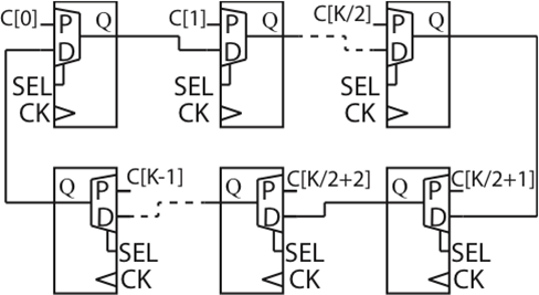 | Figure 5. Ring counter |
The ring counter maximum frequency is limited by the presetable shift register access time, defined as the delay at which the output data is valid after the clock event is asserted. Also, for a 32-bit Walsh code, the clock line fanout is very large. Careful routing of the clock signal and adequate loading is necessary to ensure that hold time is met for extreme process variations. Under these careful design procedures, and for a relatively low clock frequency of 1.25 GHz, typical standard cells in modern CMOS technology provide more than sufficient timing margin.
3.2. High-Speed Adder
At the transmitter, the output of each CDMA spreading operation must be summed together to allow simultaneous transmission. There is a maximum of 16 spreading codes to be summed, and because of the randomness of the code, codes can be chosen such that their summation at each chip period never exceeds an integer value between [-7, 8]. For this reason an adder that can represent a value on 4 bits is required. Different circuit architectures can be considered. Multi-bit adders can be used to produce a digital word that can then be converted to an analog value, using for example a current steering DAC. As was the case for the PDM, a carry lookahead architecture can be considered. However, the total area including the current mirrors for the DAC is disadvantageous.Instead, in this work each adder shown in Figure 6 uses a track-and-hold comparator. A priori, the digital output of the spreading circuit is converted to a differential signal with a controlled common mode voltage. The track-and-hold comparator is shown in Figure 7. A differential structure is chosen to reduce the 2nd order nonlinearity. For simplification purposes, a single-ended analysis of the circuit is explained for the left-hand side of the circuit. A similar analysis can be done on the right. During phase φ2, the input to the differential pair is forced to zero, and the voltage in the capacitor is set to vin2-. Then, during phase φ1, the input signal to the capacitor is vin1+, and because the voltage across the capacitor cannot change instantaneously, the input to the differential pair is vin1+ - vin2-. To minimize area, the size of the capacitor should be as small as possible, while maintaining a time constant much greater than the clock period. For this technology, the chosen capacitor value is on the order of 10 fF to 100 fF.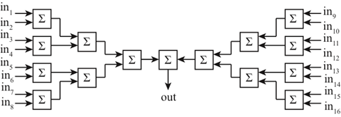 | Figure 6. Cascading of 2-bit adders to minimize summer latency |
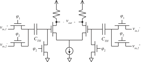 | Figure 7. Summer using capacitive transfer of energy |
The differential input to the amplifier is (vin1+ - vin2-)-(vin1- - vin2+), and for an amplifier gain A, the output is A((vin1+-vin1-)+(vin2+−vin2-)).To maintain a 1.25 GHz chip rate, the summation operation must be completed within the chip duration. The chip period is divided into 4 windows. After the first window, the first adder stage output is valid and is used by the second adder stage, and so on. At the end of the fourth window the summation operation is complete. The clock alignment to control the stages is shown in Figure 8. Using a 5 GHz input clock, four pulses ckth1−ckth4 are generated that control φ1/φ2 for each track-and-hold stage. The pulse is delayed by one cycle for the control of each subsequent adder. When the pulse is high, the addition operation is reset and when it is low, the adder output is ready.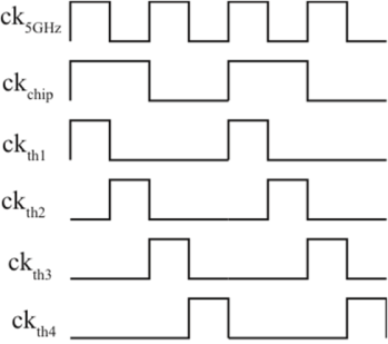 | Figure 8. Alignment of the track-and-hold clocks |
3.3. Successive Approximation Register ADC
A serializer that converts a 4-bit word to a binary stream sampled at 5 Gsps is required at the output of the summer to send the digital information. A successive approximation register (SAR) ADC is chosen to achieve this requirement. In a SAR ADC, a binary search uses multiple clock cycles to determine the closest digital word to match to the input signal.As shown in Figure 9, the SAR ADC requires a single comparator, a bank of capacitors, as well as a 5-GHz polyphase clock. During the sample phase, the signal is shorted to the input of the capacitor array, while the input to the comparator is forced to zero. Further, during the hold mode, the input to the capacitors is flipped to ground. Then, during the bit cycling period, the input to the capacitors are individually toggled to Vref, thus defining the sequence of bits transmitted. A SAR ADC operating in this range of frequencies has been demonstrated in [14]. | Figure 9. Successive Approximation Register ADC to serialize the transmitter output |
3.4. On/Off Keying
To generate OOK keying, the carrier oscillator is simply enabled when the input bit is high and disabled when it is low. This type of circuit has been implemented using low-energy consumption in [15] and it is shown that the power supply can be modulated to activate the oscillator. For each core to synthesize to the 16 possible channels, a voltage controlled oscillator (VCO) design is required. Although a 300-GHz VCO is a challenging circuit to design and measure, recent reports demonstrate their feasibility [16, 12]. Also, in [17], an OOK keying modulator controls a 260 GHz oscillator for chip-to-chip communication. A quadrupler is used to generate the local oscillator. Note that the oscillator must be connected to the on-chip duplexer though a buffer with a matched load.
4. On-Chip Antenna and Duplexer
The on-chip transceiver includes a duplexer and an integrated antenna, both circuits consisting of relatively large passive components on the upper metal layers. Although on-chip antennas have been known to suffer from poor efficiency on the order of 10%, shielding techniques exist to improve the gain of the antenna. For example, Niknejad’s group at Berkeley characterized a 260-GHz wireless link [17] using an on-chip leaky wave antenna in 2012. The antenna efficiency was evaluated to be 26%. For this efficiency and an input power at the transmit antenna equal to −10 dBm, a 56-dB free space propagation loss over a 5-cm maximum distance link, the receiver input power is at a respectable level above −78 dBm. Also, a duplexer can be implemented using an integrated circulator. In [9], the two topologies shown rely on a passive coupler attached to identical loads. As an alternative, an on-chip duplexer design using a set of transformers is described in [10].
5. Conclusions
In this work, a 10-Gbps wireless network-on-chip has been proposed to enable communication between 256 processing cores. A cross-layer design has been discussed to reduce hardware overhead. It includes the communication protocol to access remote memory, and a multiple access technique that combines spread spectrum technology with frequency division multiplexing. To enable a 10-Gbps wireless network, 16 5-GHz channels are provisioned in the 300-GHz frequency range. At each core, a fully bi-directional transceiver relying on-off keying to minimize energy consumption has been described and a power budget of 11.4 mW per core has been estimated.
References
| [1] | S. Vangal et al. “An 80-Tile 1.28TFLOPS Network-on-Chip in 65nm CMOS.” In IEEE Intl. Solid-State Circuits Conf., 2007., pages 98–589, Feb 2007. |
| [2] | S. Bell et al. “Tile64 - processor: A 64-core soc with mesh interconnect.” In IEEE Intl. Solid-State Circuits Conf., 2008, pages 88–598, Feb 2008. |
| [3] | M.A Anders, H. Kaul, S.K. Hsu, A Agarwal, S.K. Mathew, F. Sheikh, R.K. Krishnamurthy, and S. Borkar. “A 4.1Tb/s bisection-bandwidth 560Gb/s/W streaming circuit-switched 8×8 mesh network-on-chip in 45nm CMOS.” In Solid-State Circuits Conference Digest of Technical Papers (ISSCC), 2010 IEEE International, pages 110–111, Feb 2010. |
| [4] | M. Haurylau et al. “On-chip optical interconnect roadmap: Challenges and critical directions.” IEEE J. Sel. Topics Quantum Electronics, 12(6):1699–1705, Nov 2006. |
| [5] | Chifeng Wang, Wen-Hsiang Hu, and N. Bagherzadeh. “A wireless network-on-chip design for multicore platforms.” In 19th Euromicro Intl. Conf. Parallel, Distributed Network-Based Process., 2011, pages 409–416, Feb 2011. |
| [6] | S. Vangal et al. “A 5.1-GHz 0.34-mm2 Router for Network-on-Chip Applications.” In IEEE Symp. VLSI Circuits, 2007, pages 42–43, June 2007. |
| [7] | D. Pasetto et al. “Performance Evaluation of Inter-thread Communication Mechanisms on Multicore/Multithreaded Architectures.” In Proceedings of the 21st International Symposium on High-Performance Parallel and Distributed Computing, HPDC ’12, pages 131–132. ACM, 2012. |
| [8] | A Naeem, A Jantsch, and Zhonghai Lu. “Scalability analysis of memory consistency models in NoC-based distributed shared memory SoCs.” IEEE Trans. Comput.-Aided Design Integr. Circuits Syst., 32(5):760–773, May 2013. |
| [9] | D. Ozis, J. Paramesh, and D.J. Allstot. “Integrated quadrature couplers and their application in image-reject receivers.” IEEE J. Solid-State Circuits, 44(5):1464–1476, May 2009. |
| [10] | M. Mikhemar, H. Darabi, and AA Abidi. “A Multiband RF Antenna Duplexer on CMOS: Design and Performance.” IEEE J. Solid-State Circuits, 48(9):2067–2077, Sept 2013. |
| [11] | Daewook Kim, Manho Kim, and G. E. Sobelman. “CDMA-based network-on-chip architecture.” In 2004 IEEE Asia-Pacific Conf. Circ. Syst., volume 1, pages 137–140 vol.1, Dec 2004. |
| [12] | B. Razavi. “A 300-GHz Fundamental Oscillator in 65-nm CMOS Technology.” IEEE J. Solid-State Circuits, 46(4): 894–903, April 2011. |
| [13] | B.E. Boser and B.A Wooley. “The design of sigma-delta modulation analog-to-digital converters.” IEEE J. Solid-State Circuits, 23(6):1298–1308, Dec 1988. |
| [14] | P. Schvan et al. “A 24GS/s 6b ADC in 90nm CMOS.” In 2008 IEEE Intl. Solid-State Circuits Conference, pages 544–634, Feb 2008. |
| [15] | M. Crepaldi, Chen Li, J.R. Fernandes, and P.R. Kinget. “An Ultra-Wideband Impulse-Radio Transceiver Chipset Using Synchronized-OOK Modulation.” IEEE J. Solid-State Circuits, 46(10):2284–2299, Oct 2011. |
| [16] | Ho-Jin Song, Jae-Young Kim, K. Ajito, M. Yaita, and N. Kukutsu. “Fully Integrated ASK Receiver MMIC for Terahertz Communications at 300 GHz.” IEEE Trans. THz Science Tech., 3(4):445–452, July 2013. |
| [17] | Jung-Dong Park, Shinwon Kang, S.V. Thyagarajan, E. Alon, and AM. Niknejad.” A 260 GHz fully integrated CMOS transceiver for wireless chip-to-chip communication. “In 2012 Symp. VLSI Circuits, pages 48–49, June 2012. |
 Abstract
 Reference
 Full-Text PDF
 Full-text HTML