-
Paper Information
- Next Paper
- Previous Paper
- Paper Submission
-
Journal Information
- About This Journal
- Editorial Board
- Current Issue
- Archive
- Author Guidelines
- Contact Us
Microelectronics and Solid State Electronics
p-ISSN: 2324-643X e-ISSN: 2324-6456
2014; 3(1A): 1-8
doi:10.5923/s.msse.201401.01
Guideline on Quantitatively Analyzing Analog Nano-Scale CMOS Circuits Using Ultra-Compact Model
 Abstract
 Reference
 Full-Text PDF
 Full-text HTML
Haoran Yu, Kamal El-Sankary, Ezz El-Masry
Department of Electrical and Computer Engineering, Dalhousie University, Halifax, Canada
Correspondence to: Haoran Yu, Department of Electrical and Computer Engineering, Dalhousie University, Halifax, Canada.
| Email: |  |
Copyright © 2014 Scientific & Academic Publishing. All Rights Reserved.
This paper presents a tutorial about analyzing analog nano-scale CMOS circuits quantitatively. A ultra-compact model which is numerically accurate is essential in the analysis. Besides, the characteristics of nano-scale MOSFET must be considered. The nonlinear output conductance and the cross-terms among the controlling voltage cannot be ignored in nano-scale circuits. Distortion analysis of nano-scale gate-driven and bulk-driven amplifier is performed as a demonstration of this guideline.
Keywords: CMOS, Bulk-driven, Distortion, Model
Cite this paper: Haoran Yu, Kamal El-Sankary, Ezz El-Masry, Guideline on Quantitatively Analyzing Analog Nano-Scale CMOS Circuits Using Ultra-Compact Model, Microelectronics and Solid State Electronics , Vol. 3 No. 1A, 2014, pp. 1-8. doi: 10.5923/s.msse.201401.01.
Article Outline
1. Introduction
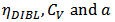
- Owing to the reducing channel length of metal – oxide – semiconductor field-effect transistor (MOSFET), the performance of complementary metal-oxide-semiconductor (CMOS) integrated circuits (IC) has been improved greatly, such as power consumption, speed and noise [1-3]. Meanwhile, bulk-driven (BD) technique has been proposed to tackle the harsh voltage-swing challenge in modern low voltage design [4]. BD MOSFET works in a depletion mode which allows negative, zero and small positive bias voltage at the bulk terminal. This technique increases the input common mode range as well as the signal swing, which cannot be realized by gate-driven (GD) technique at low VDD [4].To design high performance nano-scale GD/BD circuits, quantitative analysis is necessary. In order to analyze nano-scale circuits quantitatively, firstly, a current model which characterizes transistor accurately is demanded. Especially for BD circuits, the model must be also accurate when the signal is applied at the bulk-terminal.To describe the characteristics of nanometer MOSFET, several physic effects have to be included into model, such as the short-channel (SCE) and the narrow width effect (NWE), the mobility degradation (MD), the velocity saturation (VS), the channel-length modulation (CLM), the drain-induced barrier lowering (DIBL) and the source-drain parasitic resistance (S/D-PR) [5]. Berkeley short-channel insulated-gate model (BSIM) [6] provides the highest accuracy; however, it has a large number of parameters and is the most complex model which is simulation-oriented, not suitable for circuit analysis. Comparing with simulation-oriented model, ultra-compact model is more ideal to be applied to analyze circuit [5]. Models can be also selected according to the type of analysis, i.e. qualitative or quantitative analysis. For qualitative analysis, simple model can be used as long as it shows the characteristics of MOSFET in the targeting operational region qualitatively accurately. For example, the model from [7] that covers the subthreshold and moderate inversion regions was successfully applied to analyze the mixing mechanism of BD mixer and new application of BD mixer has been found based on the analysis [8]. For quantitative analysis, such as the numerical calculation of distortion of nanometer GD/BD circuits, ultra-compact model which is numerically accurate for nano-scale MOSFET must be chosen. Reference [5] provides such a model which has ten parameters and is accurate for nanometer MOSFET; however, it was originally proposed to digital applications, not optimized for bulk-driven applications. In this work, the model is modified to be adapted to the characteristics of nano-scale BD transistor. Hence it can be applied to quantitatively analyze BD circuits.Besides the model selection/adaption, the characteristic of nano-scale MOSFET must be also considered in the analysis. In this research, it is found that the nonlinear output conductance and the cross-terms play important roles in the analysis, although they are often ignored in the analysis of mirco-scale CMOS circuits.The paper is organized as following. In Section 2, the original model is introduced and modified for BD applications. The results of parameter extraction and fitting are illustrated. The parameters of the model are fitted well with the simulation data which is the premise of the analysis. Section 3 shows the importance of the inclusion of the nonlinear output conductance and the cross-terms. The distortion analysis of GD/BD RF amplifier is demonstrated as an example of this guideline. Finally there is a brief conclusion in Section 4.
2. Accurate Current Model for Nano-Scale MOSFET and Its Modification for BD Applications
2.1. Original Current Model
- By combining the merits of the previous ultra-compact models [9-12], and by including DIBL, NWE, and S/D-PR, a 10-parameter model was proposed for nano-scale CMOS transistor in [5]:
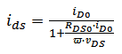 | (1) |
 | (2) |
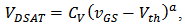 | (3) |
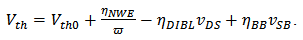 | (4) |
 and
and  are used to linearly proportionally scale current and saturation voltage; n and a are used to describe the fractional power dependence of the current and the saturation voltage on the overdrive voltage
  ; body biasing (BB), DIBL, and NWE are described by adding corrective terms
 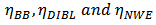 into
into  ; the transistor width is referred as is the multiple,
  , of the minimal allowed width;
  is used to describe the impact of S/D-PR;
  is the coefficient of CLM.This model describes the I-V characteristics accurately in superthreshold region [5]. However, it was originally proposed to digital applications, not optimized for BD applications. In order to perform the quantitative analysis of BD circuits, it is modified in this work to adapt to BD MOSFET and the parameters are fitted to a commercial 65 nm technology used in this research.
 2.2. Modified Model for BD Applications
- To investigate if the model can describe the characteristics of nano-scale MOSFET accurately, I-V characteristic needs to be examined. Furthermore, up-to-three order of derivatives
 of
of  over bias voltages have to be fitted.
  is defined as:
 Obviously,
 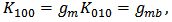 and
and  , which are the first-order coefficients of the nonlinear (bulk-) transconductance and the nonlinear output conductance, respectively.
 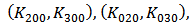 and
and  are second- and third-order nonlinear coefficient only related to
  ,
,  , and
, and  , respectively. Others are the coefficients of the cross-terms among
  ,
,  , and
, and  .In strong inversion region,
  are the most effective parameters to adjust
  and
and 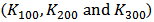 versus
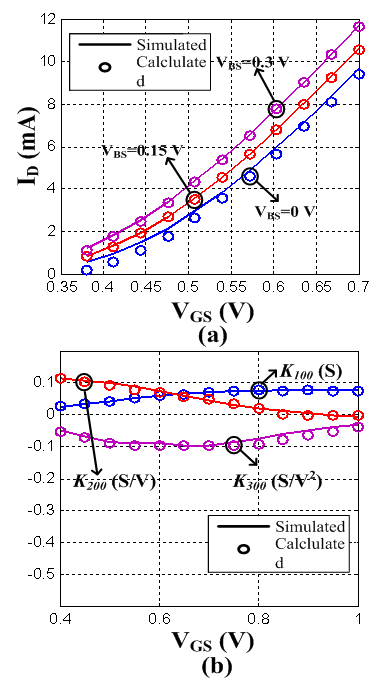
  . Figure 2 shows the results of parameter fitting. Figure 2 (a) shows the drain current
  versus
  when
when  . Figure 2 (b) shows
  versus
  when
when  and
and  . The simulation data are obtained from a transistor of
 , using BSIM 4 model; The simulation test bench is shown in Figure 1.
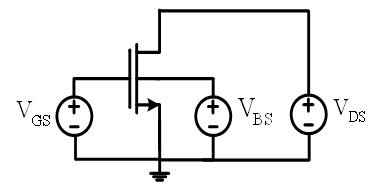 | Figure 1. Simulation test bench |
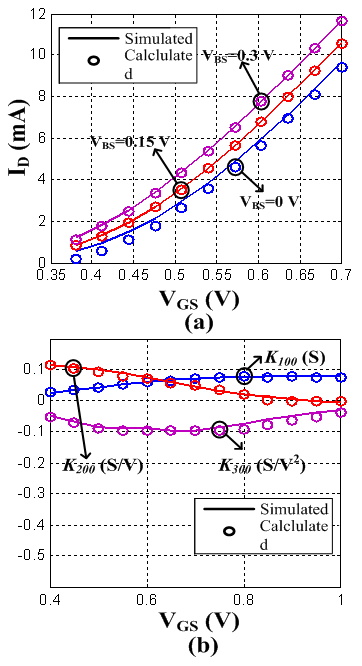 | Figure 2. Comparison between the simulated and calculated  and and 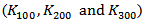 versus versus  |
 and (
and ( ) versus
  are mainly controlled by the parameters of
  ,
,  in saturation region. Figure 3 demonstrates the comparison of
  and (
and ( ) versus
  . In Figure 3 (a),
  . In Figure 3 (b)
  and
and  . From Figure 2 and Figure 3 show that good fitting of
  and its derivatives over
  and
and  are achieved.In the original model,
  and
and  are basically adjusted by
  . It is found for the original model in [5] that even if the calculated
  are close to the simulated values,
  and
and  are still underestimated. And if
  and
and  are adjusted to be close to the simulated ones,
  are apart from the simulated values. It is proposed that
  is added to the current model to adjust
  and
and  without affecting
  :
: | (5) |
 | Figure 3. Comparison between the simulated and calculated  and and 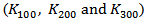 versus versus  |
 and
and  versus
  . In Figure 4 (a),
  . In Figure 2 (b),
  and
and  . It is clear that without this added parameter,
  and
and  are underestimated. This added parameter gives us one more degree of freedom to achieve accurate fitting of both linear and nonlinear terms.
 | Figure 4. Comparison between the simulated and calculated  and and  versus versus  |
 ,
,  is still underestimated (as shown in Figure 2 (a), Figure 3 (a), and Figure 4 (a)) and
  is a little overestimated (as shown in Figure 4 (4)), the fitting parameters can give us reasonable accuracy in quantitative analyses. A current model which is fitted to the used technology accurately is the prerequisite of numerically analyzing nano-scale CMOS circuits.
3. Quantitative Analysis of Nano-Scale Circuits
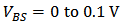
- In Section 2, the model proposed in [5] has been modified for BD transistor; and its parameters have been fitted well. Hence it can be applied to analyze nano-scale CMOS circuits quantitatively, e.g. the distortion analysis of GD and BD amplifier (see Figure 5). The goal of quantitative distortion analysis is to achieve mathematical expressions of the distortions which can predict the nonlinear behavior of the GD/BD amplifier. Using the modified current model in which the parameters are extracted and fitted to the CMOS technology, the bias voltages can be applied as inputs of the expressions of distortions, and the distortions can be acquired as the outputs [13-15].
 | Figure 5. Schematic of GD amplifier (a), and BD amplifier (b) |
 ,
,  and
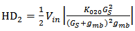
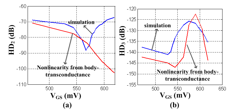
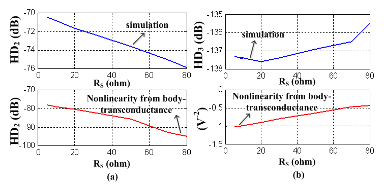
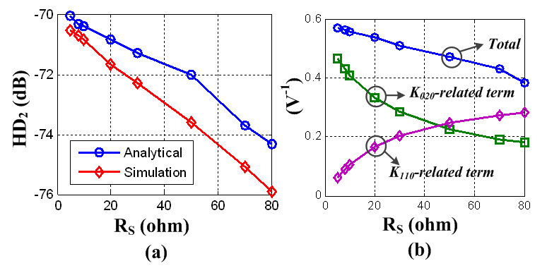
and  . The the expression of HD2 and HD3 of the GD and BD amplifier can be found in [14, 15], respectively.From Figure 6, it is clear that there is significant error between the simulated and the calculated second-order and third-order harmonic distortion (HD2 and HD3) if only the nonlinearity of the transconductance is considered in the analytical calculation. The calculation cannot even predict the trend of behavior of HD. It is also found that the effect of the source degeneration resistance (RS) depends on the bias point in this study. Under certain bias condition, the increase of RS cannot reduce HD monotonically, as shown in Figure 7, where the bias current is 3.2 mA. However, if the contribution from the nonlinear output conductance and the cross-terms is excluded, the nonlinear term only from the transconductance is reducing continuously with RS, i.e. the value of
  and
and 
 .
. 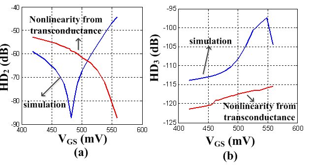 | Figure 6. Comparison of the simulated HD2 (a) and HD3 (b) versus VGS of thenano-scale GD amplifier with the calculated HD which only includes the nonlinearity of the transconductance |
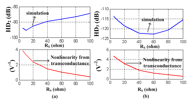 | Figure 7. Comparison of the simulated HD2 (a) and HD3 (b) versus the source degeneration resistance of a nano-scale GD amplifier with the calculated HD which only includes the nonlinearity of the transconductance |
 is expected if only the nonlinearity from the body-transconductance is considered; however, only about 6 dB reduction is obtained by simulation. For HD3, simulation shows that at this bias condition (the bias current is 2.5 mA), RS cannot be used to reduce HD3; however, calculation of the term that only includes the nonlinearity of the body-transconductance, i.e.
 shows an opposite change of HD3 with RS, as shown in Figure 9 (b). Here,
  .
. | Figure 8. Comparison of the simulated HD2 (a) and HD3 (b) versus VGS of thenano-scale GD amplifier with the calculated HD which only includes the nonlinearity of the transconductance |
 | Figure 9. Comparison of the simulated HD2 (a) and HD3 (b) versus the source degeneration resistance of a nano-scale GD amplifier with the calculated HD which only includes the nonlinearity of the transconductance |
 increases continuously. Besides, when
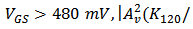

 increase substantially and become the major parts of
  ; also, the last one has opposite sign against the first two, thus the total of them, i.e.
  , shows the characteristic shown in Figure 10. Here,
  ,
,  is the output conductance and
  is the load. From Figure 11 (b), it is realized that although the amplitude of the
  and
and  -related term is monotonically reduced by
  , the amplitude of the
  ,
,  , and
, and  related terms is parabola, especially the
  related term becomes the major part when
  . Thus, the total of all the terms in
  behaves as parabola and starts increasing when
 .
.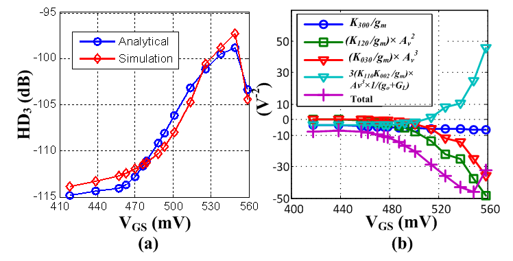 | Figure 10. (a) Analytical and simulated  , and (b) , and (b)  , three other major contributions, and the sum of all the terms in HD3 , three other major contributions, and the sum of all the terms in HD3 |
 | Figure 11. Effect of  : (a) the analytical and simulated : (a) the analytical and simulated  ; (b) the contribution of the dominantterms to ; (b) the contribution of the dominantterms to  under 3.2mA bias current under 3.2mA bias current |
 contributes less as VGS increases; however,
 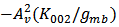 increases significantly when
 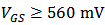 , thus
  is increased. Moreover, the contribution of
  cancels that of
 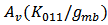 since they have the same sign and subtract each other. The values of the two terms are equal around
 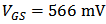 , hence there is an optimal region of
  . Figure 13 (b) demonstrates the contribution of
  and
and  -related terms in HD2. Although
  contributes less as well known in long channel technology, the contribution of
  -related term increase significantly and counteract against the reduction of
  -related term. Thus
  reduces slower as
  increases.By following this guideline, i.e. using an quantitatively accurate model and including the nonlinear output conductance and the cross-terms, HD2 of the GD amplifier and HD3 of the BD amplifier can be calculated correctly and each term in the expressions of HD2/HD3 can be analyzed to interpret the characteristic.
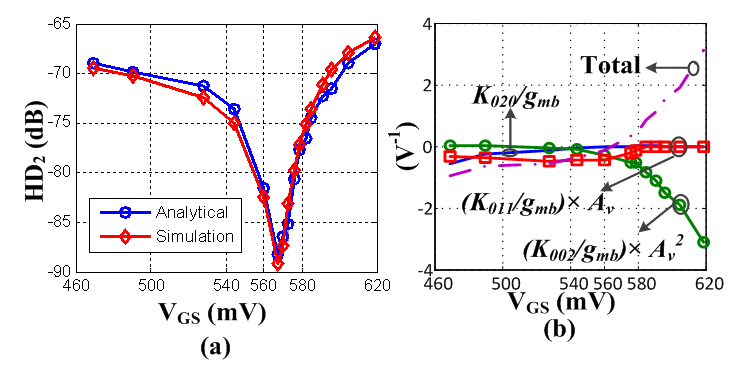 | Figure 12. (a) Analytical and simulated  when when  , and (b) the contribution of each term and the sum of all the terms in HD2 , and (b) the contribution of each term and the sum of all the terms in HD2 |
 | Figure 13.  related terms in HD2 and the total of all the terms in HD2 versus related terms in HD2 and the total of all the terms in HD2 versus  under 2.5mA bias current and under 2.5mA bias current and  |
4. Conclusions
- The guideline of quantitatively analysing nano-scale CMOS circuits can be summarized as: First, anultra-compact model which is numerically accurate for nano-scale MOSFET is required. The parameters in the model have to be fitted the used technology. One of these kinds of models is introduced in this paper, which is modified here to be adapted to BD applications by introducing one new parameter to achieve accurate fitting of both linear and nonlinear terms. This modified model can be applied for analysing nano-scale GD/BD circuits. Second, for nano-scale CMOS circuits, the nonlinear output conductance and the cross-terms among the controlling voltages, i.e.
 ,
,  , and
, and  , must be included; otherwise there would be significant error between the calculated and simulated results.In this paper, the distortion analysis of nano-scale GD and BD amplifier is demonstrated as an example to show the importance of the nonlinear output conductance and the cross-terms, as well as the effectiveness of the accurate ultra-compact model.