Vasantha Kumar B.V.P1, N.S. Murthy Sharma2, K. Lal Kishore3, A. Rajakumari4
1Design Consultant, Global Technical Services, Synopsys Inc., Hillsboro, OR, USA
2Department of Electronics and Communications, BVCE College, Odalarevu, India, 533210, India
3Department of Electronics and Communications, J.N.T.U.A, Ananthapur, 515002, India
4Department of Electronics and Communications, B.V.R.I.T, Narsapur, 502313, India
Correspondence to: Vasantha Kumar B.V.P, Design Consultant, Global Technical Services, Synopsys Inc., Hillsboro, OR, USA.
| Email: |  |
Copyright © 2012 Scientific & Academic Publishing. All Rights Reserved.
Abstract
This paper proposes a glitch compensation technique which involves reducing glitch power in selected combinational cells to reduce peak current which contributes to dynamic voltage or IR drop. The proposed methodology can be seamlessly integrated to existing physical design flows. A glitch is an undesired transition that occurs before intended value in digital circuits. A glitch occurs in CMOS circuits when differential delay at the inputs of a gate is greater than inertial delay, which results into increased gate switching and hence notable amount of power consumption. When such large number of logic gates switch close to the same time they will contribute to power integrity challenge called peak dynamic IR drop. The glitch power is becoming more prominent in lower technology nodes. Introduction of buffers at the input of the Logic gate may reduce glitches, but it results into large area overhead and dynamic power. In the proposed methodology we are using transmission gate as a compensation circuit to reduce extra leakage and dynamic power. A flow is proposed for charactering the pass transistor logic to cater different delay values. The proposed methodology has been validated on a place and routed Multiply Accumulate (MAC) layout implemented using Synopsys SAED 90nm Generic library. Experimental results show 12% to 50% reduction in top 10 peak transient IR drop numbers with just 12% glitch power reduction in selected combinational cell instances. When compared to traditional on-chip decoupling capacitor (Decap) cells insertion method the proposed technique could reduce the peak IR drop numbers by the same amount with just 5% increase in total core capacitance.
Keywords:
Dynamic Power, Glitch Power, Switching Activity, IR Drop, Decoupling Capacitance
Cite this paper: Vasantha Kumar B.V.P, N.S. Murthy Sharma, K. Lal Kishore, A. Rajakumari, Selective Glitch Reduction Technique for Minimizing Peak Dynamic IR Drop, Microelectronics and Solid State Electronics , Vol. 2 No. A, 2013, pp. 27-32. doi: 10.5923/s.msse.201302.04.
1. Introduction
The power spent in Complementary metal oxide semiconductor (CMOS) can be classified as dynamic power consumption and leakage or static power consumption. Leakage power is consumed at all times even in ideal states and it is dominating total power equation in advanced technologies. It is unnecessary and need to minimize it. On the other hand dynamic power consumption is due to the low impedance path between the rails formed through the switching devices. The switching at the output of logic gates can be due to desired functional transitions or due to spurious transitions called glitches. The glitches at the output of logic gates are due to differences in arrival times at various inputs. Glitch power in modern circuits account for 20% to 70% and it is 7% to 43%[1] of the dynamic power consumption. There are various published techniques to eliminate glitches in the logic circuits to accompany desired functioning of the logic circuit[2,3]. However glitches which occur close to the same time in data intensive architectures can cause peak dynamic voltage or IR drop power integrity challenges. This work proposes a selective glitch reduction technique to keep peak dynamic IR drop numbers within allowable limits using Synopsys design flow. The methods described here are based on the authors’ research discussed in several papers[4, 5]. Rest of the paper is organized as follows. Section 2 presents background of the concept and definitions. Section 3 presents prior work and existing techniques for glitch reduction and motivation for proposed selective glitch reduction technique. Section 4 discusses proposed technique, flow and formulation. Section 5 discusses experimental results of proposed technique in comparison with Decap insertion technique and Section 6 concludes the work.
2. Back Ground
2.1. Delay of a Gate
The primary contributing element in the design aspect for digital logic circuits is Gate. For a CMOS gate, the change in output signal follows the change in input signal with certain delay constraint. The on and off switching activity of the transistors in the logic gate depends on the slope of the input signals. So, the change in output signal depends on the low on resistance (Ron) path provided by the “ON” MOSFET and charging or discharging of the output load capacitance (CL). The delay of a logic gate depends on the amount of resistance and capacitance offered by current path, is called gate delay or inertial delay. Gate delay or inertial delay can be defined as the time taken for a signal at the output of a gate to reach 50% of Vdd (logic 1 level) after the signal at the input of the gate reached 50% of Vdd. The inertial delay of logic gate is given by Ron×CL (or stage delay), it can be varied by changing the width and length of the transistor[6].
2.2. Glitch and Dynamic Power
Glitches are the spurious transitions which occur due to difference in arrival times of signals at the gate inputs. These are not needed for the correct functioning of the logic circuit. Power consumed by glitches is called as Glitch power. Every signal net of a gate needs to be transmitted at most once in every clock cycle. But in the real scenario there are output transitions switching more than once in every clock cycle and these unnecessary transitions will also consume power and they contribute significantly to unexpected peak currents which are higher than that of original designs specifications. These peak currents occur in a very short period of time and bring about a large transient voltage or IR drop simultaneously. The IR drop is a power integrity issue and can impact circuit performance and reliability. So it is very advantageous to eliminate glitches in the circuits as power consumption is critical in today’s chips. The flow of glitch in a digital logic circuit gate is shown in Fig (1),[7]. In a logic gate, the number of edges in the transients at the output of the gate may equal to the number of arriving signals at the gate. The maximum difference in the arrival time of the signals at the inputs of the gate is called as differential path delay. It is also the maximum width of the possible glitch at the circuit output. Consider Fig. 1, in the circuit we can see the unbalanced arrival times of the inputs due to the inverter circuit in the lower input path of the NAND gate. Thus the differential delay of the NAND gate is 2 units.  | Figure 1. Circuit showing the formation of glitches. The inverter has a delay of 2 units and the NAND gate has a 1 unit delay. Due to differing arrival times at the inputs of the NAND gate, the output produces a glitch consisting of two transitions |
 | Figure 2. Schematic of a conventional 2-input CMOS NAND gate, with varying input delays by always-on CMOS transmission gate |
This differential delay makes the NAND gate to switch 2 times more than the required functioning forming spurious transitions at the output which consume some dynamic power.
3. Prior Work and Motivation
3.1. Glitch Reduction
Till now there are have been many techniques developed to eliminate glitches in a logic circuit, like delay balancing, hazard filtering, gate sizing, transistor sizing and minimum dynamic power LP technique etc.1. Delay balancing: In this method the inputs are made to arrive at the same time by inserting extra delay buffers on selected paths[8].2. Hazard filtering: In this method the gate delay is made greater than the differential delay at the inputs of the gate to filter the glitch[9].3. Gate sizing: In this method every gate is assumed to be an equivalent inverter[10].4. Transistor sizing: This method treats every transistor’s size as a variable and tries to find glitch-free design[11].5. Linear programming: In this method the gate delays are treated as variables and optimum delays are found by solving a linear program (LP)[12,13] which is implemented using AMPL programming method[14].6. Variable input delay method: Raja in[7] proposed variable input delay method which involves insertion of “permanently on” series transistor at the input of logic gate for glitch free digital circuits. Among these mentioned techniques variable input delay method is most promising for glitch reduction on a post routed layout on selected combinational cells. This method can easily be stitched in to existing physical implementation flows. However the work in[7] was done using NMOS pass transistor which causes the transistor in the next stage to have a higher source-drain leakage current. This disadvantage can be eliminated by using a CMOS pass transistor as shown in Fig 2. In this work we have used pass transistor as glitch compensation circuit.
3.2. Dynamic IR Drop Reduction
Dynamic/Transient IR voltage drops are due to peak currents caused by large number of logic gates switching close to the short period of time in synchronous circuits. The most commonly used methodology to resolve peak transient IR drop is to add the decoupling capacitance (Decap) cells in to layout. These Decap cells acts as local charge reservoirs and reduce the effect of peak IR drop on neighbouring circuits[15]. However Decap cells contribute significant gate tunnelling leakage current to the design and starting from 90nm technologies and below this contribution is even more due to gate oxide scaling[16].
3.3. Motivation
Optimizing power consumption has become a major challenge in modern chip design mainly because of constraints dictated by limit on standby leakage power requirements. So there is a need for alternate approach to Decap cell insertion methodology used to reduce transient/dynamic IR drop in order to limit the leakage power in the layout. Dynamic power consumption in circuits can be described as product of number of transitions (Nt) and average power per transition (Pt)[7]. In this work our primary motivation is to reduce Nt through glitch elimination in selected combinational cells which are contributing to peak IR drop. The peak IR drop transient time and combinational cells which are contributing to it can be determined from dynamic IR drop analysis. By using above mentioned variable input delay method with transmission gate as compensation circuit on selected combinational cells we can reduce peak current contribution due to glitches and thereby IR drop. In data intensive architectures Pt and Nt are not completely independent and hence reducing Nt on selected combinational cells can definitely reduce Pt.
4. Proposed Methodology
Dynamic voltage (IR) drop, unlike the static voltage drop depends on the switching activity of the design, and hence it is vector dependent. Dynamic IR drop Evaluates the IR drop caused when large amounts of circuitry switch simultaneously. One of the key requisites is to generate a realistic VCD (Value Change Dump) a file format that captures the switching information which accounts for the real cell and interconnect delays typically done by annotating an SDF (Standard Delay Format) in the gate level simulation. Such a simulation captures the realistic spread of switching activity in the design for duration of time window (T). During dynamic IR drop analysis T will be break down in to several small time steps. The length of time step will be determined by the switching activity window or average transition time which can be obtained by the static timing analysis. After rail analysis the peak voltage drop Vpeak at peak time “t” within T is due to peak current flow in power grid resistance “R” can be given as: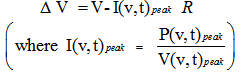 | (1) |
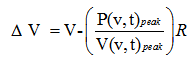 | (2) |
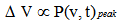 | (3) |
Where Switching, short circuit and glitch components of P(v,t)peak can be expressed as: | (4) |
Considering “m” logic gates contributing to peak power: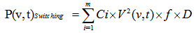 | (5) |
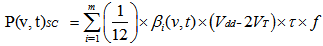 | (6) |
Where βi is the gain factor of the gate, τ is raise or fall time of the input signal, VT is threshold voltage, D is the activity factor, Ci load capacitance of the gate and f represents frequency. Glitch detection and glitch power calculation can be done by using power analysis results[17], where transmitted glitch can be defined as the pulse whose pulse width (PW) meets the following criteria: 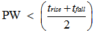 | (7) |
If the PW of the glitch doesn’t meet the criteria in above equation, then the signal does not reach the full voltage levels. The pulse width is determined from the VCD file and compared with the sum of the rise and fall transition times obtained from static timing analysis. Suppose that a gate G with inertial delay is dj(G) has “n” fanins in1,in2,…,inn and the arrival times of each fanin nodes are ta(inl),ta(in2), ...,ta(inn) respectively. WhenMax(ta(in1),ta(in2),…,ta(inm))-Min(ta(in1),ta(in2),..,ta(inm))> dj(G), glitches on the fanout node of G can be generated depending on input signals. Let's further suppose that the PW of glitches at fanin nodes are pw(in1),pw(in2),…,pw(inn-1) respectively. These glitches on fanin nodes can only be propagated through gate G if Max(pw(in1),pw(in2),…,pw(inn)) > dj(G). Hence a constant called glitch ratio (0 < GR < 1) is used to model the glitch power. The dynamic power (PNG) of the gate when there is no glitch is scaled with glitch ratio (GR) to estimate glitch power.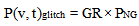 | (8) |
Where 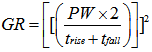 Hence we can conclude that:
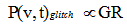 | (9) |
 | (10) |
 | (11) |
Now considering “q” number of gates (q < m and qj ⊂ mi) which are contributing to peak power. The glitch power can be expressed as: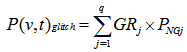 | (12) |
Reducing P(v,t)glitch is the subject of this work. For this we are using variable input delay method[7] which involves insertion of permanently on transmission gate at the input of logic gates to reduce differing delay at logic gate inputs. This intern will reduces glitch width and hence dynamic power. Consider the two input NAND gate shown in Fig 2. Suppose, the delay of path 1 to 3 is d1→3 and that of 2 to 3 is d2→3. The intrinsic inertial delay d3 of node 3 is independent of the input causing the output to change. It depends upon the total capacitance of node 3 and the resistance of ON transistors within the gate. Now the differential delay caused due to earliest arrival time of path 1 to 3 can be compensated by inserting transmission gate which consists of parallel connection of NMOS and PMOS. The transmission gate will pass logic 0 and 1 respectively without effecting voltage level of the signal. The effective resistance Reff of CMOS transmission gate is given by combined both transistors connected in parallel: 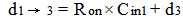 | (13) |
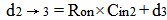 | (14) |
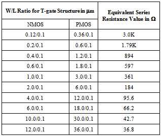
Where Cin1 and Cin2 are the input capacitances seen at the inputs of the gate and Ron is the series resistance of the ON transistors in the previous stage. The delay of the transmission gate due to Reff along with Ron for charging Cin1 is given by (Ron + Reff) ×Cin1. The effective resistance Reff can be increased by altering the (W/L) ratio of the transistors. We prepared a lookup table (LUT) using Synopsys SAED 90nm PDK for various Reff values by changing (W/L) ratio’s as shown in Table-1. Cin1 values and arrival times can be obtained by static timing analysis results and Reff can be computed. The proposed physical implementation flow is shown in Fig 3. From equation 1, 3, 9, 10, 11 & 14 we can conclude that the dynamic IR drop can effectively minimized by selective glitch reduction method using proposed flow.
5. Experimental Results
The proposed approach needs pre characterization of resistance cell created using pass gate. Resistance cell creation is done using Synopsys SAED 90nm PDKs[18]. HSPICE® is used to measure the effective resistance values of this pass gate structure and Look-up Tables (LUT) prepared as shown in in Table-1. Composite Current Source (CCS) Models for timing and power models are generated using Liberty-NCX® and standard cells layout for different dimensions of pass gate structure are created using Custom Designer®.Table 1. LUTs for Reff Prepared using Synopsys SAED 90nm PDK
 |
| |
|
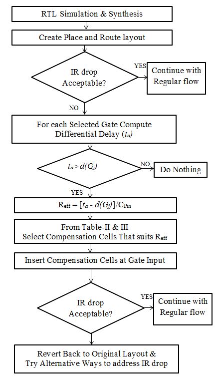 | Figure 3. Flow diagram for Proposed Methodology |
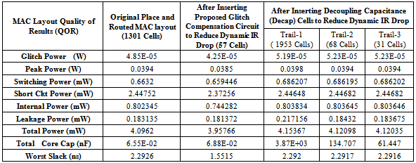
Table 2. MAC Layout Quality Metrics Compared With Proposed and Dcap Insertion Method
 |
| |
|
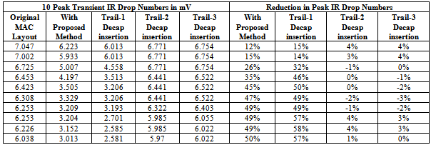
Table 3. MAC Layout Peak IR Drop Reduction Numbers with Proposed and Decap Insertion Method
 |
| |
|
Multiply-Accumulate (MAC) architecture with 16X16 multiplier and 32 bit accumulator word length is taken to corroborate the proposed methodology. MAC layout was implemented using SAED 90nm libraries. Design Compiler® is the tool used for carrying out synthesis. IC Compiler® is used for Floorplan, placement and routing. VCS-MX® is used for gate level simulation with 120 test vectors to generate Value Change Dump (VCD) switching activity file. Prime Rail® is used for doing dynamic IR drop analysis and Decap insertion. Decap insertion was done on place and routed MAC layout in three different trails to have the balance between total designs coupling capacitance versus design leakage. After implementing the proposed flow in original place and routed MAC layout the Quality of Results (QOR) are tabulated in Table-2. The reduction in transient peak IR drop numbers on MAC layout using proposed method and Decap insertion methods are compared and tabulated in Table-3. The results shows 12% to 50% reduction in top 10 peak IR drop numbers with just 12% glitch power reduction in selected combinational cells using proposed technique. The Decap insertion with optimal design leakage in Trail-2 and Trail-3 could only achieve 4% reduction in peak IR drop. The proposed flow will ensure that no new timing violations will be created via glitch compensation cells insertion. The key observation form Table-3 is that there is no increase in design leakage with proposed method whereas with Decap insertion method in Trail-1 the leakage power is increased by 20%. With the proposed method 3% decrease in total designs power is observed due to 12% glitch reduction. Fig 4 shows dynamic IR drop maps from IC Compiler® tool.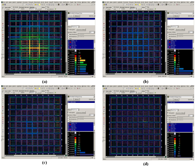 | Figure 4. Dynamic IR Drop Maps of MAC layout: (a) Original Place and Routed Layout (b) With Proposed Glitch Reduction Method (c) With Trail-2 Decap Insertion (d) With Tail-1 Decap Insertion |
6. Conclusions
By adopting the proposed selective glitch reduction technique the peak dynamic IR drop can be kept within allowable limits. The experimental results show that proposed technique it is more effective when compared to traditional Decap cell insertion technique with minimum compensation cells. The proposed flow can be seamlessly integrated into existing physical design flows.
References
| [1] | D.Brad and C.Vishweshwaraiah, “Inaccuracies in power estimation during logic synthesis,” proc. ICCAD, pp.388-394,1996. |
| [2] | L. Wang, M. Olbrich, E. Barke, T.Buchner, M. Buhler and P. Panitz, “A Gate Sizing Method for Glitch Power Reduction”, in SOCC IEEE Intl Conf, Sep 2011,pp. 24-29. |
| [3] | Hyungwoo Lee, Hakgun Shin, Juho Kim, “Glitch Elimination by Gate Freezing, Gate Sizing and Buffer Insertion for Low Power Optimization Circuit”, 30th annual conference of IEEE Industrial Electronics Society, Nov 2004, pp 2126-2131. |
| [4] | Vasantha Kumar.B.V.P, Murthy Sharma, K. Lal Kishore, Vivekanand. M, K. Murthy Raju and S. Divya Swetha. “A Physical Design Flow to Eliminate Glitch Power in Digital CMOs circuits”, World Congress On Information and communication Technologies (WICT20011), Mumbai, India, Dec 2011, pp. 639-644. |
| [5] | Vasantha Kumar.B.V.P, N.S.Murthy Sharma, K. Lal Kishore and A. Rajakumari, “Variable Input Delay CMOS logic for Dynamic IR Drop Reduction”, IEEE Asia-Pacific Conference on Postgraduate Research in Microelectronics & Electronics (PrimeAsia 2012), Hyderbad, Dec 2012, pp 79-84 |
| [6] | N. H. E.Weste and D. Harris, CMOS VLSI Design: A Circuits and Systems Perspective, 3 E. Boston, MA: Pearson Addison-Wesley, 2005. |
| [7] | T.Raja, V.D.Agarwal “Variable input delay CMOS logic for low power design”, IEEE Trans. Circuits syst.,vol.-17,no.10,October 2009. |
| [8] | K. Roy and S. C. Prasad, Low-Power CMOS VLSI Circuit Design. New York: Wiley, 2000. |
| [9] | V. D. Agrawal, “Low power design by hazard filtering,” in Proc. 10th Int. Conf. VLSI Des., Jan. 1997, pp. 193–197. |
| [10] | M. Berkelaar and E. T. A. F. Jacobs, “Gate sizing using a statistical delay model,” in Proc. Des. Autom. Test Eur. Conf., Paris, France, Mar. 2000, pp. 283–290. |
| [11] | V. Sundararajan, S. Sapatnekar, and K. Parhi, “Fast and exact transistor sizing based on iterative relaxation,” IEEE Trans. Comput.-Aided Des. Circuits Syst., vol. 21, no. 5, pp. 568–581, May 2002. |
| [12] | T. Raja, “A reduced constraint set linear program for low-power design of digital circuits,”M.S. thesis, Dept. ECE, Rutgers Univ., Piscataway, NJ, 2002. |
| [13] | T. Raja, V. D. Agrawal, and M. L. Bushnell, “Minimum dynamic power CMOS circuit design by a reduced constraint set linear program,” in Proc. 16th Int. Conf. VLSI Des., Jan. 2003, pp. 527–532. |
| [14] | R. Fourer, D. M. Gay, and B. M. Kernighan, AMPL:A Modeling Language for Mathematical Programming. South San Francisco, California: The Scientific Press, 1993. |
| [15] | David Stringfellow, John Pedicone, “Decoupling Capacitance Estimation, Implementation and verification: A Practical Approach for Deep Submicron SoCs”, proc. SNUG San Jose 2007. |
| [16] | Bozorgzadeh, B, Afzali-Kusha, A, “Novel MOS Decoupling Capacitor Optimization Technique for Nanotechnologies.” in 22nd Int. Conf. VLSI Des., Jan. 2009, pp. 175-180. |
| [17] | “Time Based Power Analysis”, Dec 2012, https://solvnet.synopsys.com/dow_retrieve/H-2012.12/ptpx/ptpx_6.html, Synopsys, Inc. |
| [18] | Goldman R., Bartleson K., Wood T., Kranen K., Cao C., Melikyan V., Markosyan G., "Synopsys' open educational design kit: capabilities, deployment and future", IEEE International Conference on Microelectronic Systems Education, 2009, pp. 20-24. |
 Abstract
 Reference
 Full-Text PDF
 Full-text HTML