P. Shravya Reddy1, Ramesh Vaddi2
1Department of Electronics and Communication Engineering, Padmasri Dr. B.V. Raju Institute of Technology, Hyderabad, India
2Department of Computer Science and Engineering, The Pennsylvania State University, University Park, PA 16802, USA
Correspondence to: Ramesh Vaddi, Department of Computer Science and Engineering, The Pennsylvania State University, University Park, PA 16802, USA.
| Email: |  |
Copyright © 2012 Scientific & Academic Publishing. All Rights Reserved.
Abstract
Operation of standard 6T static random access memory (SRAM) cells at sub or near-threshold voltages is unfeasible, predominantly due to degraded static noise margins (SNM) and poor robustness. In this paper, we analyze performance comparison of various alternative subthreshold SRAM bit cell topologies such as 8T, 9T and 10T for energy efficient and robust design at 45nm technology node. Co-design of subthreshold SRAM topologies with the different array architectures having asymmetric row/column sizes has also been explored for voltages down to 350mV for energy efficiency. 8T and 10T subthreshold SRAM cells along with the memory array architecture having lesser number of columns than rows is a better design choice in terms of having ultra-low cell leakage power, energy efficient and robust to PVT variations.
Keywords:
Alternative SRAM bit cells, Circuit/Architecture Co-design, Energy efficiency, Nano scale, Subthreshold, Ultra low power
Cite this paper: P. Shravya Reddy, Ramesh Vaddi, Alternative Bit-cell Topologies with Architecture Co-Design for Energy Efficient Nano Scale SRAM, Microelectronics and Solid State Electronics , Vol. 2 No. A, 2013, pp. 22-26. doi: 10.5923/s.msse.201302.03.
1. Introduction
The demand for ultra-low power or in strict sense energy efficient static random-access memory (SRAM) design has increased with the large use of SRAMs in system on-chip and high-performance VLSI circuits. The low-power requirement has often been met by compromising SRAM performance through the adoption of slower performing transistors with low leakage, and supply voltage scaling. As with most digital systems, embedded SRAMs play key role in energy-constrained applications such as biomedical, wireless sensor networks and mobile multimedia. They pose the most critical limitation to the total power, performance, and chip area. This can be demonstrated from three state-of-the-art examples[Figure 1] intended for increasingly low-power applications: the Intel Core 2 processor targeting mobile computing[1] (SRAM occupying ~ 20% of total power), the ARM1176JZ processor targeting hand-held computing[2] (~ 40% of total power), and the custom MSP430 microcontroller targeting remote wireless sensor and implantable biomedical computing[3] (~70% of total power).It has been demonstrated by several people that by operating circuits in the subthreshold region, circuits consume minimum energy per operation[4],[5]. Process variations limit the circuit operation in the subthreshold region, particularly the memories[6],[7]. Adaptive circuit techniques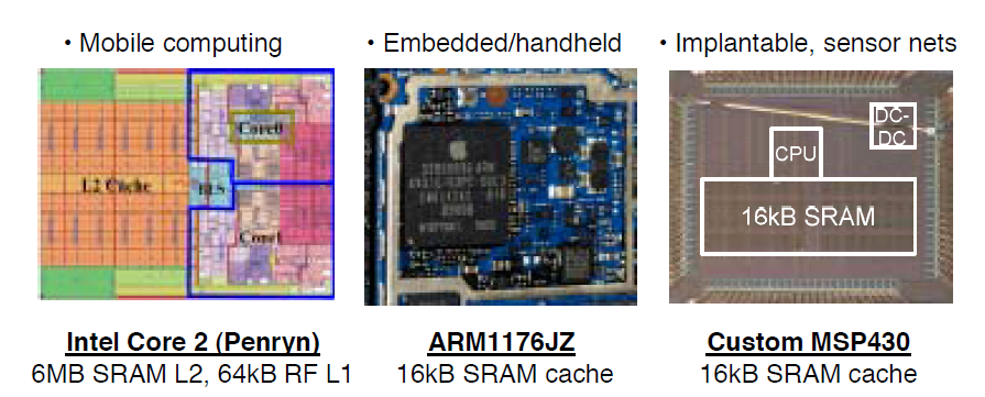 | Figure 1. Demonstration of ultra low power SRAM significance from three state-of-the-art examples targeting energy constrained applications[1-3],[14] |
such as source biasing, and dynamic have been proposed to improve the process variation tolerance[8]. Different types of alternative SRAM bitcells have been proposed to improve the memory failure probability at a given supply voltage[9]-[13]. 6T and 7T bitcells utilize differential read operation while 5T, 8T, and 10T bitcells employ the single-ended reading scheme. The 8T and 10T cells use an extra sensing circuit for reading the cell contents, achieving improved read stability[9]. J. P. Kulkarni,et al, in[9] propose a schmitt trigger based differential 10-transistor SRAM bitcell suitable for subthreshold operation and achieves 1.56 higher read static noise margin (SNM) compared to the conventional 6T cell at VDD=0.4V. In[10], the authors propose a novel 7T SRAM cell that only depends on one of the bit lines during a write operation and reduce the write power consumption by 49%. A 5.61 pJ, 16 kb 9T SRAM has been implemented in 65nm CMOS technology[11] with a proposed single-ended equalized bitline scheme to improve both read bitline voltage swing and sensing timing window. In[13], the authors propose a 10 T bitcell to solve the read SNM problem, write problem, and bitline integration limitations for sub-threshold operation.Although, many have proposed and explored various alternative SRAM bit cells for low voltage operation (at various older technology nodes), but not many have done a thorough comparative study of such cells at nano scale with architectural co-design for robust and energy efficient subthreshold SRAM design. In this paper, to the best of our knowledge, an extensive comparative analysis of subthreshold alternative bit cells such as 6T, 8T, 9T and 10T at 45nm technology node with architectural co-design approach for energy efficiency is done for the first time. The rest of the paper is organized as follows. Section 2 presents theoretical background of various subthreshold alternative bit cells. Performance comparisons of the various subthreshold alternative SRAM bit cells with PVT variations and Bit-cell co-design with SRAM architectures for energy efficiency has been described in section 3. Finally, conclusions are offered in Section 4.
2. Theoretical Background and Implementation Details of Subthreshold Alternative Bit-cell Topologies
This section summarize the theoretical explanation behind the operation of various subthreshold alternative bitcells such as 6T, 8T, 9T, and 10T.
2.1. 6T Subthreshold SRAM Cell
Implementation of subthreshold (VDD=350mv, Vth=450mv) 6T SRAM cell is shown in Figure 2. During the write operation, word line (WL) is raised and the BLs are forced to either VDD or GND (depending on the data), overpowering the contents of the memory cell . During the read operation, the WL voltage is raised, and the memory cell discharges either BL (bit line true) or BLB (bit line complement), depending on the stored data on nodes Q and QB. A sense amplifier converts the differential signal to a logic-level output. Then, at the end of the read cycle, the BL returns to the positive supply rail. During hold, WL is held low and the BLs are left floating or driven to VDD. The 6T SRAM cells fails its operation at subthreshold voltages.
2.2. 8T Subthreshold SRAM Cell
A dual-port cell (8T-cell) is created by adding two additional transistors (Figure 2); the read can be entirely decoupled from the write operation in an 8T cell by sensing the data through a separate read stack controlled by a separate read word lines (RWL).The remaining 6T portion of the cell is optimized for write, resulting in an overall lower Vmin. Separation of data retention element and data output element means that there will be no correlation between the read SNM Cell and I Cell. Thus, an 8TSRAM design[12] contains a write assist in which a horizontally routed VDD line is collapsed.
2.3. 9T Subthreshold SRAM Cell
Implementation of the 9T SRAM cell is shown in Figure 2[11]. It has a dedicated read port consisting of 3 NMOS transistors (M7, M8, and M9). Compared to the 8T SRAM cell, M9 is added for equalizing the read bitline leakage in unselected rows and providing a pull-up current path in a selected row to improve bitline sensing margin in case of reading ‘1’. During read (RWL=RVDD=’1’ and /SEL=’0’), the pre-charged read bitline (RBL) is conditionally discharged depending on ‘Q’ and ‘QB’. When reading data ‘1’ (Q=’1’), a pull-up path is formed from RWL to RBL through M9, which is different from the conventional 8T SRAM cell where both cell read current and bitline leakage current pull down RBL. The pull-up path slows down RBL discharging speed of data ‘1’ and improves RBL sensing margin. In standby modes, RVDD and /SEL are held to VDD to save the leakage current in the read port. The write operation of the proposed SRAM cell is the same as the conventional 8TSRAM.
2.4. 10T Subthreshold SRAM Cell
Figure 2 shows the implementation of 10T subthreshold SRAM bit cell[13]. The Write access to the bit cell occurs through the write access transistors, M5 and M6, Transistors from the write Bit-lines, WBLT and WBLC. Transistors M8 through M10 implement a buffer used for reading. Read access is single-ended and occurs on a separate bit-line, RBL, which is pre charged to prior to read access. The word-line for read also is distinct from the write word-line. One key Advantage to separating the read and write word-lines and bit lines is that a memory using this bit cell can have distinct read and write ports. 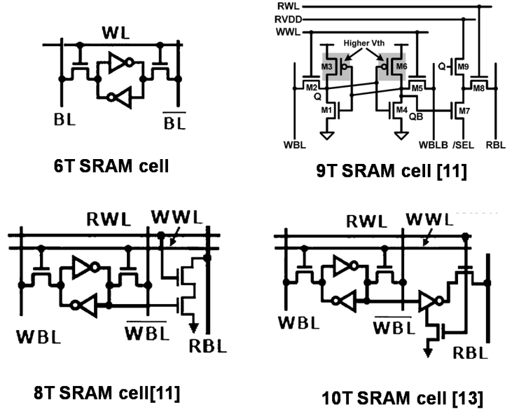 | Figure 2. Schematic of Subthreshold Alternative Bit cell Topologies |
3. Performance Analysis of Subthreshold Alternative Bit Cells with SRAM Architectural Co-Design
This section resents the performance analysis of subthreshold alternative bitcells such as 6T, 8T, 9T, and 10T with PVT variations. The simulations are carried out in Cadence Virtuoso[15] using 45nm technology. Table 1 summarizes the performance comparison of various subthreshold SRAM bit cells. It can be observed that, 8Tcell has 6 % lower bit line leakage compared to the 6T cell, whereas 9T SRAM cell has 1-2% lower leakage, and 10T cell has 16-20% lower bit line leakage. Figure 4 and 5 depict the comparison of leakage current and power variations of subthreshold alternative bit cells with temperature. It can be observed that 10T cell has the worst robustness, followed by 9T cell. 8T SRAM cell has the best robustness performance. 8T cell has almost 50% lower variation to temperature variations in comparison to 6T SRAM cell. Table 2 summarize the comparative study of robustness to temperature (% variation of leakage) of subthreshold alternative bit cells and it can be observed that 8T cell has the lowest variations.Fig. 5 and Fig. 6 show the comparison of read/write current and power variations of subthreshold alternative bit cells with supply voltage fluctuations. It can be observed that 9T and 10T SRAM cells have almost the similar robustness and worse in comparison to 8T SRAM cell having the best performance in terms of robustness (for a 100mv change in Vdd). Table 3 summarize the same and shows that 8T cell has the best robustness to Vdd variations in comparison to other alternative subthreshold SRAM bit cells.| Table 1. Read/Write current/power comparison of subthreshold alternative bit cells |
| | Bit celltopology | Bitline Read/Write Current (nA) | % lower in comparison with 6T | Bitline Read/Write power (nW) | % lower in comparison with 6T | | 6T SRAM | 2.23 | -- | 0.89 | -- | | 8T SRAM | 2.1 | 8.7 | 0.83 | 6.7 | | 9T SRAM | 2.20 | 0.5 | 0.88 | 1.1 | | 10T SRAM | 1.86 | 16.6 | 0.75 | 15.7 |
|
|
| Table 2. Comparative study of robustness to temperature variations of subthreshold alternative bit cells |
| | Bit cell topology | % variation of leakage current (for 10oC change) | comparisonwith 6T | % variation of leakage power(for 10oC change) | comparison with 6T | | 6T SRAM | 7 | -- | 7 | -- | | 8T SRAM | 1.5 | 78.2% lower | 0.1 | 54.2% lower | | 9T SRAM | 9 | 28.5% higher | 9 | 31% higher | | 10T SRAM | 2 | 77.7 %lower | 1.2 | 57.4% higher |
|
|
| Table 3. Comparative study of robustness to Vdd variations of subthreshold alternative bit cells |
| | Bit cell topology | % variation of read/write current (for 100 mv change) | % variation of read/write power (for 100 mv change) | | 8T SRAM | 32 | 32 | | 9T SRAM | 41 | 65 | | 10T SRAM | 48 | 77 |
|
|
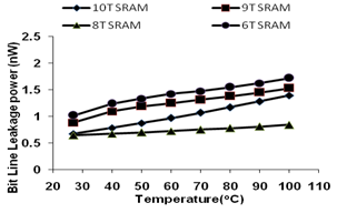 | Figure 4. Bit Line leakage power variation of alternative subthreshold SRAM bit cells with temperature |
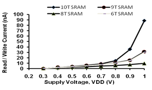 | Figure 5. Read/Write current variation of alternative subthreshold SRAM bit cells with supply voltage |
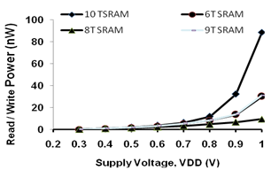 | Figure 6. Read/Write current power variation of alternative subthreshold SRAM bit cells with supply voltage |
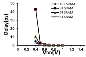 | Figure 7. Read/Write delay of alternative subthreshold SRAM bit cells with supply voltage |
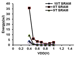 | Figure 8. Read/Write energy of alternative subthreshold SRAM bit cells with supply voltage |
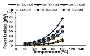
Figure 7 present read/write delay variation of subthreshold SRAM bit cells with supply voltage scaling. It can be observed that delays are smaller for 6T and 10T cells. The read/write delay of the 10T cell is of 85% less compared to the 8T cell. From Figure 8 it can be summarized that, 10TSRAM cell is more energy efficient in comparison to the other subthreshold alternative bitcells. Finally, an architectural co-design approach with subthreshold alternative bit cells has been performed. Subthreshold SRAM of 1Kb size is designed with different bit cells and for different arrays sizes (i.e, same array size but with different row/column sizes, 32X32 array, 64X16, 128X8). Figure 9 shows the array size variations on 8T SRAM leakage power with temperature variations and it is observed that the arrays with the less number of columns than rows will have a better reduction in the leakage power when compared to the array having high column number or symmetric case. That means, 128X8 array is having less leakage power than the arrays having the higher columns i.e. 32x32, 64X16 SRAM arrays. The 8T SRAM array with 128x8 is having 60% less power leakage than the 6T RAM array with 128X8 array size. Also, 8T cell with an array size of 64X16 has 40% less leakage to 32X32 array size and 65% of more leakage compared to array of 128X8. Figure 10 compares the 8T and 10T SRAM array performance with architecture co-design for temperature variations. Overall, 10T cell topology with 128x8 has smaller leakage power than other configurations of 10T and 8T has more leakage power than 10T with either configurations.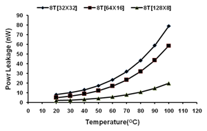 | Figure 9. Bit Line leakage power variation of 8T subthreshold SRAM bit cell for temperature with architecture co-design |
 | Figure 10. Leakage power comparison of 8T and 10T SRAM arrays with architecture co-design |
4. Conclusions
Performance comparison of various subthreshold alternative bit cells such as 8T, 9T, 10T with the conventional 6T SRAM cell is performed. It has been shown that in terms of leakage power reduction and energy, 10T SRAM cell has the best performance in comparison to 8T and 9T cells and almost 78% lower leakage power than 6T cell. In terms of robustness to variation in temperature (for 10oC change) and variation in supply voltage (for a 100mv change), the 8T SRAM cell has the best performance. An architectural co-design approach of above alternative SRAM bit cells with different row/column sizes was also performed in the end for the same array size. The 10T and 8 T SRAM arrays with small columns than row number have better energy and low leakage characteristics. With further specific architectural and circuit techniques, 8T and 10T SRAM cell topologies can provide energy efficient and robust subthreshold SRAM design solutions for energy constrained applications.
References
| [1] | V. George, S. Jahagirdar, C. Tong, K. Smits, S. Damaraju, S. Siers, V. Naydenov, T. Khondker, S.Sarkar, and P. Singh, “Penryn: 45-nm next generation intel core 2 processor,” in Proc. IEEE Asian Solid-State Circuits Conference, Nov. 2007, pp. 14–17. |
| [2] | ARM,“Arm1176jz(f)-s,”http: // www. arm.com/ products/ CPUs/ ARM1176. html. |
| [3] | J. Kwong, Y. Ramadass, N. Verma, M. Koesler, K. Huber, H. Moormann, and A. Chandrakasan, “A 65nm sub-vt microcontroller with integrated SRAM and switch-capacitor DC-DC converter,” in IEEE Int. Solid-State Circuits Conf. Dig. Tech. Papers, Feb. 2008, pp. 318–319. |
| [4] | R. vaddi, S. Dasgupta, R. P. Agarwal “Device and Circuit Design Challenges in the Digital Subthreshold Region for Ultra- Low Power Applications”, VLSI Design Journal, Hindawi publishing corporation, Vol. 2009, Article No. 1 ,Jan.2009. |
| [5] | J. Kwong et al., ‘‘A 65 nm Sub-Vt Microcontroller with Integrated SRAM and Switched Capacitor DC-DC Converter,’’ IEEE J. Solid-State Circuits, vol. 44, no. 1, pp. 115-126, 2009. |
| [6] | A. Bhavnagarwala, X. Tang, and J. Meindl, “The impact of intrinsic device fluctuations onCMOS SRAMcell stability,” IEEE J. Solid-State Circuits, vol. 36, no. 4, pp. 658–665, Apr. 2001. |
| [7] | S. Mukhopadhyay, H. Mahmoodi, and K. Roy, “Modeling of failure probability and statistical design of SRAMarray for yield enhancement in nanoscaled CMOS,” IEEE Trans. Comput. Aided Des., vol. 24, no.12, pp. 1859–1880, Dec. 2005. |
| [8] | H. Kawaguchi, Y. Itaka, and T. Sakurai, “Dynamic leakage cutoff scheme for low-voltage SRAMs,” in VLSI Circuits Symp. Dig., Jun.1998, pp. 140–141. |
| [9] | J. P. Kulkarni, K. Kim, and K. Roy, BA 160mV robust schmitt trigger based subthreshold SRAM, IEEE J. Solid-State Circuits, vol. 42,no. 10, pp. 2303–2313, Oct. 2007. |
| [10] | R. Aly, M. Faisal, and A. Bayoumi, “Novel 7T SRAM cell for low power cache design,” in Proc. IEEE SOC Conf., 2005, pp. 171–174. |
| [11] | Q. Li, B. Wang, and T. Kim, "A 5.61 pJ, 16 kb 9T SRAM with Single-ended Equalized Bitlines and Fast Local Write-back for Cell Stability Improvement", IEEE European Solid-State Device Research Conference, pp. 201-204, Sept. 2012. |
| [12] | L. Chang, D. Fried, J. Hergenrother, J. Sleight, R. Dennard, R. R. Montoye, L. Sekaric, S. McNab, W. Topol, C. Adams, K. Guarini, and W. Haensch, “Stable SRAM cell design for the 32 nm node and beyond,” in Symp. VLSI Technology Dig., 2005, pp. 128–129. |
| [13] | B. H. Calhoun and A. P. Chandrakasan, “A 256 kb subthreshold SRAM in 65 nm CMOS,” in IEEE Int. Solid-State Circuits Conf. (ISSCC) Dig. Tech. Papers, 2006, pp. 628–629. |
| [14] | Naveen Verma, PhD. Thesis, “Ultra-Low-Power SRAM Design In High Variability Advanced CMOS”, department of Computer Science and Electrical Engineering, mIT, June 2009. |
| [15] | Cadence® Virtuoso® Spectre® Circuit Simulator, 2009. |
 Abstract
 Reference
 Full-Text PDF
 Full-text HTML