Jitendra Kanungo, S. Dasgupta
Microelectronics & VLSI Group, Department of Electronics and Computer Engineering. Indian Institute of Technology, Roorkee-247667 , India
Correspondence to: S. Dasgupta, Microelectronics & VLSI Group, Department of Electronics and Computer Engineering. Indian Institute of Technology, Roorkee-247667 , India.
| Email: |  |
Copyright © 2012 Scientific & Academic Publishing. All Rights Reserved.
Abstract
Extensive research is carried-out worldwide to design energy-efficient adiabatic circuits for such biomedical and space applications where conventional energy is limited and speed is not critical. In this paper a new single phase adiabatic or energy recovery logic is proposed and extensively analyzed the energy performance with technology scaling. We present a comparative study among proposed logic gate, reported single phase adiabatic logic gates and static CMOS logic gate at different technology nodes. For this purpose the 4-stage inverter chains of proposed and reported single phase adiabatic logic families were simulated at 180 nm, 90 nm and 45 nm technology nodes and results show that the energy recovery or adiabatic logic circuits can be used for nanoscale ultra low power application.
Keywords:
Adiabatic Logic, Energy Recovery, Single Phase Energy Recovery Logic
Cite this paper: Jitendra Kanungo, S. Dasgupta, Single Phase Energy Recovery Logic and Conventional CMOS Logic: A Comparative Analysis, Microelectronics and Solid State Electronics , Vol. 2 No. A, 2013, pp. 16-21. doi: 10.5923/s.msse.201302.02.
1. Introduction
The energy recovery logic is the best candidate for achieving ultra low power digital applications which significantly reduces the energy consumption and ultimately the heat generated. These circuits recover the un-dissipated energy related to charges stored in the device parasitic capacitance and resistance and recycle though an efficient resonant power supply[1],[2]. In the last few years, multi phase and single phase energy recovery logics[3]-[13] have been suggested but single phase energy recovery logic circuits are more attractive for their reasonable speed and small area in ultra low power integrated circuit design. The motivation behind this research work is to explore the energy efficiency and functionality of new single phase energy recovery logic with progressive CMOS technology scaling. In this paper, the work is focused on the study of energy efficiency of proposed logic and other reported single phase adiabatic logic and their comparison at various nanoscale CMOS technology. Proposed Single Phase Adiabatic Logic (SPAL)[14] uses a single phase sinusoidal power supply source, providing lower energy dissipation with simplified clocking management. SPAL substantially decreases the transistor count and easily resemble to static logic. To prove the functionality of efficient proposed logic, single inverter and four stage inverter chains have been implemented at 45 nm, 90 nm, 180 nm technology nodes[15]. Results are extensively compared and analyzed with Clocked Adiabatic Logic (CAL)[9],[10], Source Coupled Adiabatic Logic-Diode connected (SCAL-D)[11]-[13] and conventional CMOS design. Results show the importance of energy recovery logic in CMOS nanotechnology era.Paper is organized as follows: Proposed logic and reported logics are described in Section 2. Results and discussion are carried out in Section 3 and finally, concluding remarks are presented in Section 4.
2. Proposed and Reported Adiabatic Logic Circuits
2.1. Proposed Adiabatic Logic
Fig. 1 shows the SPAL inverter circuit[14], that comprises a pair of MOS diodes (P1-P2 and N1-N2), and a functional block (MP and MN). The SPAL uses a single phase power clock (Φ) that operates SPAL gate for the purpose of charging and discharging. The SPAL circuit works as follows[14]:Charging Process: - Let, power clock (Φ) ramps up to HIGH, circuit input node ‘in’ and output node ‘out’ are LOW. This makes a conducting path: Φ - MOS diode - MP - out. Hence, circuit output node ‘out’ follows clock supply Φ and swings to HIGH. When ‘out’ reaches Φmax - |Vtp|, the MOS diode cuts-off and ‘out’ remains at HIGH. The LOW input keeps MN in OFF state that isolates the ‘out’ from supply Φ. In this way, ‘out’ remains unchanged. Discharging Process: - Let, power clock (Φ) ramps down to 0, and both circuit input node ‘in’ and output node ‘out’ are HIGH. This makes a conducting path: out - MN - MOS diode - Φ. Hence, ‘out’ follows Φ as it swings LOW. As a result, small amount of current flows toward the power supply Φ, that enables the recycling of energy stored in output capacitance C. When, the voltage at ‘out’ node reaches at Vtn the transistor MN is turned off and ‘out’ remains at LOW. The output logical state does not change unless the input changes. Hence, charging and discharging of output node depends upon input transition. Diodes composed by the parallel combinations of P1-P2 and N1-N2 reduce the effective resistance of charging and discharging path respectively.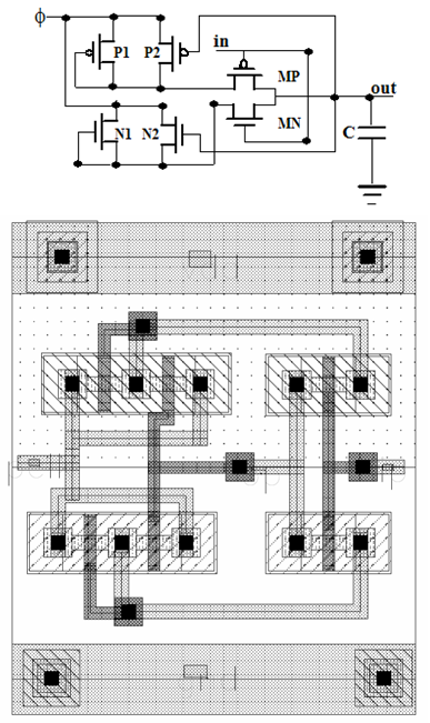 | Figure 1. SPAL inverter circuit[14] and its layout |
If a conventional CMOS inverter and the SPAL inverter are compared, then main differences are: SPAL uses a parallel combination of transistors with pull-up and pull-down networks to charge the output capacitance and it recycles the energy from charge stored in output node capacitance. Threshold voltage drop across pull up network and ON resistance results in the energy dissipation (EPUN) in the charging of output capacitance[14], it can be written as: | (1) |
Where C is the output capacitance, |Vtp| is threshold voltage of pull up device, RP,ON is the on-resistance of pull up device MP1, T is charging time of ‘out’ node capacitance, and VΦmax is maximum supply voltage. Similarly, energy consumption due to parallel combination of PMOS devices P1 and P2 in charging the ‘out’ node capacitance C would be: | (2) |
Req the resistance is due to parallel PMOS devices P1 and P2, it can be obtained from the conductance of device in their conducting mode: | (3) |
G1 and G2 are device conductance of P1 and P2 respectively and V is the net voltage across MOS diode. Thus, total energy consumption in charging path would be: | (4) |
The Discharging process dissipates almost same amount of energy.
2.2. Reported Adiabatic Logic Circuits
2.2.1. Clocked Adiabatic Logic (CAL)
The clocked adiabatic logic (CAL) inverter[9] is shown in Figure 2. Cross-coupled CMOS inverters, transistors P1, N1, P2 and N2 provide the latch function. CX signal controls transistor MN1 and MN2 that are in series with the logic trees represented by M3 and M4. CX enabled devices MN1 and MN2 allow operation with a single power clock (Φ). This auxiliary timing control clock signal CX, introduced, to realize an adiabatic logic function with a single power clock (Φ). Auxiliary clock CX enables the logic evaluation. For ‘in’ = 0, N4 and MN2 are on, causing ‘outb’ = 0 and P1 to be on, and thus allowing output ‘out’ to closely follow the power clock waveform. Next, when the auxiliary clock CX = 0 disables the logic evaluation. In CAL circuit transistors MN1 and MN2 does not work in adiabatic manner due to application of auxiliary clock CX.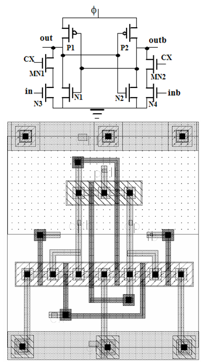 | Figure 2. CAL inverter/buffer circuit and its layout[9] |
For a large logic circuit, this results in undesired energy dissipation[9].
2.2.2. Source Coupled Adiabatic Logic–Diode Connected (SCAL-D)
The Source Coupled Adiabatic Logic with Diode connected transistors (SCAL-D)[12] is a partially adiabatic logic family that is clocked by a single-phase power clock. The basic structure of SCAL-D NMOS inverter is shown in Fig. 3. This NMOS buffer comprises a pair of cross-coupled transistors (N1 and N2), a pair of diode connected transistors (DN1 and DN2), a pair of current control switches (N3 and N4), two functional blocks (N5 and N6), and a current source (N7 and N8) biased by a constant voltage VBN and a sinusoidal power clock (Φ). Each SCAL-D NMOS gate goes through an evaluation and a discharge phase. During discharge, the energy stored in the output node (‘out’ or ‘outb’) is recovered through the pair of cross-coupled transistors (N1 and N2) and the pair of diode-connected transistors (DN1 and DN2). In this phase, Φ starts from HIGH and ramps down to LOW, pulling both of ‘out’ or ‘outb’ down toward the pre discharge voltage. This state change tracks the power-clock and, thus, recovers charge from the output nodes. Some amount of the charge is recovered through a device with a constant voltage drop. In the evaluation phase, Φ starts rising from LOW, turning N1 and N2 on along the way. When gate-to-source voltage of current source N7 exceeds Vtn, N7 turns on and raises the voltage at its drain end, while N3 and N4 are conducting. Therefore, assuming ‘in’ is HIGH and ‘inb’ is LOW, a path is created from ‘out’ to GND and ‘outb’ starts rising towards HIGH. 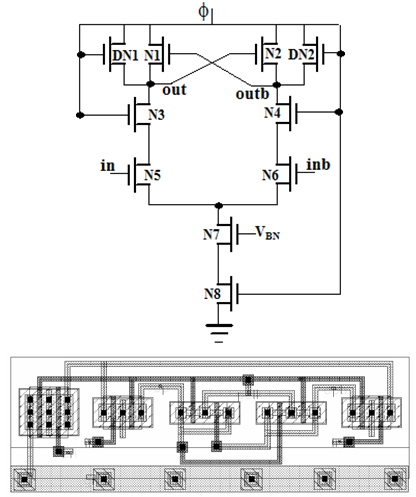 | Figure 3. SCAL-D NMOS inverter/buffer circuit and its layout[12] |
Cross-coupled latch functions as a sense-amplifier and boosts the voltage difference of two output nodes. However, initially a dissipative current is directed by the functional block, creating a small voltage imbalance between the outputs that can be controlled by the sizing of current source transistors.
3. Results and Discussion
The sinusoidal signal is an efficient clock signal. In this paper for all described adiabatic circuits, sinusoidal signal is applied as a single phase clock supply and a charge recovering device. An energy efficient clock generation technique that has been applied in the analysis is shown in Fig. 4[16]. The oscillation of RLC circuit is maintained by the transistor MN1. This large transistor is driven by buffer circuit of progressively sized inverters. The oscillation frequency of this clock generator is given by the formula: | (5) |
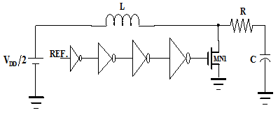 | Figure 4. The schematic of an energy recovery sinusoidal clock generator [16] |
The energy consumption for an individual adiabatic circuit is determined using the flowing equation: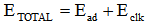 | (6) |
Where Ead is energy consumption due to adiabatic circuit and Eclk is energy consumption due to power clock generator. Since, the total energy consumption is strongly determined by the choice of the clock generation technique, therefore energy consumption of the clock generator is not included in the total energy consumption. During simulation it is observed that the adiabatic approach gives reduced energy consumption (3 to 6 fold) with respect to a logically equivalent static CMOS approach even though the power-clock generation loss has been considered. The power-clock signal distribution is the main issue in adiabatic circuit design. Since, the clock frequencies at which adiabatic circuits gives significant energy saving and constitute a competitive alternative approach to CMOS design are low, and then therefore power-clock transitions needs to be slow-down about to one quarter of the period of the waveform. Thus, the clock distribution issue is more relaxed than and not as critical as in traditional CMOS. In case of possible jitter or skew the correct functionality of the gates can be achieved if power-clock adjacent phases are perfectly synchronized to each other[17]. We designed the 4-stage inverter chains using SPAL, CAL (Fig. 2), SCAL-D (Fig. 3) and static CMOS logic[2] and simulated in the clock frequency range from 50 MHz to 500 MHz. Load capacitance of 3 fF is connected at the output node of each type of inverter. Peak-to-peak sinusoidal voltage supply of 0.8 V, 1 V and 1.8 V are applied at 45 nm, 90 nm and 180 nm technology nodes[15] respectively. The electrical simulations have been carried out through Cadence Spectre simulator. For each type of adiabatic logic the frequency of the input signal(s) is kept 6 times of clock frequency and energy consumption is measured against various clock frequencies for an input cycle. However, for fair comparison the input frequency in conventional CMOS circuit is kept equals to power clock frequency and measured the energy consumption for same amount of time. Fig. 5(a) shows the energy consumption versus clock frequency for 4 stage inverter chains at 45 nm. At 300 MHz clock frequency, proposed SPAL gives adiabatic gain (ratio of energy consumption of logically equivalent static CMOS logic and energy consumption of adiabatic logic) of 7.87 as compared to 5.91 of SCAL-D and 3.94 of CAL. Circuit operation at 500 MHz clock frequency the adiabatic gain of 6.82 for SPAL, 5.19 for SCAL-D and 3.41 for CAL have been obtained. In Fig. 5(b) the energy consumption versus clock frequency is shown for 90 nm technology node. The CAL and SCAL-D competes with SPAL at a clock frequency less than 200MHz but at higher frequency SPAL outperforms. Although, SPAL circuit shows the output swing dropped by a device threshold voltage and slower speed but it enables the better power/energy efficiency. Fig. 5(c) demonstrates the energy consumption of four inverter chains as a function of clock frequency at 180 nm technology node. At 300 MHz clock frequency, proposed SPAL shows adiabatic gain of 12.46 while, it is 5.92 and 2.53 for SCAL-D and CAL respectively. Similarly, at 500 MHz clock frequency adiabatic gain for SPAL is 7.30, 4.25 for SCAL-D and 1.62 for CAL. Thus, SPAL has better energy efficiency than CAL, SCAL-D and static CMOS counterpart.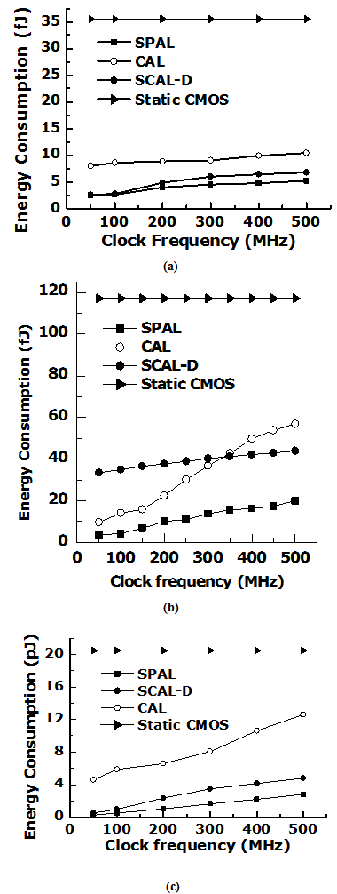 | Figure 5. Energy consumption versus clock frequency at (a) 45 nm (b) 90 nm and (c) 180 nm |
The results are summarized in Table 1 and further the energy performance of logic circuits with scaling technology have been drawn in Fig. 6. The adiabatic gain of each type of single phase adiabatic logic has been determined. It helps us to choose an efficient single phase adiabatic logic for a clock frequency range. At a clock frequency less than 200 MHz the SPAL shows higher adiabatic gain than SCAL-D and CAL. In fact, with increasing clock frequency associated transit time is decreased that ultimately limits energy saving. In clock frequency range from 50 MHz to 500 MHz the SCAL-D logic shows least variation in adiabatic gain. On the other hand, adiabatic gain of SPAL and CAL logics were affected by clock frequency and therefore large variation in their adiabatic gains can be seen.  | Figure 6. Adiabatic gain versus clock frequency at (a) 45 nm (b) 90 nm and (c) 180 nm |
Thus, we conclude that SPAL is limited by operating clock frequency and should be taken in to account during design. Delay analysis for SPAL, CAL and SCAL-D inverters is also carried for 3 fF load capacitance and clock frequency range from 50 MHz to 500 MHz. The results given in Table 2 show that CAL and SCAL-D adiabatic inverters are better in speed than SPAL. The transistor count for the described adiabatic inverter chains are presented in Table 3, SPAL approach is comparable to CAL and SCAL-D.| Table 1. Adiabatic gain versus clock frequency |
| | Node | Adiabatic Gain | | SPAL | CAL | SCAL-D | | Clock Frequency (MHz) | Clock Frequency (MHz) | Clock Frequency (MHz) | | 100 | 200 | 300 | 400 | 500 | 100 | 200 | 300 | 400 | 500 | 100 | 200 | 300 | 400 | 500 | | 45nm | 13.70 | 8.78 | 7.87 | 7.36 | 6.82 | 12.76 | 7.25 | 5.91 | 5.53 | 5.19 | 4.11 | 4.01 | 3.94 | 3.57 | 3.41 | | 90nm | 20.05 | 11.58 | 8.54 | 7.22 | 5.88 | 8.24 | 5.22 | 3.17 | 2.38 | 2.06 | 3.33 | 3.10 | 2.91 | 2.78 | 2.66 | | 180nm | 24.18 | 20.24 | 12.46 | 9.29 | 7.30 | 21.19 | 8.58 | 5.92 | 4.91 | 4.25 | 3.49 | 3.10 | 2.53 | 1.92 | 1.62 |
|
|
| Table 2. Comparison of delay for inverters |
| | Circuits | Delay (ns) | | 50 MHz | 100 MHz | 200 MHz | 300 MHz | 400 MHz | 500 MHz | | SPAL | 4.40 | 3.94 | 3.25 | 2.14 | 1.71 | 1.40 | | CAL | 4.79 | 3.41 | 1.93 | 1.78 | 0.91 | 0.76 | | SCAL-D | 4.26 | 3.01 | 2.67 | 2.11 | 1.62 | 1.46 |
|
|
| Table 3. Comparison of transistor count |
| | Circuits | No. of Transistors | | SPAL | CAL | SCAL-D | CMOS | | 4-inverter chain | 24 | 32 | 40 | 8 |
|
|
4. Conclusions
In this paper, we have shown that the energy recovery logic is a good candidate for achieving ultra low power nanoscale digital design. Since, selection of energy recovery power clock generator is a matter of circuit design and application. Therefore, we have obtained the results for an ideal sinusoidal power clock. But, we have also observed the results by applying an energy recovery sinusoidal power clock. At 500 MHz clock frequency significant energy saving has been achieved from proposed SPAL, reported CAL and SCAL-D designs respectively. Proposed logic is energy efficient at the cost of delay and presented work makes ease for any digital VLSI circuit engineer to adopt energy recovery logic or adiabatic logic among the other low power CMOS circuit techniques.
ACKNOWLEDGEMENTS
This research work is supported by the project “Special Manpower Development Programme for VLSI & related software – Phase II (SMDP-II)”, DIT, Govt. of India.
References
| [1] | Jitendra Kanungo and S.Dasgupta, “Study of Energy Efficiency of Single Phase Energy Recovery Logic with Progressive Technology” In proceeding of 15th VLSI Design And Test Symposium, 1-10 (2011). |
| [2] | Weste, N.H.E. and K. Eshraghian, “Principles of CMOS VLSI Design”. Addison-Wesley Reading USA, (1985). |
| [3] | A. Blotti, S. Di Pascoli, and R. Saletti, “A Comparison of Some Circuit Schemes for Semi-reversible Adiabatic Logic” International Journal of Electronics, 89, 147 (2002). |
| [4] | A. G. Dickinson and J. S. Denker, “Adiabatic dynamic logic” IEEE Journal of Solid-State Circuits, 30, 311 (1995). |
| [5] | Jan M. Rabaey, and Massoud Pedram, “Low Power Design Methodologies” Kluwer Academic Publishers USA, (2002). |
| [6] | J.S. Denker, “A Review of adiabatic Computing” In proceeding of the IEEE Symposium on Low Power Electronic, Digest of Technical Papers, 94 (1994). |
| [7] | Y. Ye and K. Roy, “Energy Recovery Circuits Using Reversible and Partially Reversible Logic” IEEE Transaction on Circuits and Systems-I, 43, 769 (1996). |
| [8] | S. G. Younis and T. F. Knight, “Asymptotically Zero Energy Split-level Charge Recovery Logic” In proceeding of the International Workshop on Low Power Design, 177 (1994). |
| [9] | D. Maksimovic, V. G. Oklobdzija, B. Nikolic, and K. W. Current, “Clocked CMOS Adiabatic Logic With Integrated Single Phase Power-clock Supply” IEEE Transaction on Very Large Scale Integration Systems, 8, 460 (2000). |
| [10] | C. Luo and J. Hu, “Single-phase adiabatic flip-flops and sequential circuits using improved CAL circuits” In pro ceeding of International Symposium on Low-Power Electronics Design, 97 (1999). |
| [11] | S. Kim and M.C. Papaefthymiou, “True single-phase adiabatic circuitry” IEEE Transaction on VLSI Systems, 9, 52 (2001). |
| [12] | S. Kim, C.H. Ziesler and M.C. Papaefthymiou, “A true single-phase energy recovery multiplier” IEEE Transaction on Very Large Scale Integration Systems Systems, 11, 194 (2003). |
| [13] | S. Kim and M.C. Papaefthymiou, Single-phase source-coupled adiabatic logic. In proceeding of IEEE conference on ASIC, 124 (2007). |
| [14] | Jitendra Kanungo and S.Dasgupta, “An Efficient Single-phase Adiabatic Logic and Its Application to Combinational and Sequential Logic” ASP Journal of Low Power Electronics, 7, 381(2011). |
| [15] | https://pdk.cadence.com/home.do |
| [16] | H. Mahmoodi, V. Tirumalashetty, M. Cooke and K. Roy, “Ultra low-power clocking scheme using energy recovery and clock gating, IEEE Transaction on Very Large Scale Integration Systems” 17, 33(2009). |
| [17] | A. Blooti and R. Saletti, Ultralow-power adiabatic circuit semi-custom design” IEEE Transaction on Very Large scale Integration Systems, 12, 1248 (2004). |
 Abstract
 Reference
 Full-Text PDF
 Full-text HTML