-
Paper Information
- Next Paper
- Paper Submission
-
Journal Information
- About This Journal
- Editorial Board
- Current Issue
- Archive
- Author Guidelines
- Contact Us
Microelectronics and Solid State Electronics
p-ISSN: 2324-643X e-ISSN: 2324-6456
2013; 2(A): 1-15
doi:10.5923/s.msse.201302.01
Device/Circuit/Architectural Techniques for Ultra-low Power FPGA Design
 Abstract
 Reference
 Full-Text PDF
 Full-text HTML
Pooran Singh, Santosh Kumar Vishvakarma
Nanoscale Devices and VLSI/ULSI Circuit & System Design Lab School of Engineering, Electrical Engineering Discipline, Indian Institute of Technology (IIT), Indore, MP, 145341, India
Correspondence to: Santosh Kumar Vishvakarma, Nanoscale Devices and VLSI/ULSI Circuit & System Design Lab School of Engineering, Electrical Engineering Discipline, Indian Institute of Technology (IIT), Indore, MP, 145341, India.
| Email: |  |
Copyright © 2012 Scientific & Academic Publishing. All Rights Reserved.
Field Programmable Gate Arrays (FPGAs) are widely used for implementation of digital system design due to their flexibility, low time-to-market, growing density and speed. But the Power consumption, especially leakage and dynamic power has become a major concern for semiconductor industries. FPGAs are less power-efficient than custom ASICs, due to the overhead required to provide programmability. Despite this, power has been largely ignored by the FPGA research community earlier, whose prime focus centred on improving FPGA speed and area-efficiency. But nowadays research extensively focuses on power too. Hence this paper demonstrates some of the most utilized and efficient techniques for Power optimization and reduction in FPGAs currently. After reviewing latest research work on power reduction in FPGA we examined that using Dual VT and fine-grained VDD static power reduces upto 64% and 95% respectively. Clock Gating reduces the power consumption by the factor 50% and also by using latest novel devices like Tunnel FET power can be reduced much lower than present.
Keywords: FPGA, Power Reduction, CAD, SRAM, Non-Classical MOS Devices
Cite this paper: Pooran Singh, Santosh Kumar Vishvakarma, Device/Circuit/Architectural Techniques for Ultra-low Power FPGA Design, Microelectronics and Solid State Electronics , Vol. 2 No. A, 2013, pp. 1-15. doi: 10.5923/s.msse.201302.01.
Article Outline
1. Introduction
- Field-Programmable Gate Arrays (FPGAs) are integrated circuits that can be programmed to implement any digital circuit. The main difference between FPGAs and conventional fixed logic implementations, such as Application Specific Integrated Circuits (ASICs), is that the designer/customer programs the FPGA on-site[1-3]. For fixed logic implementations, the designer must create a layout mask and send it to a foundry to be fabricated. Creating a layout is labour-intensive and requires expensive CAD tools and experienced engineers. Programmable switches controlled by configuration memory occupy a large area in the FPGA and add a significant amount of parasitic capacitance and resistance to the logic and routing resources. Because of this, FPGAs are approx 3 times slower, 20 times larger, and 12 times less power efficient compared to ASICs[4].Many studies have focused on reducing the speed and area overhead of FPGAs. Important advancements include cluster-based logic blocks[5], which improve speed by grouping the basic logic elements of the FPGA into clusters with faster local interconnect; embedded memories[6], which reduce the speed and area overhead for applications with storage requirements; and embedded ALUs[7], which reduce the speed and area overhead for applications that perform arithmetic operations. A significant number of studies have also focused on faster; more area efficient programmable routing resources[8]. As CMOS process technology scales down, the power density continues to increase due to higher chip operating frequencies, higher total interconnect capacitance per chip, and increasing leakage. Indeed, the International Technology Roadmap for Semiconductors has identified low-power design techniques as a critical technology need[9]. This paper is organized as follows. Section 2 describes the basic architecture of an FPGA; Section 3 summarizes the sources of power dissipation; Section 4 covers different power reduction techniques Finally, Section 5 summarizes the paper and proposes future work.
2. FPGA Architecture
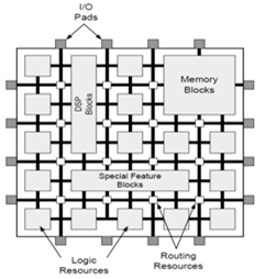
- A basic symmetric FPGA is shown in Fig.1. The FPGA architecture is very regular in structure[10, 11]. It is made up of two main components-Configuration logic blocks (CLBs) and routing resources. The logic blocks implement the functionality of the given circuit while the routing resources provide the connectivity for implementing the logic. The logic blocks have the flexibility to connect to the routing resources surrounding them. The logic blocks and the routing resources are configurable, so that they can be programmed to implement any logic. Though many types of architectures have been experimented with, the most popular one is the SRAM based architecture[10, 11]; the architecture connected with programmable logic interconnects shown in Fig.2.
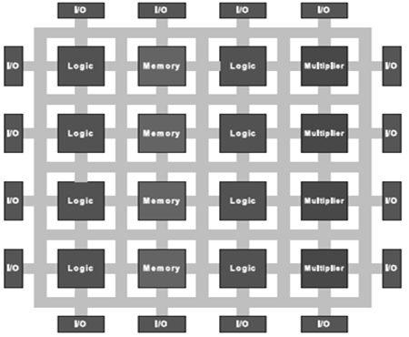 | Figure 1. A basic FPGA[10] |
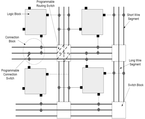 | Figure 2. FPGA basic architecture[11] |
2.1. Logic Block
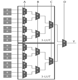
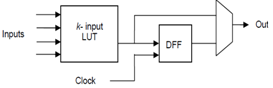
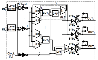
- The logic block of the SRAM based FPGA is LUT (look-up-table) based and composed of basic logic elements (BLE). LUT is an array of SRAM cells to implement a truth table. Fig. 3 shows a 4-input LUT which is used to design 7-input LUT for modern FPGA design as shown in Fig.4[12]. It has four 4-input LUTs with 64 SRAM cells and 63 nos. of 2-input multiplexers to select one of the SRAM cells. The selection is done by the 7 select signals which are the inputs of the LUTs through the different 2 input multiplexers, which serve as inputs to the truth-table. Each BLE consists of a k-input LUT, flip-flop and a multiplexer for selecting the output either directly from the output of LUT or the registered output value of the LUT stored in the flip-flop. Fig. 5 shows the basic logic element. Previous works have shown that the 4-input LUT is the most optimum size as far as logic density, and utilization of resources are concerned, and this has been widely used. Cluster based logic blocks were investigated in[13] and it was shown that the cluster based logic blocks are better in speed and area. In the cluster based logic block, the logic block is made up of N BLEs. There are (I) inputs to the logic block such that each input can connect to all the BLEs. Also the output of each BLE can drive one of the inputs of each of the BLEs. The clock feeds all the BLEs. The work in[15] showed that the logic clusters containing 4 to 10 BLEs achieve good performance. Each sub-block is made up of a BLE and the corresponding LUT input multiplexers.
 | Figure 3. 4-input LUT from 16 SRAM cell[13] |
 | Figure 4. Seven input LUT using 4-input LUT’s[12] |
 | Figure 5. Basic Logic Element (BLE)[13] |
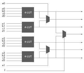
 | Figure 6. Modern FPGA fabric[14-17] |
3. Power Consumption
- Due to the dramatic increase in portable and battery-operated applications, lower power consumption has become a necessity in order to prolong battery life. Power consumption is an important part of the equation determining the end product's size, weight, and efficiency. FPGAs are becoming more attractive for these applications due to their shorter product life cycle. FPGAs are programmable, so they allow product differentiation. Selecting an appropriate FPGA architecture is critical in achieving the best static and dynamic power consumption. As per we are dealing with Power optimization & reduction techniques so before going to study about those techniques first we will discuss about the types of power consumption in modern FPGA. The two components to power consumption: static, dynamic.
3.1. Static Power
- Static power is the power consumed by the FPGA when no signals are toggling. Both digital and analog logic consume static power. The sources of static leakage current in 28-nm transistors are shown in Figure 7. These current which contributes towards leakage power are Isub, subthreshold current when the is in subthreshold region for gate-to-source below the , IG Gate leakage current , IGIDL is a gate-induced drain leakage current and IREV represents for reverse saturation current.
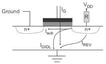 | Figure 7. Sources of Transistor Leakage[19] |
3.2. Dynamic Power
- Dynamic power is the additional power consumed through the operation of the device caused by signals toggling and capacitive loads charging and discharging. As shown in equation 1, the main variables affecting dynamic power are capacitance charging, the supply voltage, and the clock frequency. Dynamic power decreases with Moore’s law by taking advantage of process shrinks to reduce capacitance and voltage. The challenge is that as geometries shrink with each process shrink, the maximum clock frequency increases. While the power reduction declines for an equivalent circuit from process node to process node, the FPGA capacity doubles and the maximum clock frequency increases. The variables affecting dynamic power are explained in equation 1.
 | (1) |
4. Power Reduction Techniques
- The Power Reduction Techniques are developed in various aspects; the power reduction is done at Static (leakage current reduction) power, Dynamic Power reduction through; Glitch removal, Clock Gating, Power Gating, Improved switching activity, Pipelining, Guarded Evaluation etc. we are going to discuss some techniques which are optimized and more efficient. The whole static and dynamic power reduction techniques are divided in three section here that is device, circuit and architectural.
4.1. Device Level Power Reduction Techniques
- FPGA power can be more optimized by using ultra low power devices such as Tunnel-FET, FinFET and other MuGFET[20-28]. These devices are very capable at working on ultra low voltages which would be very efficient for lowering power consumption in FPGA. In this section we are going to discuss about latest advanced devices which would be used to implement FPGA. Circuit design in FPGA will have to cope with enhanced leakage power and large process variability. Using Tunnel-FETs or carbon nanotube transistors instead of MOSFETs could drastically reduce the leakage power. Here we are going to discuss the effects of various advanced devices into digital integrated circuits. Then further we can study how we can use those circuits in FPGA for low power consumption. In this section we are going to discuss the characteristics and expected benefits of some emerging device categories for ultra low power integrated circuits. First, we focus on two categories of sub-thermal subthreshold swing switches Tunnel FETs and carbon nano-tube wires.
4.1.1. Tunnel FET
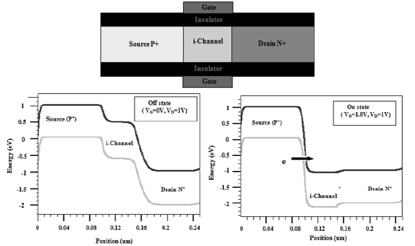
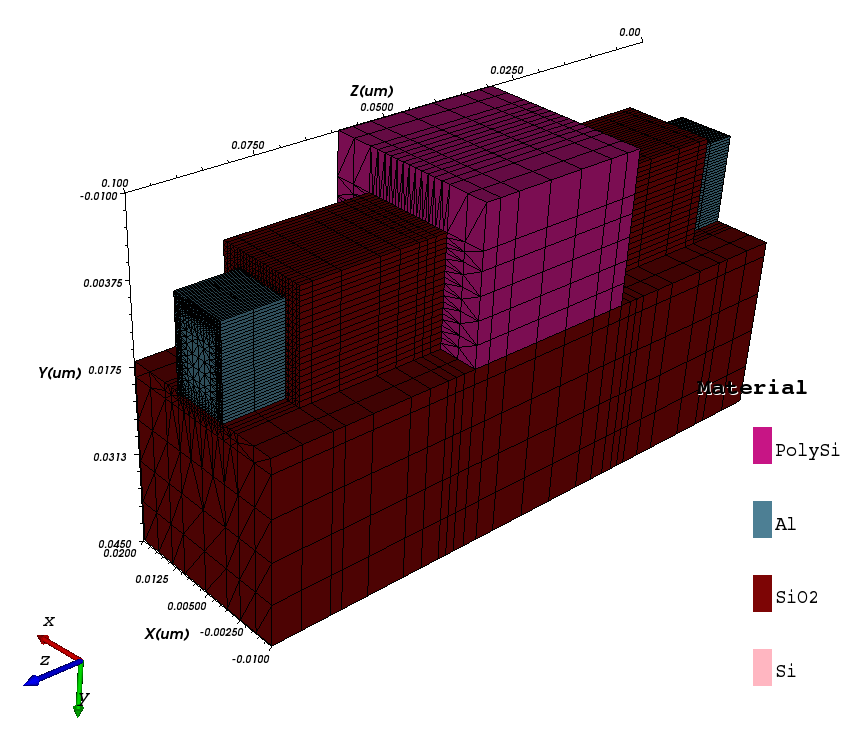
- Tunnel FETs (TFETs) have emerged as most promising candidates for ultra low power digital ICs with voltage supply lower than 0.5V[29]. In contrast to MOSFETs where charge carriers are thermally injected over a barrier, the carrier injection mechanism in a TFET is quantum mechanical band-to-band-tunneling (BTBT). This mechanism is illustrated in the band diagrams of Fig. 8, corresponding to the ON state of the device. The main challenges of TFETs are their low Ion current and extending the low swing over many decades of current. Fig. 9 shows the structure of Tunnel FET made in SILVACO TACD.
 | Figure 8. a) Cross section of an n-type TFET, b) Schematic of energy-band diagram of the OFF-state/ON- state of n-channel DG- TFET[29] |
 | Figure 9. Tunnel FET Structure at visual TCAD Silvaco |
4.1.2. Circuit Design with Tunneling FETs
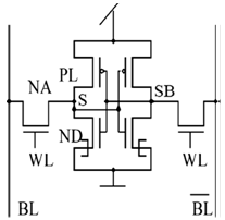
- Since the TFET technology is compatible with CMOS, circuits containing both standard MOSFETs and TFETs can be produced. This allows utilization of TFETs for special purposes, even if full replacement of CMOS cannot be achieved. This is of special interest in novel SOI technologies, which can no longer make use of bipolar devices as in bulk CMOS, and could instead make use of TFETs. In[37, 38] they presented several logic gate structures and an SRAM cell containing a mixture of bulk MOSFETs and planar TFETs. In Fig. 10, we see a six transistor SRAM cell where the two NMOS transistors with the source connected to GND have been replaced by TFETs[39]. Note that in planar bulk TFETs the two word line transistors cannot be replaced, since their source potential is different from GND and would require an additional well. On the other hand, the substrate contact inherent in the TFET source region offers an area advantage in bulk technologies. The read noise margin (RNM) of a SRAM design is estimated graphically as the length of a side of the largest square that can be embedded inside the lobes of a butterfly curve. The Write Noise Margin (WNM) is measured through the write trip point defined as the difference between VDD and the minimum bit-line voltage required to flip the data storage nodes Q or QB. Figure 11 show an example of RNM (Read Noise Margin) measurement, read failure and WNM (Write Noise Margin) for a 6T TFET[40].
 | Figure 10. Static memory cell with two n-MOS, two p-MOS and two TFET transistors[37-39] |
 | Figure 11. a) Measurement of RNM, b) Read failure and WNM[40] |
4.1.3. Leakage Power Reductions from Tunnel FET
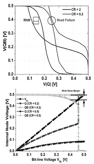
- Due to the inherent nature of TFETs, the OFF state leakage current of a TFET is orders of magnitude lower than CMOS. Thus, we see a huge improvement in terms of leakage reduction[41]. Fig. 12 shows the standby leakage/cell of various SRAM designs. Both 6T and 7T TFET has equal leakage power due to the presence of the same leakage paths. It obtain a 700X and 1600X improvement in leakage reduction over CMOS designs at 0.3V and 0.5V VDD. This shows that TFETs are a potential replacement candidate for CMOS transistors at low voltage and low power applications.
 | Figure 12. Standby leakage/Cell for CMOS and TFET SRAM designs[41] |
4.1.4. Carbon Nano-tube Wires
- A somewhat larger step away from the CMOS mainstream is given by the Carbon Nanotube Field Effect Transistor (CNTFET). In[41] both n-channel and p-channel CNTFETs have been produced using different gate metals and Schottky Barrier source–drain regions. Inverters, ring oscillators, and simple logic gates have been fabricated already[42], but switching speed and ON-current seem still a large step below what is achievable with state-of-the-art CMOS devices[43, 44]. CNTFETs are among the most promising nano devices from the standpoint of their integration into future nano electronic systems on chip. Their physical characteristics (achievable current density, theoretical transition frequency and ratio), as well as their versatility and maturity all argue in favour of this view. They have diameters of typically 1 to 3 nm, but can be several micrometers long. CNTs can be exploited to build both low-resistance high-strength interconnections and highly scalable low-power CNTFETs and single-electron tunnelling transistors[46]. It is possible to consider that CNTFETs can be used to construct logic circuits under two scenarios.
4.1.4.1. Carbon Nanotube in a Transistor Configuration
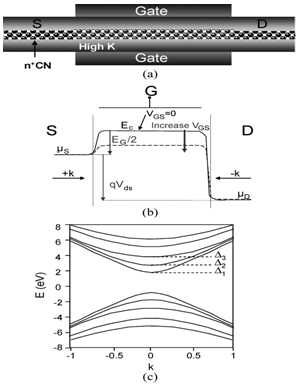 | Figure 13. C-CNTFET, (a) Schematic device features with a high-K dielectric. (b)Band diagram with, at VG=0V, the barrier height at the source–channel junction equal to EG/=2. The source and drain Fermi levels are shown by µSand µD. (c) Energy versus wave number (E- k) diagram[47, 48, 49] |
4.1.5. Carbon Nanotube SRAM Design
- A study of an eight-transistor static random access Memory (SRAM) cell and its implementation in carbon nanotube FET (CNTFET) technology is done by Zhe Zhang et al.[50]. Simulations of the CNTFET SRAM cell design, using a CNT SPICE model, have shown advantages over the CMOS cell in terms of static power, dynamic power, and noise margin. However, current CNT synthesis processes grow metallic CNTs alongside semiconductor CNTs. This in turn greatly degrades the performance and functionality of SRAM cells. They compare two approaches to overcome the presence of metallic CNTs. The first approach tolerates metallic CNTs and uses a series of uncorrelated CNTs to form a transistor; this provides tolerance to metallic CNTs. The second approach uses an M×N array of uncorrelated CNTs to form a CNTFET and requires technologies capable of removing metallic CNTs. Both approaches have similar static noise margin. The second approach (removed metallic CNTs) consumes 1.45× more static power; on the other hand, its CNT count and write delay are reduced to 35.6% and 10.9% of the metallic tolerant approach, respectively. The realization of large memory modules in the presence of faulty SRAM cells can be achieved by having memory modules with as few as two spare columns.
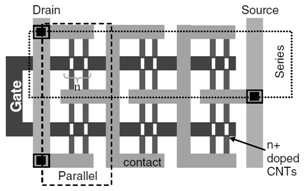 | Figure 14. CNTFET with series–parallel CNTs[50] |
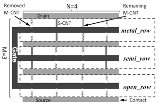 | Figure 15. CNTFET of 3×4 uncorrelated CNTs[50] |
4.2. Circuit Level Power Reduction Techniques
- Static power is dominated by leakage current in various forms: sub-VT leakage, junction leakage i.e., source/drain, well, and triple-well junctions, Gate-Induced Drain Leakage (GIDL) and gate leakage. Here we are going to discuss several leakage current reduction techniques and dynamic power reduction through circuit level approach.
4.2.1. Dual Threshold Transistor Stacking (DTTS)
- This is a technique for static power reduction in nano-scale CMOS circuits[55]. As we know to limit the ever increasing trend of energy and power dissipation in CMOS technology, supply voltage has to be continuously scaled. The amount of power reduction depend not only on supply voltage (VDD) but also on the threshold voltage (Vth) to sustain the reduction of component delay, which is crucial for high speed digital circuit design. Continuous scaling down of these parameters poses several challenges to circuit designers. Particularly threshold voltage reduction leads to increase in sub-threshold leakage current leading to tremendous increase of static power consumption in CMOS circuits, which is otherwise considered as a negligible contributor to the overall power consumption. The performance of a CMOS tri-State buffer using Multi Threshold CMOS (MTCMOS) and Forced Transistor Stacking (FTS) leakage reduction techniques are analyzed and a new technique called Dual Threshold Transistor Stacking (DTTS) for efficient reduction of leakage power is introduced. From the results, it is observed that this technique combines the advantage of multiple threshold and stacking effects in MOSFETs. Table 1 shows the comparison of leakage power between different circuits.
4.2.2. A Dual-threshold FPGA Routing Design
- A dual-threshold FPGA routing design for subthreshold leakage reduction[56] is the technique in which the routing designs are based on the dual-threshold to reduce leakage power. Alternating between buffers and pass transistors, they analyzed the percentage constitution of low-Vth and high-Vth transistors as a function of the leakage reduction and delay increment tradeoff. By routing a suite of Microelectronics Center of North Carolina (MCNC) benchmark circuits, it is shown that an average savings of about 28.83% (as high as 48.46%) in total interconnect leakage can be obtained with 8.73% worst case average delay penalty.
4.2.3. Input Vector Reordering
- A technique of input vector reordering for leakage power reduction in FPGAs[57] which is based on the state dependency property of leakage power. A pin reordering algorithm where the sub-threshold and gate leakage power components are taken into consideration to find the lowest leakage state for the FPGA pass-transistor multiplexers in the logic and routing resources without incurring any physical or performance penalties. This methodology is applied to several FPGA benchmarks, and an average leakage savings of 50.3% is achieved in a 90-nm CMOS process. The trend of leakage current is increasing with the technology scales down which is shown in Fig. 16 and in Fig. 17 it is shown that the leakage current dominant states in FPGA.
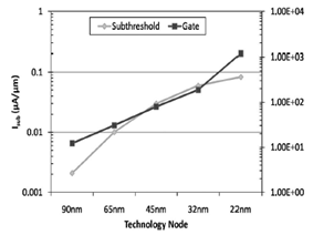 | Figure 16. Leakage current vs. technology[57] |
 | Figure 17. Total leakage-dominant states in FPGA pass-transistor devices (a) 90 nm. (b) 65nm and 45 nm. (c) 32 nm and 22 nm[57] |
4.2.4. FPGA Leakage Power Reduction Using CLB- clustering
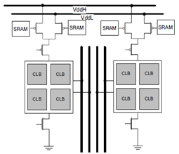
- CLB-clustering design technique employs VDD programmable and power gating methods to reduce leakage in stand-by mode[58]. In compared to the conventional VDD programmable architecture, leakage power of CLB-clustering architecture is 0.1% of the leakage power in no gating FPGA and 8% of leakage power in conventional programmable VDD FPGA. Fig. 18 shows the logic block architecture of the CLB-clustering FPGA[58]. Four CLBs are clustered into one VDD island where the same VDD is used. VDD of the block of 4 CLBs is either high VDD (VDDH) or low VDD (VDDL). The island is applied VDDH when high performance is required and is changed to VDDL if the blocks operate at lower speed. If the number of CLBs decreases in a block, the finer control is possible but area and delay overhead increase. Here, four is selected to keep the chip area and delay overhead below 5%. One CLB includes 4 BLEs and has 5 inputs and 3 outputs. One BLE consists of one LUT, one D-Flip Flop and one 2:1 MUX. This configuration is chosen because it is one of the best configurations for delay, area and logic utilization.
 | Figure 18. Architecture of CLB-clustering[58] |
4.2.5. Programmability of VDD
- Power reduction is of growing importance for field programmable gate arrays (FPGAs). This reduction technique is discussed by Fei Li et al., about programmable supply voltage (VDD) to reduce FPGA power. The FPGA logic fabrics using dual-VDD levels shows that field-programmable power supply is required to obtain a satisfactory power-versus-performance tradeoff. They[59] further design FPGA interconnects fabrics for fine grained VDD programmability with minimal increase of the number of configuration static-random-access-memory cells. With a simple yet practical computer-aided design flow to leverage the field-programmable dual-VDD logic and interconnect fabrics, its carry out a highly quantitative study using placed and routed benchmark circuits, and delay, power, and area models obtained from detailed circuit designs. Compared to single-VDD FPGAs with the VDD level suggested by the ITRS for 100nm technology, field-programmable dual-VDD FPGA reduce the total power by 47.61% and the energy-delay product by 27.36%.
4.3. Architectural Level Power Reduction Techniques
- At architectural level power reduction we have several techniques which will reduce the power in data path, clock gating, and power gating. Some of those power reduction techniques are discussed in this section which will overcome both static and dynamic power.
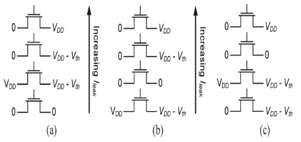
4.3.1. Fine grained-VDD
- Low power FPGA architecture[60] is generated with the use of fine-grained VDD control scheme called micro-VDD-hopping, 4 CLB’s are grouped into one block where VDD is shared as shown in Fig. 19. In the micro-VDD-hopping scheme, VDD of each block is varied between the higher VDD (VDDH) and the lower VDD (VDDL) spatially and temporally to achieve lower power, while keeping performance un-degraded. Simulation using 90nm CMOS technology shows that a leakage power reduction of 95% can be achieved, when this method is used.
 | Figure 19. Schematic of the CLB, four BLE's are clustered into one CLB[60] |
4.3.2. Leakage Reduction in FPGA Routing Multiplexers
4.3.3. Power Gating
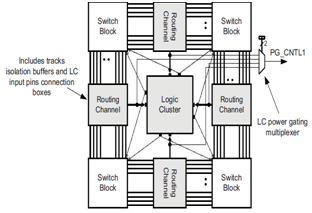 | Figure 20. Dynamic power gating architecture for a logic cluster and its routing channels[62] |
4.3.4. Low Power Programmable FPGA Routing Circuitry
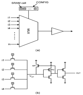
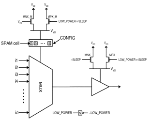
- Programmable FPGA routing[63] technique is for reducing FPGA power consumption, it proposes a family of new FPGA routing switch designs that are programmable to operate in three different modes: high-speed, low-power, or sleep. High-speed mode provides similar power and performance to traditional FPGA routing switches. In low-power mode, speed is curtailed in order to reduce power consumption. Leakage is reduced by 28%-52% in low-power versus high-speed mode, depending on the particular switch design selected. Dynamic power is reduced by 28%-31% in low-power mode. Leakage power in sleep mode, which is suitable for unused routing switches, is 61%-79% lower than in high-speed mode. Fig. 21(a) shows a typical buffered FPGA routing switch[63]. It consists of a multiplexer, a buffer and SRAM con-figuration cells and a transistor-level view of a switch with 4 inputs is shown in Fig. 21(b). NMOS transistor trees are used to implement multiplexers in FPGAs. Routing switch inputs are tolerant to “weak-1” signals. That is, logic-1 in-put signals need not be rail; it is acceptable if they are lower than this. This is due to the level-restoring buffers that are already deployed in FPGA routing switches[see Fig. 21(b)]. It permits such switches to produce “weak-1” signals. The main exceptions to this observation are switches that drive inputs on logic blocks. Based on these three observations,[63] proposed a new switch design shown in Fig. 22. The switch includes n-MOS and p-MOS sleep transistors in parallel (MNX and MPX).
 | Figure 21. Programmable low power routing switch (basic design)[63] |
 | Figure 22. Switch multiplexer with programmable mode[63] |
4.3.5. Clock Gating Power Reduction Technique
- This is the most widely used technique for power reduction. The principle is to stop the clock whenever the device is not in use. Clock gating can be applied to sub-blocks of the design as well as to the whole device. However, correctly stopping the clock is very important. Knowing that the gating logic adds a delay to the clock signal, the effects on setup and hold times must be analyzed. While using clock gating, on FPGAs in particular, the user should take care of the placement of gating logic to minimize delay in the clock network. For reduction of dynamic power through clock gating approach first we discuss about the clock gating architectures for FPGA power reduction[64]. Clock gating is a power reduction technique that has been used successfully in the custom FPGA/ASIC domain. Clock and logic signal power are saved by temporarily disabling the clock signal on registers whose outputs do not affect circuit outputs. By considering and evaluating FPGA clock network architectures with built-in clock gating capability and describe a flexible placement algorithm that can operate with various gating granularities (various sizes of device regions containing clock loads that can be gated together). Results show that depending on the clock gating architecture and the fraction of time clock signals are enabled, clock power can be reduced by over 50%, and results suggest that a fine granularity gating architecture yields significant power benefits. The architectures are illustrated in Fig. 23. Fig. 23(a) shows the REGION architecture where enables are present on switches entering a region. Fig. 23(b) shows the more flexible COLUMN architecture where enables are also present on switches driving vertical spines in logic block columns. Thus, consider a broad range of clock gating architectures with various levels of granularity within clock distribution frameworks that resemble those in commercial chips.
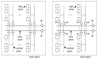 | Figure 23. Clock gating architectures; (a) Enables are present on switches entering a region (b) enables are also present on switches driving vertical spines in logic block columns[64] |
4.3.6. Subthreshold FPGAs
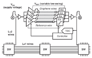
- Sub-threshold operation in CMOS has in recent years become an accepted ultra-low power solution. However, many low-volume applications cannot afford to produce custom silicon. An FPGA, which delivers the flexibility of programming and yet consumes ultra-low power by way of sub-threshold operation, can fill this gap. Field-programmable gate arrays (FPGAs) are an attractive option for low-power systems requiring flexible computing resources. However, the lowest power systems have yet to adopt FPGAs. Subthreshold circuit operation offers the opportunity to operate FPGAs at their minimum energy point. Peter J. Grossmann et al.[65] measured data from an FPGA test chip fabricated in a 0.18-μm SOI process. They showed that the test chip can function at supply voltages as low as 0.26 V without an extra supply for write assists by using latches for configuration bit storage instead of static random access memory. Investigation of the minimum energy point of the FPGA for a high-activity test pattern shows that the minimum energy point of the FPGA can be well below the threshold voltage of the transistors. While Kyeong-Jae Lee et al.[66] demonstrated a subthreshold FPGA system using monolithically integrated graphene wires. The graphene wires replace double-length lines in the interconnect fabric of a custom FPGA implemented in 0.18-μm CMOS. The four-layer graphene wires have lower capacitance than the CMOS aluminium wires, resulting in up to 2.11× faster speeds and 1.54× lower interconnect energy when driven by a low-swing voltage of 0.4 V. They present’s us the first graphene-based system application and experimentally demonstrates the potential of using low capacitance graphene wires for ultralow power electronics.
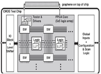 | Figure 24. Overview of FPGA test chip. Graphene wires are integrated on top of the CMOS chip and interface to the switch matrices (SW). Only a portion of the logic array and switch matrices are shown[66] |
 | Figure 25. Diagram of graphene interface |
5. Conclusions and Future Work
- Due to the dramatic increase in power conscious applications and tighter power budgets, there is a necessity of low power consumption systems. The use of FPGA technology in low-power applications is increasing now-a-days, which makes achieving low power systems an increasingly important challenge. FPGAs have been adopted widely in recent years due to advanced technology that lowered the unit price, but the reduction in price have come at the cost of higher power due to higher transistor leakage. Various FPGA technologies have significantly different power profiles, and these differences can have a profound impact on the overall system design and power budget. Power consumption in FPGAs has become a primary concern for FPGA selection as previously more focus was on speed and making device more compact. But due to regressive use of mobile and portable devices human beings indirectly consume power from the nature as we are utilizing the power in the devices through natural resources like wind, water and other natural resources. According to Moore’s law, the device size reduces half of its present size in every 1.5 years. With reduced size, system will be faster and compact, but high end devices require lots of battery and natural power to run. So there is a need to focus on Power savings and to develop more refined and more optimize devices which can work on low power.This paper is focused on Device, Circuit & Architectural Techniques for ultra-low power FPGA design. We discussed various power models for accurately computing the static and dynamic power both. We explore a strong review of various power reduction techniques and finds out the best technique for static and dynamic power. The techniques used for static power reduction reduces power upto 60-90% and dynamic power reduction techniques reduces power upto 30-50%. In static power reduction, dual-VT FPGA architecture is explored and it indicates an average leakage power savings of upto 64%. In case of dynamic power, power savings of upto 61.6% can be achieved using LOPASS Technique[68] and upto 30% and 50% with clock gating and Glitch reduction techniques[69] respectively. Table 2 and table 3 shows the static & dynamic power results and various comparisons between them.
|
|
References
| [1] | Xilinx, “Lowering power at 28 nm with Xilinx 7 Series FPGAs”, White paper WP389 (v1.1.1), 2012. |
| [2] | Actel, “Dynamic power reduction in Flash FPGAs”, White paper, 2011. |
| [3] | Xilinx (2011), “Power methodology guide,” White paper, UG786 (v13.1). |
| [4] | Kuon and J. Rose, “Measuring the gap between FPGAs and ASICs”, ACM/SIGDA, International symposium on Field Programmable Gate Arrays, pp. 21-30, 2006. |
| [5] | V. Betz., J. Rose, and A. Marquardt, “Architecture and CAD for deep-submicron FPGAs”, Kluwer academic publishers, 1999. |
| [6] | S.J.E. Wilton, J. Rose, and Z.G. Vranesic, “Architecture of centralized field-configurable memory, ACM/SIGDA International symposium on Field- Programmable Gate Arrays (FPGA)”, pp. 97-103, 1995. |
| [7] | S. Hong and S.S. Chin, “Reconfigurable embedded MAC core design for low-power coarse grain FPGA”, IET Electronics Letters, Volume 39, Issue 7, pp. 606-608, 2003. |
| [8] | G. Lemieux and D. Lewis, “Design of interconnection networks for programmable logic”, Springer (formerly Kluwer Academic Publishers), 2004. |
| [9] | International Technology Roadmap for Semiconductors, 2011. |
| [10] | Ahmed, Elias and Jonathan Rose, “The effect of LUT and cluster size on deep-submicron FPGA performance and density”, ACM Symposium on FPGAs, pp. 3-12, 2000. |
| [11] | Lewis, D., et al., “The Stratix II logic and routing architecture, ACM symposium on FPGAs”, 14-20, 2005. |
| [12] | Altera, “White paper on, FPGA architecture”, ver. 1.0, 2006. |
| [13] | V. Betz, J. Rose and A. Marquardt, “Architecture and CAD for deep-submicron FPGAs”, Kluwer Academic Publishers, 1999. |
| [14] | B. Zahiri, “Structured ASICs: Opportunities and challenges”, International conference on computer design, pp. 404-409, 2003. |
| [15] | R. R. Taylor and H. Schmit, “Creating a Power-aware structured ASIC”, International symposium on low power electronics and design, pp. 74-77, 2004. |
| [16] | K. J. Han, et al., “Flash-based Field Programmable Gate Array Technology with deep trench isolation”, IEEE Custom integrated circuits conference, pp. 89-91, 2007. |
| [17] | S. D. Brown, “An overview of Technology, Architecture and CAD tools for programmable logic devices”, IEEE Custom integrated circuits conference, pp. 69-76, 1994. |
| [18] | J. Greene, E. Hamdy, and S. Beal, “Antifuse Field Programmable Gate Arrays”, IEEE Transactions on Very Large Scale Integration (VLSI) Systems, Volume 81, Issue 7, pp. 1042-1056, 1993. |
| [19] | Altera, “White paper on reducing power consumption and increasing bandwidth on 28-nm FPGAs”, WP-01148-2.0, 2012. |
| [20] | PIDS Working Group, “Results and Issues”, ITRS 2007 public conference. |
| [21] | Thean Av-Y, Shi Z-H, Mathew L, Stephens T, Desjardin H, Parker C, et al., “Performance and variability comparisons between multi-gate FETs and planar SOI transistors”, IEDM, 2006. |
| [22] | Kavalieros J, et al., “Tri-gate transistor architecture with high k gate dielectrics metal gates and strain engineering”, VLSI technology symposium, 2006. |
| [23] | Satish Kumara, et al., “Self-consistent and efficient electro-thermal analysis for poly/metal gate fin-FETs”, VLSI technology symposium, 2006. |
| [24] | Inaba, et al., “The prospective multi gate device for future SoC applications”, ESSDERC, 2006. |
| [25] | Park Jong-Man, Han Sang-Yeon, Jeon Chang-Hoon, Sohn Si-Ok, Lee Jun-Bum,Yamada Satoru, et al. ,“Fully integrated advanced bulk FinFETs architecture featuring partially-insulating technique for DRAM cell application of 40 nm generation and beyond,” IEDM, 2006. |
| [26] | Von Arnim K, et al., “A low-power multi-gate FET CMOS technology with 13.9 ps inverter delay”, VLSI technology symposium, 2007. |
| [27] | Fulde M, Arnim K. V., Pacha C, Bauer F, Russ C, Sipra D., et al., “Advances in multigate MOSFET circuit design”, ICECS, 2007. |
| [28] | Collaert, et al., “Performance enhancement of MUGFET devices using Super Critical Strained–SOI (SC-SSOI) and CESL”, VLSI Technology Symposium, 2006. |
| [29] | Adrian M. Ionescu, et al., “Ultra low power: emerging devices and their benefits for Integrated Circuits”, Electron Devices Meeting (IEDM), IEEE International, pp. 16.1.1 - 16.1.4, 2011. |
| [30] | W. M. Reddick and G. A. J. Amaratunga, “Silicon surface tunnel transistor”, Applied Physics Letters, Volume 67 Issue 4, pp. 494-496, 1995. |
| [31] | D. Kim, Y. Lee, J. Cai, I. Lauer, L. Chang, S. J. Koester, D. Sylvester, and D. Blaauw, “Low power circuit design based on hetero-junction tunneling transistors”, in ISLPED ’09: Proceedings of the 14th ACM/IEEE international symposium on Low power electronics and design. New York, USA: ACM, pp. 219–224, 2009. |
| [32] | P. Nilsson, “Arithmetic reduction of the static power consumption in nanoscale CMOS”, IEEE International Conference on Electronics, Circuits and Systems, pp. 656-659, 2006. |
| [33] | B. Van Zeghbroeck. Principles of Semiconductor Devices, online at , 2007. |
| [34] | D. Kim, Y. Lee, J. Cai, I. Lauer, L. Chang, S. J. Koester, D. Sylvester, and D. Blaauw, “Low power circuit design based on heterojunction tunneling transistors”, ISLPED ’09: Proceedings of the 14th ACM/IEEE international symposium on Low power electronics and design. New York, pp. 219–224, 2010. |
| [35] | B. Yang, K. D. Buddharaju, S. H. G. Teo, N. Singh, G. Q. Lo, and D. L. Kwong, “Vertical silicon-nanowire formation and gate-all-around MOSFET”, IEEE Electron Device Letter, Volume 29, Issue 7, pp. 791–794, 2008. |
| [36] | B. Yu, L. Chang, S. Ahmed, H. Wang, S. Bell, C. Y. Yang, C. Tabery, C. Ho, Q. Xiang, T. J. King, J. Bokor, C. Hu, M. R. Lin, And D. Kyser , “FinFET scaling to 10 nm gate length, , pp. 251–254, 2002. |
| [37] | Nirschl T, et al., “The Tunneling Field Effect Transistor (TFET) as an add-on for ultra-low-voltage analog and digital processes”, IEDM, 2007. |
| [38] | Nirschl T, Weis M, Fulde M, Schmitt-Landsiedel D, “ Revision of the tunneling field-effect transistor in standard CMOS technologies”, IEEE Electron Device Letter Volume 28, Issue 4, 195-198. |
| [39] | J. Singh et al., “A Novel Si-Tunnel FET based SRAM Design for Ultralow-Power 0.3V VDD Applications,” Design Automation Conference (ASP-DAC), 2010. |
| [40] | Nirschl T., “Circuit applications of the tunneling field effect transistor (TFET)”, Dissertation Technische Universität München, 2007. |
| [41] | Chen Z et al., “Gate work function engineering for nanotube-based circuits”, ISSCC, 2007. |
| [42] | Deng J, Patil N, Ryu K, Badmaev A, Zhou C, Mitra S et al. ,“Carbon nanotube transistor circuits: circuit-level performance benchmarking and design options for living with imperfections”, In: Proc ISSCC, pp. 70-588, 2007. |
| [43] | O’connor Ian, et al., “CNTFET modeling and reconfigurable logic circuit design”, IEEE Transaction Circuit System, Volume 54, Issue 11, pp. 65–79, 2007. |
| [44] | Pourfath M, Kosina H, Selberherr S., “The role of inelastic electron–phonon interaction on the on-current and gate delay time of CNT-FETs”, ESSDERC, 2007. |
| [45] | D. Rondoni and J. Hoekstra, “Towards models for CNT devices,” Proc. IEEE RISC’05, 2005, pp. 272–278. |
| [46] | S. J. Wind, J. Appenzeller, and P. Avouris, “Lateral scaling in carbon nanotube field-effect transistors,” Phys. Rev. Lett., vol. 91, no. 5, pp.058301-1–058301-4, Aug. 2003. |
| [47] | P. Avouris, J. Appenzeller,R.Martel, and S. J.Wind, “Carbon nanotube electronics,” Proc. IEEE, vol. 91, no. 11, pp. 1772–1784, Nov. 2003. |
| [48] | R. Saito, M. S. Dresselhaus, and G. Dresselhaus, Physical Properties of Carbon Nanotubes. London, UK, U.K.: Imperial College Press, 1998. |
| [49] | Zhe Zhang and Jos´e G. Delgado-Frias “Carbon Nanotube SRAM Design With Metallic CNT or Removed Metallic CNT Tolerant Approaches,” IEEE Transactions on Nanotechnology, Vol. 11, No. 4, July 2012 |
| [50] | A. Lin, N. Patil, H. Wei, S. Mitra, and H.-S. P. Wong, “A Metallic-CNT Tolerant carbon nanotube technology using asymmetrically-correlated CNTs (ACCNT),” in Proc. Symp. VLSI Technol., 2009, pp. 182–183. |
| [51] | G. Zhang, P. Qi, X.Wang, Y. Lu, X. Li, R. Tu, S. Bangsaruntip, D. Mann, L. Zhang, and H. Dai, “Selective etching of metallic carbon nanotubes by gas-phase reaction,” Science, vol. 314, pp. 974–977, 2006. |
| [52] | N. Patil, A. Lin, J. Zhang, H. Wei, K. Anderson, H.-S. P. Wong, and S. Mitra, “VMR: VLSI-compatible metallic carbon nanotube removal for imperfection-immune cascaded multi-stage digital logic circuits using carbon nanotube FETs,” in Proc. IEEE Int. Electron Devices Meeting Dec. 7–9, 2009, pp. 1–4. |
| [53] | E. Pop, “The role of electrical and thermal contact resistance for joule breakdown of single-wall carbon nanotubes,” Nanotechnology, vol. 19, no. 295202, pp. 1–5, 2008. |
| [54] | R. Udaiyakumar and K. Sankaranarayanan, “Dual Threshold Transistor Stacking (DTTS) - A novel technique for static power reduction in nano-scale CMOS circuits”, European Journal of Scientific Research, Volume 72 Issue 2, pp. 184-194, 2012. |
| [55] | Rodrigo Jaramillo-Ramirez and Mohab Anis, “A dual-threshold FPGA routing design for sub-threshold leakage reduction”, IEEE international symposium on circuits and systems, 2007. |
| [56] | Hassan et al., “Input vector reordering for leakage power reduction in FPGAs”, IEEE Transactions on Computer aided design of integrated circuits and systems, Vol. 27, Issue 9, pp. 1555 – 1564, 2008. |
| [57] | Mohammad Mehdi Tohidi and Nasser Masoumi, “FPGA leakage power reduction using CLB-clustering technique, IEEE Nanoelectronics Conference (INEC), pp. 637 – 638, 2010. |
| [58] | Fei Li, et al. ,“Field programmability of supply voltages for FPGA power reduction”, IEEE Transactions on Computer-Aided Design of Integrated Circuits and Systems, Volume 26 Issue 4, pp. 752 – 764, 2007. |
| [59] | Canh Q. Tran, et al., “95% Leakage reduced FPGA using zigzag power-gating, Dual-VTH/VDD and Micro VDD hopping”, IEEE , 2005. |
| [60] | Mohd. Hasan, A.K. Kureshi, “Leakage reduction in FPGA routing multiplexers”, IEEE international symposium on circuits and systems, 2009. |
| [61] | Assem A. M. Bsoul and Steven J. E. Wilton, “An FPGA architecture supporting dynamically controlled power gating”, IEEE international conference on |
| [62] | Jason H. Anderson, et al., “ Low-Power programmable FPGA routing circuitry”, IEEE Transactions on Very Large Scale Integration (VLSI) Systems, Volume 17, Issue 8, pp. 1048 – 1060, 2009. |
| [63] | Safeen Huda, Muntasir Mallick, Jason H. Anderson, “Clock gating architectures for FPGA power reduction”, IEEE , 2009. |
| [64] | Peter J. Grossmann et al., “Minimum Energy Analysis and Experimental Verification of a Latch-Based Subthreshold FPGA,” IEEE Transactions on Circuits and Systems-II: Ex-press Briefs, Vol. 59, No. 12, December 2012. |
| [65] | Kyeong-Jae Lee, Hyesung Park, Jing Kong, and Anantha P. Chandrakasan, “Demonstration of a Subthreshold FPGA Using Monolithically Integrated Graphene Interconnects”, IEEE Transactions on Electron Devices, Vol. 60, No. 1, January 2013. |
| [66] | Rajsaktish Sankaranarayanan, Matthew R. Guthaus, “A Single-VDD Ultra-Low Energy Sub-threshold FPGA,” IEEE 20th International Conference on VLSI and System-on-Chip (VLSI-SoC), 2012. |
| [67] | Deming Chen, et al., “ LOPASS: A Low-Power architectural synthesis systems for FPGAs with interconnect estimation and optimization,” IEEE Transactions on Very Large Scale Integration (VLSI) Systems, Volume 18, Issue 4, pp. 564 – 577, 2010. |
| [68] | Anand Raghunathan, et al., “Register transfer level power optimization with emphasis on glitch analysis and reduction,” IEEE Transactions on computer-aided design of integrated circuits and systems, Volume 18 Issue 8, pp. 1114 – 1131, 1999. |
| [69] | Chirag Ravishankar, et al., “FPGA power reduction by guarded evaluation considering logic architecture,” IEEE Transactions on Computer-Aided Design of Integrated Circuits and Systems, Vol. 31, No. 9, September 2012. |