-
Paper Information
- Next Paper
- Previous Paper
- Paper Submission
-
Journal Information
- About This Journal
- Editorial Board
- Current Issue
- Archive
- Author Guidelines
- Contact Us
American Journal of Materials Science
p-ISSN: 2162-9382 e-ISSN: 2162-8424
2015; 5(3A): 39-47
doi:10.5923/s.materials.201502.07
High Energy Radiation Effects on the Seebeck Coefficient, van der Pauw-Hall Effect Parameters and Optical Properties of Si/Si+Sb Multi-Nanolayered Thin Films
 Abstract
 Reference
 Full-Text PDF
 Full-text HTML
S. Budak1, E. Gulduren2, B. Allen1, J. Cole1, J. Lassiter3, T. Colon4, C. Muntele5, R. Parker6, C. Smith7, R. B. Johnson1, 4
1Department of Electrical Engineering & Computer Science, Alabama A&M University, Normal, AL USA
2Department of Physics, University of Alabama in Huntsville, Huntsville, AL USA
3Materials Research Laboratory, Alabama A&M University, Normal, AL USA
4Department of Physics, Chemistry, and Mathematics, Alabama A&M University, Normal, AL USA
5Cygnus Scientific Services, Huntsville, AL USA
6Marshall Flight and Space Center, Huntsville, AL USA
74 SIGHT INC. Huntsville, AL USA
Correspondence to: S. Budak, Department of Electrical Engineering & Computer Science, Alabama A&M University, Normal, AL USA.
| Email: |  |
Copyright © 2015 Scientific & Academic Publishing. All Rights Reserved.
We have prepared thermoelectric devices from alternating layers of Si/Si+Sb superlattice films using the electron beam deposition (EBD). In order to determine the stoichiometry of the elements and the thickness of the grown multi-layer film, Rutherford Backscattering Spectrometry (RBS) and RUMP simulation have been used. The 5 MeV Si ions bombardments have been performed using the AAMU Pelletron ion beam accelerator, to form quantum clusters in the multi-layer superlattice thin films to improve the thermoelectric and optical properties for more efficient thermoelectric devices. The fabricated multilayered thermoelectric devices have been characterized using cross plane electrical conductivity and Seebeck coefficient, van der Pauw resistivity, density, mobility, Hall coefficient, optical absorption, photoluminescence (PL), Raman, and AFM measurements. High-energy ion beam modification caused some remarkable thermoelectric and optical properties.
Keywords: Ion bombardment, Seebeck coefficient, Multi-Nanolayers, Figure of merit, van der Pauw resistivity, Hall Effect
Cite this paper: S. Budak, E. Gulduren, B. Allen, J. Cole, J. Lassiter, T. Colon, C. Muntele, R. Parker, C. Smith, R. B. Johnson, High Energy Radiation Effects on the Seebeck Coefficient, van der Pauw-Hall Effect Parameters and Optical Properties of Si/Si+Sb Multi-Nanolayered Thin Films, American Journal of Materials Science, Vol. 5 No. 3A, 2015, pp. 39-47. doi: 10.5923/s.materials.201502.07.
Article Outline
1. Introduction
- The use of waste heat from mobile and stationary energy conversion processes to optimize power generation (cars: substitution of the alternator; power plants and combined heat and power production: power production plus), and also to optimize combustion in simple wood stoves (electric-driven fans for air supply) is considered promising fields of application [1]. Thermoelectric generators (TEG) can convert waste heat into electric energy without using moving parts and without producing carbon dioxide gas, toxic substances or other emissions. It is expected that thermoelectric power generation can provide a new energy source from the conversion of waste heat emitted by automobiles, factories, and other similar sources [2]. Earlier studies of thermoelectric materials and their applications were based on bulk materials. However, with the increasing combination of a higher heat flux with a higher package density in microelectronic devices, it is becoming more challenging to provide sufficient heat dissipation from the package. Therefore, thin film thermoelectric devices with an efficient cooling capacity, small area, and short response time are in high demand. The efficiency per unit area of thermoelectric devices made of thin films is higher than that of devices made of bulk materials, and thin film thermoelectric devices can be applied in more diverse fields [3]. In general, a TEG consists of a number of semiconductor pairs that are connected electrically in series and thermally in parallel, and each pair includes a p-type and an n-type element. Although in theory, a single piece of semiconductor material could work, a series connection is used to meet the high voltage potential requirements. P-type and n-type elements are alternated to assure that the carriers transport in the same direction [4]. In most of the power generation applications, the figure of merit is on the order of 1 resulting in low device thermal efficiency. Although the research into thermoelectric material development for high figure of merit is progressing, the maximum device thermal efficiency is still on the order of less than 10% [5]. In order to improve the thermoelectric properties of thermoelectric materials, thin film technique is used due to the stronger quantum confinement compared to that of their bulk materials [6]. A combination of recent significant advances in the scientific understanding of quantum wells, nanostructure effects on thermoelectric (TE) properties, and modern thin-layer and nano-scale manufacturing technologies have produced the advanced TE materials with potential conversion efficiencies of over 15%. The advent of these advanced TE materials offers new opportunities to recover waste heat more efficiently and economically with highly reliable and relatively passive systems that eliminate noise and vibration. A TEG device produces voltage when a temperature difference (DT) occurs between the two sides of the device because of the thermoelectric effect [7]. With the help of the technology of quantum-well super-lattices, quantum-dot super-lattices, nano-tubes, etc., nano-structured thermoelectric devices could provide the possibility of substantially increasing the thermoelectric figure of merit. It may be expected that micro-/nano-scaled heat engines will be one of the important applications in nano-technology in the near future [8]. Many interdisciplinary areas like physics, chemistry, and material sciences are developing so rapidly. Ion induced modifications of solids, thin films, surface and interfaces are such fields emerged as areas to quantify the properties of solids up to a shallow depth [9]. The efficiency of the thermoelectric materials and devices, the figure of merit is defined by
 , where S is the Seebeck coefficient, σ is the electrical conductivity, T is the absolute temperature, and κ is the thermal conductivity. ZT could be increased by increasing S, by increasing σ, or by decreasing κ. In order to compete with conventional refrigerators, a ZT of 3 is required. Due to their limited energy conversion efficiencies (i.e. ZT is ~ 1); thermoelectric devices currently have a rather narrow set of applications [10, 11]. Some of the previous works [12-16] focused on Si-Ge thin film systems, which were either SiGe single layered thin film, Si/Si+Ge multilayered superlattice thin film or (because of the preceding ‘either’) Si/Ge multilayered thin film systems. We have reached remarkable thermoelectrical and optical properties from those studies. These results and some of our Sb results from our other studies encouraged us to work on Si/Si+Sb multilayered thin film systems. In this study, we reported the growth of Si/Si+Sb multilayer superlattice films using the electron beam deposition (EBD) and performed thermoelectrical and optical characterizations. The produced thin films were bombarded with high-energy Si ions for increasing cross plane electrical conductivity, decreasing van der Pauw resistivity, and tailoring carrier density, mobility, and Hall coefficient. In addition to those measurements, we have also performed some optical characterizations like optical absorption, photoluminescence (PL), Raman, and Atomic Force Microscopy (AFM) measurements. We will be continuing the in-plane and cross-plane thermal conductivity measurements in our future studies with our new Laser PIT thermal conductivity and 3w thermal conductivity measurement systems.
2. Experimental
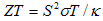
- We have deposited the Si/Si + Sb multi-nano-layered films on silicon and silica (suprasil) substrates using the electron beam deposition (EBD). Silica (suprasil) substrate is used for optical absorption, photoluminescence and Seebeck coefficient measurements, 100 nm oxidized Si substrates are used for the electrical conductivity measurements, Raman, and AFM measurements. Multilayer thin film systems have been prepared as 20 or 50 multilayered structures. 20 and 50 multilayers were sequentially deposited to have 10 and 25 periodic structures consisting of alternating Si and Si + Sb layers. The base pressure obtained in the chamber was about 3x10⁻⁶ Torr. A gold-coated INFICON quartz crystal microbalance (QCM) monitor was used to monitor the growth rate during the multilayer deposition. The film geometries used for deposition of Si/Si + Sb multi-nano-layers to apply the cross plane electrical and optical measurements are shown in Fig. 1. Pelletron ion beam accelerator at the Alabama A&M University, Materials Research Laboratory (AAMU-MRL) was used to bombard the multi-nano-layered Si/Si+Sb thin films at the energies of 2 and 5 MeV for 20 and 50 multilayers to form nano-dots and /or nano-clusters to increase the electrical conductivity and Seebeck coefficients, and change the optical properties. In this study, we do not have the thermal conductivity measurements.
 | Figure 1. Geometry (a) for the cross plane Seebeck coefficient and electrical conductivity, (b) for van der Pauw-Hall Effect measurements and for the optical absorption and photoluminescence measurements |
 and
and  . Rutherford Backscattering Spectrometry (RBS) was performed using 2.1 MeV He+ ions with particle detector placed at 170 from the incident beam to monitor the elemental analysis [17-19]. The optical absorption spectra of films were recorded in the range 200 – 800 nm with a CARY 5000 UV–Vis–NIR spectrophotometer. The photoluminescence (PL) measurements were performed on a CARY Eclipse Spectrometer at an excitation wavelength of 350 nm.
3. Results and Discussion
- Figure 2 shows the cross plane electrical conductivity measurements for 20 alternating layers of Si/Si + Sb multi-nano-layered thin films depending on the applied 2 MeV Si ions bombardment fluences. As seen from the figure 2, the electrical conductivity started to decrease when the first ion bombardment fluence of
 was introduced and then the electrical conductivity increased until the fluence of
  . After the fluence of
 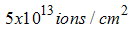 , the electrical conductivity decreased again. First decrease in the electrical conductivity could arise from the thermal stabilization after the high-energy beam was introduced. After the thermal stabilization, the increase in the charge carrier concentration could cause an increase in the electrical conductivity. Applied high-energy beam did not affect too much the cross plane electrical conductivity in the increasing direction. High electrical conductivity is one of the desired things for the high efficient thermoelectric devices and materials. Si ions bombardment could increase the charge carrier concentration and could cause an increase in the electrical conductivity.
  | Figure 2. Fluence dependence of the cross- plane electrical conductivity of 20 alternating layers of Si/Si+Sb thin films |
 and
and  . This interval might be good for this film system. Forming nano-structuring could cause higher electrical conductivity [20].Figure 3 shows the fluence dependence of optical absorption spectra of 20 alternating layers of Si/Si+Sb thin films. As seen from the figure 3, the optical absorption spectra look like each other except for the shifting in y-direction. But the relative amplitudes as a function of wavelength almost stay unchanged. There are three absorption peaks that appeared at 350, 550, and 640 nm from the 20 alternating Si/Si+Sb multilayer thin films. These absorption peaks were labeled on the figure 3. Zhong et al. (2014) found the optical absorption peak for Sb at 566 nm. What we got at 550 nm and 640 nm could come from Sb nanoparticles in the thin film system [21]. Eckhoff et al. (2005) showed the optical absorption from the Si nano-particles at about 280 nm. Our peak in the graph at 350 nm could come from Si nanoparticles from the multilayer thin film [22].
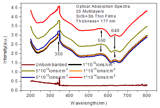 | Figure 3. Fluence dependence of optical absorption spectra of 20 alternating layers of Si/Si+Sb thin films |
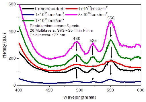 | Figure 4. Fluence dependence of photoluminescence spectra of 20 alternating layers of Si/Si+Sb thin films |
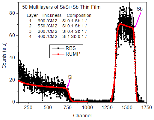 | Figure 5. RBS and RUMP graphs of 50 alternating layers of Si/Si+Sb thin films |
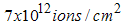 , the Seebeck value started to decrease. Depending on the material systems, the high energy ions beam bombardment might have an effect to increase the Seebeck coefficients since the ion beam bombardment could increase the charge carrier concentration in the thin film systems. Even the Seebeck coefficient increases in negative direction due to the type of materials like n-type and p-type semiconductors, the figure of merit increases due to the square of the Seebeck coefficient in the figure of merit equation.
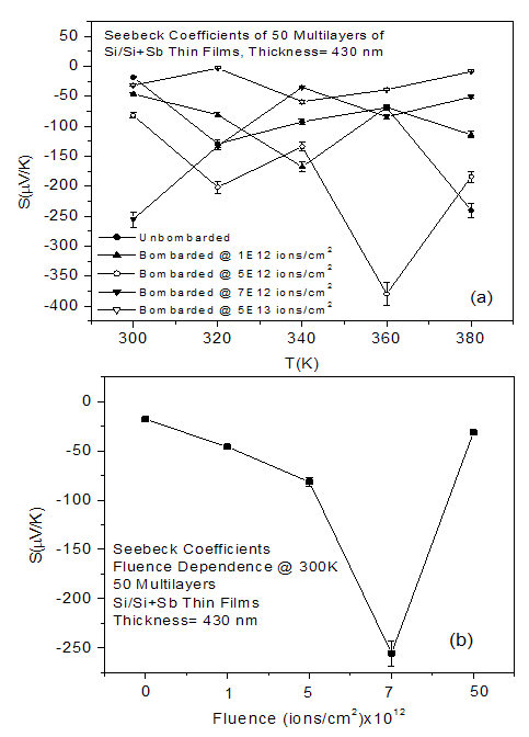 | Figure 6. Fluence dependence of the cross-plane Seebeck coefficient of 50 alternating layers of Si/Si+Sb thin films (a) at the different temperatures, (b) at room temperature |
 | Figure 7. Fluence dependence of the van der Pauw resistivity measurements of 50 alternating layers of Si/Si+Sb thin films at the different temperatures |
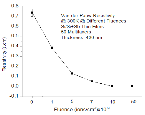 | Figure 8. Fluence dependence of the van der Pauw resistivity measurements of 50 alternating layers of Si/Si+Sb thin films at the room temperature |
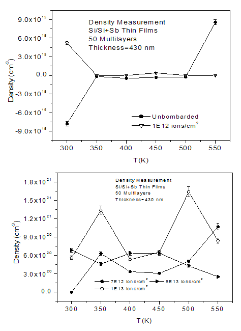 | Figure 9. Fluence dependence of the density measurements of 50 alternating layers of Si/Si+Sb thin films at the different temperatures |
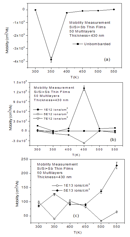 | Figure 10. Fluence dependence of the mobility measurements of 50 alternating layers of Si/Si+Sb thin films at the different temperatures |
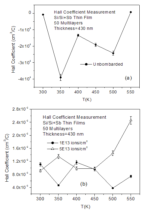 | Figure 11. Fluence dependence of the Hall coefficient measurements of 50 alternating layers of Si/Si+Sb thin films at the different temperatures |
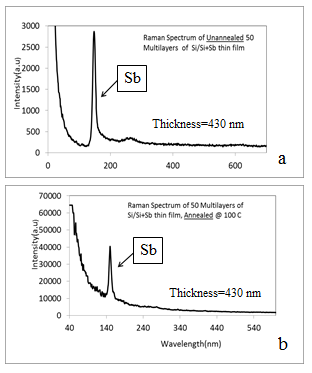 | Figure 12. Raman spectra of 50 alternating Si/Si+Sb multilayer thin films: a) Unannealed and b) annealed at 100°C |
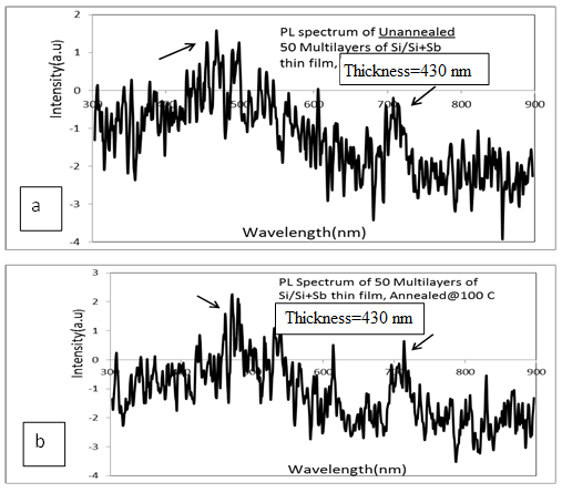 | Figure 13. Photoluminescence Spectra of 50 alternating Si/Si+Sb multilayer thin films: a) Unannealed and b) annealed at 100°C |
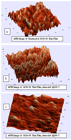 | Figure 14. Temperature dependence AFM images of 50 alternating multilayer Si/Si+Sb thin films |
4. Conclusions
- Multilayer thin film systems from Si/Si+Sb have been deposited as 20 and 50 multilayer thermoelectric devices. The prepared thermoelectric devices were then introduced by high energy Si ions bombardment to form nano-dots and /or nano-clusters to tailor the thermoelectric and optical properties. Seebeck coefficient, van der Pauw resistivity measurements showed remarkable results at the suitable fluences as expected from the high efficient thermoelectric devices and materials. Transport properties addition to the van der Pauw resistivity like mobility, density, and Hall coefficient measurements showed shifting from n-type structure to p-type semiconductor structure. This might be arising from the charge carrier concentration due to high energy Si ion beam bombardment. AFM results show some smoothness on the surfaces depending on the annealing temperature. Further studies were planned in addition to the thermal conductivity measurements on S/Si+Sb thin film systems to reach more efficient thermoelectric devices.
ACKNOWLEDGEMENTS
- Research sponsored by Materials Research Laboratory (MRL), National Science Foundation under NSF-EPSCOR R-II-3 Grant No. EPS-1158862, DOD under Nanotechnology Infrastructure Development for Education and Research through the Army Research Office # W911 NF-08-1-0425, and DOD Army Research Office # W911 NF-12-1-0063, U.S. Department of Energy National Nuclear Security Admin with grant# DE-NA0001896 and grant# DE-NA0002687, NSF-REU with Award#1156137.