-
Paper Information
- Next Paper
- Previous Paper
- Paper Submission
-
Journal Information
- About This Journal
- Editorial Board
- Current Issue
- Archive
- Author Guidelines
- Contact Us
American Journal of Materials Science
p-ISSN: 2162-9382 e-ISSN: 2162-8424
2015; 5(3A): 31-35
doi:10.5923/s.materials.201502.05
Thermal Annealing Effects on the Thermoelectric and Optical Properties of SiO2/SiO2+Au Multilayer Thin Films
 Abstract
 Reference
 Full-Text PDF
 Full-text HTML
S. Budak, S. Yang, Z. Xiao, R. B. Johnson
Department of Electrical Engineering & Computer Science, Alabama A&M University, Normal, AL USA
Correspondence to: S. Budak, Department of Electrical Engineering & Computer Science, Alabama A&M University, Normal, AL USA.
| Email: |  |
Copyright © 2015 Scientific & Academic Publishing. All Rights Reserved.
Thermoelectric thin films have been prepared from 100 alternating layers of SiO2/SiO2+Au superlattice films using Magnetron DC/RF Sputtering. Scanning Electron Microscope (SEM) and Energy Dispersive Spectroscopy (EDS) have been used to analyze the surface and composition of the thin films. In order to form nano-structures (nano-dots and/or nano-clusters) in the multilayers, the fabricated thin films were annealed at different temperatures ranging between 100°C and 400°C. The thin films annealed at different temperatures have been characterized using Seebeck coefficient measurement, van der Pauw resistivity measurement, mobility, density, Hall Effect measurements, Optical absorption spectroscopy, SEM and EDS analysis, and Atomic Force Microscopy (AFM). The Seebeck coefficient reached its highest value for the sample annealed at 500°C when the measurement temperature reached 360 K. The highest Seebeck coefficient was recorded as about -425 µV/K at 360 K. The resistivity values increased when it was annealed at 100°C, and then decreased and reached the lowest value when the annealing temperature reached the 200°C. Temperature annealing affected the negative mobility and Hall Effect coefficients to shift to the positive direction. The optical absorption spectra got narrower when the annealing temperatures increased. SEM shows that the surface of the multilayer thin films is very smooth.
Keywords: Thermal annealing, Thermoelectric and optical properties, Multi-Nanolayers, Figure of merit
Cite this paper: S. Budak, S. Yang, Z. Xiao, R. B. Johnson, Thermal Annealing Effects on the Thermoelectric and Optical Properties of SiO2/SiO2+Au Multilayer Thin Films, American Journal of Materials Science, Vol. 5 No. 3A, 2015, pp. 31-35. doi: 10.5923/s.materials.201502.05.
Article Outline
1. Introduction
- Thermoelectric materials are increasingly becoming more important due to their applications in thermoelectric power generation as heat harvesting and microelectronic cooling devices [1, 2]. The theory of thermoelectric power generation and thermoelectric refrigeration was first presented by Altenkirch in 1990 [3]. The efficiency of the thermoelectric devices and materials is determined by the figure of merit [4]
 where S is the Seebeck coefficient, σ is the electrical conductivity, T is the absolute temperature, and κ is the thermal conductivity [5, 6]. Effective thermoelectric materials and devices have a low thermal conductivity and a high electrical conductivity [7]. Solid state thermoelectric devices are reliable energy converters since they do not have noise or vibration due to not having mechanical moving parts [8]. Therefore, thermoelectric materials (TEM) are attracting worldwide attention now, for use of exhaust waste heat from power plant or automobile [9]. Recent years witnessed remarkable growing interest in thermoelectric nano-composite for energy conversion applications [10]. Our previous studies on the similar multilayer thin films are given in ref. [1, 11-15]. In this study we report on the preparation of the thermoelectric thin films with the 100 alternating SiO2/SiO2+Au nano-layers, thermal annealing effects on the fabricated thermoelectric thin film systems and their characterizations with Seebeck coefficient measurement, van der Pauw resistivity measurement, mobility, density, Hall Effect measurements, Optical absorption spectroscopy, Scanning Electron Microscopy (SEM) and Energy Dispersive Spectroscopy (EDS) analysis, and Atomic Force Microscopy (AFM).
 2. Experimental
- We have deposited the thin films with 100 alternating SiO2/SiO2+Au nano-layers on silicon (Si) and fused silica (suprasil) substrates by magnetron DC/RF sputtering as shown in figure 1. The multilayer thin films were sequentially deposited to have a periodic structure consisting of alternating SiO2 and SiO2+Au layers. These thin films form a periodic quantum well structure consisting of 100 alternating layers of total thickness of 1211 nm. The DC (Direct Current) gun was used to sputter Au material while RF (Radio Frequency) gun was used to sputter SiO2. Ar gas was used to form plasma in the DC/RF sputtering chamber during the deposition. The chamber was pumped down to about 5x10⁻⁵ Torr. The deposition was performed when the pressure was about 3x10⁻³ Torr. The substrates were mounted on the substrate holder and rotated during the whole deposition process. The growth rate was monitored by an INFICON Quartz Crystal Microbalance (QCM). In order to form nano-structures (nano-dots and / or nano-clusters) in the multilayers, the fabricated thin films were annealed at different temperatures ranging between 100°C and 400°C. The thin films annealed at different temperatures have been characterized using Seebeck coefficient measurement, van der Pauw resistivity measurement, mobility, density, Hall Effect measurements, Optical absorption spectroscopy, Scanning Electron Microscopy (SEM) and Energy Dispersive Spectroscopy (EDS) analysis, and Atomic Force Microscopy (AFM).
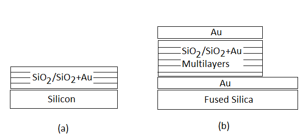 | Figure 1. Cross Sectional Deposition Geometry of 100 alternating SiO2/SiO2+Au nano-layers on (a) silicon (Si) and (b) fused silica (suprasil) substrate |
3. Results and Discussion
- Figure 1 shows the cross-sectional deposition geometry of 100 alternating SiO2/SiO2+Au nano-layers on (a) silicon (Si) and (b) fused silica (suprasil) substrate. The sample geometry given in figure 1(a) is for van der Pauw, SEM, and optical measurements; 1(b) is for Seebeck coefficient measurements.Figure 2 shows the temperature dependence of Seebeck coefficients of 100 multilayers of SiO2/SiO2+Au thin films annealed at the different temperatures. As seen from figure 2, the Seebeck coefficient increased in the negative direction when they were annealed at suitable temperatures. When the annealed samples were measured for their Seebeck coefficient depending on temperatures change, the increase in Seebeck coefficient in negative direction was recorded for the samples annealed at 400°C and 500°C. The Seebeck coefficient reached its highest value for the sample annealed at 500°C when the measured temperature reached 360 K. As seen from figure 2, the highest Seebeck coefficient was recorded as about -425 µV/K at 360 K. The increase in Seebeck coefficient is one of the expected parameters for the high efficient thermoelectric materials and devices. We did similar studies on the same multilayer systems before and, we reached the Seebeck coefficient of about -60 µV/K at 360 K for 50 multilayers at the thickness of 500 nm [1], and the Seebeck coefficient of about -50 µV/K at 360 K for 50 multilayers at the thickness of 147 nm [14]. Our reaching here the much higher Seebeck coefficient might arise from a) the number of multilayers was doubled, and b) the total thickness of the multilayer thin films was higher than the doubles of the sample in ref. [1] and eight times thicker than the sample in ref. [14]. The previous two studies have been modified to form nano-clusters and/or nano-dots in the multilayers using high-energy ion bombardment, but the current study has been performed under the different temperatures for annealing to form nano-dots and/or nano-clusters in the multilayers. It seems that the chosen annealing temperatures and the films thickness for the current study have better effects on the multilayer thin film systems than the high energy beam at the previous selected fluences. Both temperature annealing and ion beam bombardment cause the similar effects on the Seebeck coefficient of the multilayered thin film systems.
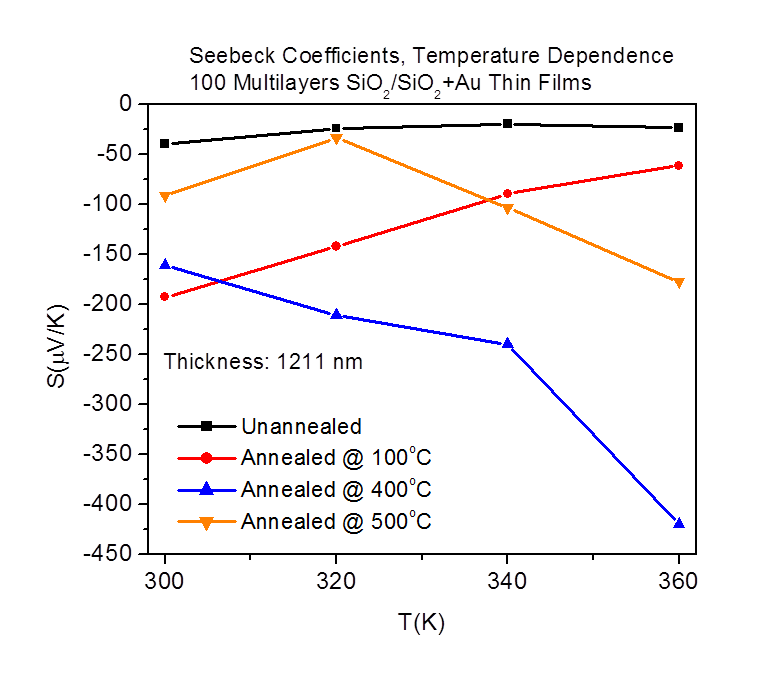 | Figure 2. Temperature Dependence of Seebeck Coefficients of 100 Multilayers of SiO2/SiO2+Au Thin Films Annealed at the Different Temperatures |
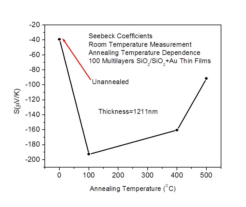 | Figure 3. Annealing Temperature Dependence of Seebeck Coefficients Measured at Room Temperature of 100 Multilayers of SiO2/SiO2+Au Thin Films |
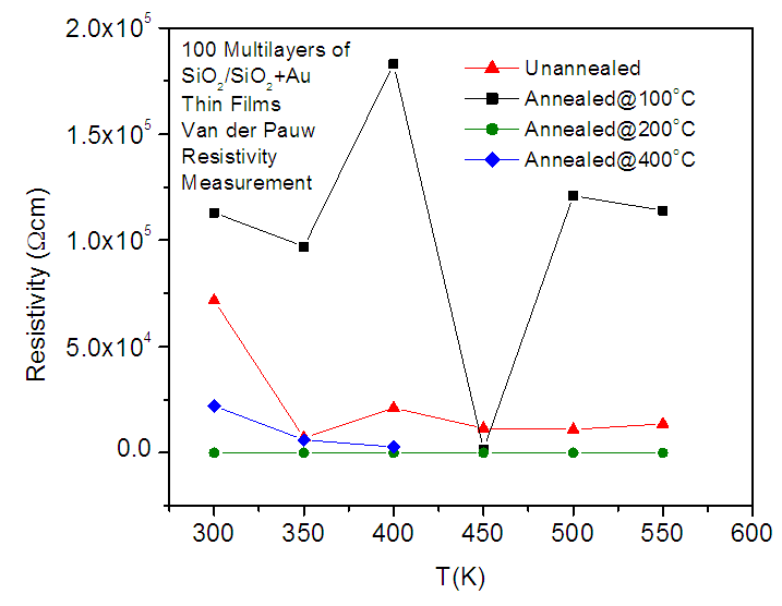 | Figure 4. Temperature Dependence of van der Pauw Resistivity Values of 100 Multilayers of SiO2/SiO2+Au Thin Films Annealed at the Different Temperatures |
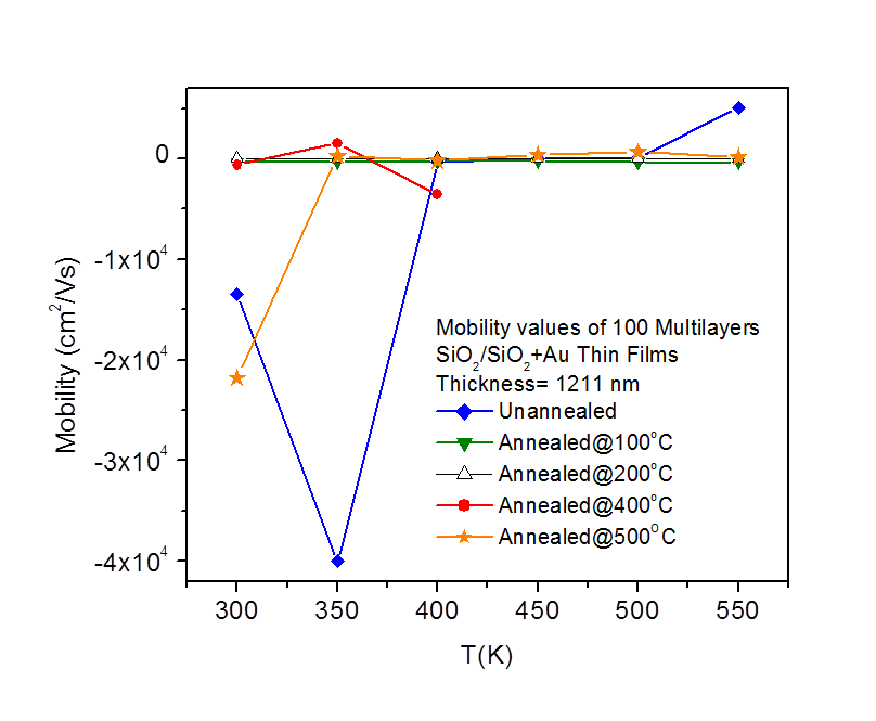 | Figure 5. Temperature Dependence of Mobility Values of 100 Multilayers of SiO2/SiO2+Au Thin Films Annealed at the Different Temperatures |
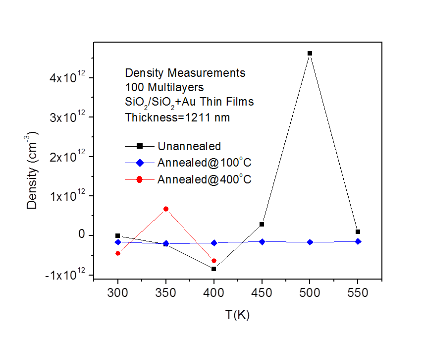 | Figure 6. Temperature Dependence of Density Values of 100 Multilayers of SiO2/SiO2+Au Thin Films Annealed at the Different Temperatures |
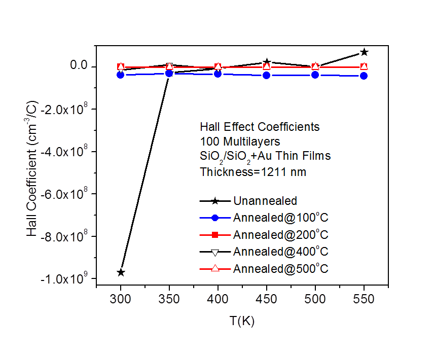 | Figure 7. Temperature Dependence of Hall Coefficients of 100 Multilayers of SiO2/SiO2+Au Thin Films Annealed at the Different Temperatures |
 | (1) |
 : electron velocity corresponding to the Fermi energy of the metal (
 =1.39×108 cm s-1 for gold) and
 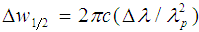 , where
  is the full width at half maximum (FWHM) wavelength and
  is the peak wavelength both determined from an optical absorption spectrum.
  depends on the element implanted and
  is related to the size of the nano-clusters [11].
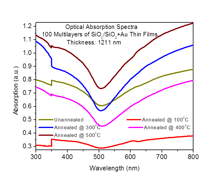 | Figure 8. Optical Absorption Spectra of 100 Multilayers of SiO2/SiO2+Au Thin Films Annealed at the Different Temperatures |
 | Figure 9. SEM+EDS Analysis of Unannealed 100 Multilayers of SiO2/SiO2+Au Thin Film |
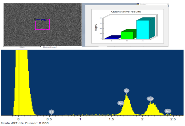
 | Figure 10. SEM Mapping Analysis of Unannealed 100 Multilayers of SiO2/SiO2+Au Thin Film |
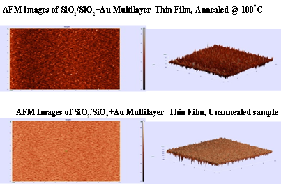 | Figure 11. AFM Images of 100 Multilayers of SiO2/SiO2+Au Thin Films for Unannealed and Annealed at 100°C |
4. Conclusions
- In this study we reported on the preparation of the thermoelectric thin films with the 100 alternating SiO2/SiO2+Au nano-layers, thermal annealing effects on the fabricated thermoelectric thin film systems and their characterizations with Seebeck coefficient measurement, van der Pauw resistivity measurement, mobility, density, Hall Effect measurements, Optical absorption spectroscopy, Scanning Electron Microscopy (SEM) and Energy Dispersive Spectroscopy (EDS) analysis, and Atomic Force Microscopy (AFM). The Seebeck coefficient reached its highest value for the sample annealed at 500°C when the measured temperature reached 360 K. The highest Seebeck coefficient was recorded as about -425 µV/K at 360 K. The resistivity values increased when it was annealed at 100°C, and then decreased and reached the lowest value when the annealing temperature reached the 200°C. Temperature annealing affected the negative mobility and Hall Effect coefficients to shift to the positive direction. The optical absorption spectra got narrower when the annealing temperatures increased. SEM shows that the surface of the multilayer thin films is very smooth. We are planning more detailed temperature range for the characterizations to see more effective and accurate results.
ACKNOWLEDGEMENTS
- Research sponsored by Materials Research Laboratory (MRL), National Science Foundation under NSF-EPSCOR R-II-3 Grant No. EPS-1158862, DOD under Nanotechnology Infrastructure Development for Education and Research through the Army Research Office # W911 NF-08-1-0425, and DOD Army Research Office # W911 NF-12-1-0063, U.S. Department of Energy National Nuclear Security Admin with grant# DE-NA0001896 and grant# DE-NA0002687, NSF-REU with Award#1156137.