Stephen U. Egarievwe1, 2, 3, Julius O. Jow1, 2, Alexander A. Egarievwe2, Rubi Gul2, 3, Richard D. Martin2, Zaveon M. Hales2, Anwar Hossain3, Utpal N. Roy3, Ralph B. James3
1Department of Electrical Engineering and Computer Science, Alabama A&M University, Normal, USA
2Nuclear Engineering and Radiological Science Center, Alabama A&M University, Normal, USA
3Nonproliferation and National Security Department, Brookhaven National Laboratory, Upton, USA
Correspondence to: Stephen U. Egarievwe, Department of Electrical Engineering and Computer Science, Alabama A&M University, Normal, USA.
| Email: |  |
Copyright © 2015 Scientific & Academic Publishing. All Rights Reserved.
Abstract
Chemical etching and chemo-mechanical polishing are techniques used to remove surface defects and damages caused by cutting and mechanical polishing of cadmium zinc telluride (CdZnTe) nuclear detector materials. Etching and chemo-mechanical polishing processes often form thin films on the surfaces of the CdZnTe wafers. While several studies have been done on etching and chemo-mechanical polishing using different chemicals, there is a lack of reporting on the uses of the same chemical solution to study the effects of these two-surface processing techniques. This paper focuses on comparing the effects of chemical etching and chemo-mechanical polishing on the electrical properties of CdZnTe detectors using the same chemical solution: bromine-methanol-ethylene glycol. Three CdZnTe samples were cut from the same region of the ingot, mechanically polished, and used to studying the two surface processing techniques. The current-voltage experiments on the samples gave a measured bulk resistivity of 2.6 x 10¹⁰ Ω-cm for mechanical polishing, 1.6 x 10¹⁰ Ω-cm for chemical etching, and 3.5 x 10¹⁰ Ω-cm for chemo-mechanical polishing. The variations in the measured resistivity for the different surface processing techniques are due to the additional contribution of surface currents to the measured bulk current. The spectral response measurements of the 59.5-keV peak of Am-241 gave a full-width-at-half-maximum (FWHM) of 30.4%, 20.7%, and 30.8% for the mechanical polishing, chemical etching, and chemo-mechanical polishing respectively. In this study, the chemo-mechanical polishing process resulted in a lower measured bulk current. The chemical etching process gave a better spectral resolution (FWHM = 20.7%), and a higher charge-carrier mobility–lifetime product of 0.86 x 10⁻³ cm2/V compared to 0.62 x 10⁻³ cm2/V and 0.64 x 10⁻³ cm2/V for mechanical and chemo-mechanical polishing processes respectively.
Keywords:
Cadmium zinc telluride detector, Chemical etching, Chemo-Mechanical polishing, Surface defects
Cite this paper: Stephen U. Egarievwe, Julius O. Jow, Alexander A. Egarievwe, Rubi Gul, Richard D. Martin, Zaveon M. Hales, Anwar Hossain, Utpal N. Roy, Ralph B. James, Effects of Etching and Chemo-Mechanical Polishing on the Electrical Properties of CdZnTe Nuclear Detectors, American Journal of Materials Science, Vol. 5 No. 3A, 2015, pp. 16-20. doi: 10.5923/s.materials.201502.03.
1. Introduction
Cadmium zinc telluride (CdZnTe) has found applications in X-rays and gamma-rays detection in medical imaging [1, 2], astrophysics [2], and national security. The CdZnTe detector device fabrication involved cutting wafers of desired sizes from the crystal ingot, followed by polishing, surface treatment, and deposition of electrical contacts. During the cutting of wafers from the CdZnTe ingot, defects are induced on the surfaces. Rough surfaces increase leakage current and create charge-carrier trapping centres that limit the performance of CdZnTe detectors [3, 4]. The CdZnTe wafers are mechanically polished to produce very smooth surfaces. Further smoothening is accomplished through etching of the surfaces by dipping in about 1% to 2% bromine methanol solution before contacts are deposited on two opposite planner surfaces. In previous experiments, our atomic force microscopy (AFM) results showed that the surface-area roughness of the CdZnTe wafer was reduced from 9.25 nm root mean square (RMS) for mechanical polishing, to 2.50 nm RMS after etching in 2% bromine-methanol solution [5]. The chemical etching of CdZnTe wafers has been reported to result in a Te-rich surface layer that is subject to oxidation [3-7]. The chemical etching process using bromine-methanol solution has also been observed to increase the surface leakage current [3], which in turn, adds to the measured bulk current. The bromine-methanol solution induces surface features that make them more conductive [3]. We have reported improvements through the usage of a bromine-based passivated etchant where the residual Br is removed from the surfaces to generate nonconductive smooth surfaces, and the use of non-bromine-based etchants for treating the polished surfaces [8]. We also replaced the chemical etching in bromine-methanol solution with chemo-mechanical polishing using hydrogen bromide in hydrogen peroxide solution, and also using bromine methanol ethylene glycol solution [9, 10]. The etching and chemo-mechanical polishing processes often form thin films on the surfaces of the CdZnTe wafers. The properties of the thin films influence the amount of surface current that is added to the measured bulk current. Extensive research has been done on etching and chemo-mechanical polishing using different chemicals [3-10], but there is a lack of reporting on the uses of the same chemical solution to study the effects of these two surface-processing techniques. This paper focuses on comparing the effects of chemical etching and chemo-mechanical polishing on the electrical properties of CdZnTe detectors using the same chemical solution: bromine-methanol-ethylene glycol.
2. Experimental Procedure
Three CdZnTe samples (1, 2, and 3), each sized 6 x 6 x 2 mm3, were cut from the same wafer of the bulk ingot. The three samples (samples 1, 2, and 3) were mechanically polished with 800-grit and 1200-grit silicon carbide abrasive papers, followed by polishing on MultiTex pads with decreasing size alumina powder to 0.9 µm. Sample 1 was used as the control, sample 2 was chemically etched in bromine-methanol-ethylene (BME) glycol solution, and sample 3 was chemo-mechanically polished in BME glycol solution. The chemical etching was done by dipping and slowly moving the CdZnTe sample in the BME glycol solution in a circular motion for about 2 minutes. The chemo-mechanical polishing was accomplished by polishing the wafer on felt pad using BME glycol solution. The chemo-mechanical polishing time for each surface of the wafer was about 1 minute.To enable current–voltage (I–V) measurements, gold contacts were deposited on the two opposite planner surfaces of each CdZnTe sample. This was accomplished by using a pipette to put an appropriate size drop of 5% gold chloride solution on the planner surface. The I–V measurements were made using a customized current-voltage probe in a metal box that is connected to a Keithley Picoammeter/Voltage Source.After the I–V measurements, we recorded the spectral responses of the three samples for Am-241 gamma line at an applied voltage of 150 V. The set-up consists of a standard eV Products’ brass holder used to secure the detector against a beryllium window with a gold-plated spring contact. The brass holder was connected to a multi-channel analyser (MCA) through a pre-amplifier and a shaping amplifier. Each CdZnTe detector was irradiated with a sealed Am-241 gamma-ray source, and the generated signal was recorded through the MCA and stored for processing and analysis.
3. Results and Discussion
The I–V curves for the surface processing techniques are shown in Figures 1–3. We expect the electrical properties and spectral responses of the three samples to be similar since they were cut from the same wafer of the CdZnTe ingot. Any difference in these electrical properties and spectral responses would be due to the surface processing techniques and the electrical contacts. The measured bulk leakage currents include contributions from surface currents.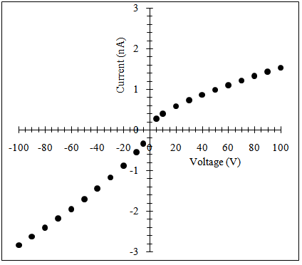 | Figure 1. I-V plot of the CdZnTe sample 1: Mechanical polishing only |
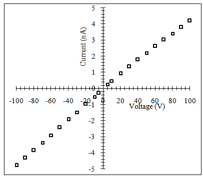 | Figure 2. I-V plot of the CdZnTe sample 2: Mechanical polishing followed by chemical etching. The curve showed a perfect ohmic contact, but an increase in the measured current compared to Figure 1 |
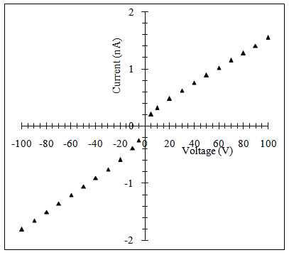 | Figure 3. I-V plot of the CdZnTe sample 2: Mechanical polishing followed by chemo-mechanical polishing. The curve showed a decrease in the measured current compared to Figure 1, and contrary to Figure 2 where chemical etching increased the current |
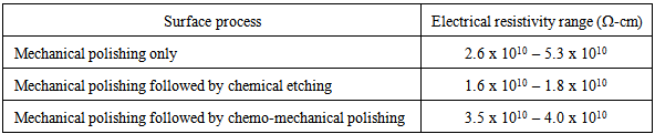
The I–V curve for the mechanical polishing followed by chemical etching (Figure 2) showed a perfect ohmic contact, but it resulted in an increased measured current compared to that of the control sample (Figure 1). In contrast, the mechanical polishing followed by chemo-mechanical polishing gave a near-ohmic contact I–V (Figure 3), and a decrease in the measured current compared to the control sample (Figure 1). The electrical resistivity range for each sample is shown in Table 1 for both positive and negative applied voltage.Table 1. Electrical resistivity for the CdZnTe samples as calculated from current-voltage measurements
 |
| |
|
On the average (using positive and negative applied voltages), the chemical etching process increased the measured electrical resistivity while further increase was measured for the chemo-mechanical polishing process, as well. The variations in the measured resistivity for the different surface processing techniques are due to the additional contribution of surface currents to the measured bulk current.Figures 4 – 6 show the spectral responses of the CdZnTe samples to irradiation with a sealed Am-241 gamma-ray source for the three surface processing techniques. The applied bias is 150 V, and the shaping time is 1 µs for all three samples. The full-width-at-half-maximum (FWHM) for the 59.5–keV energy peak of Am-241 is 30.4% for the mechanical polishing only, 20.7% for chemical etching, and 30.8% for chemo-mechanical polishing. Thus, the chemical etching gave a better spectral resolution. The 59.5–keV energy peak remained stable at about the same channel number for the three surface processing techniques.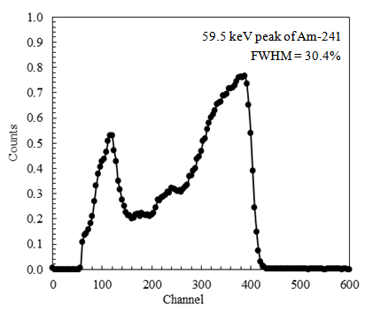 | Figure 4. The spectral response of mechanically polished CdZnTe sample using a sealed Am-241 source |
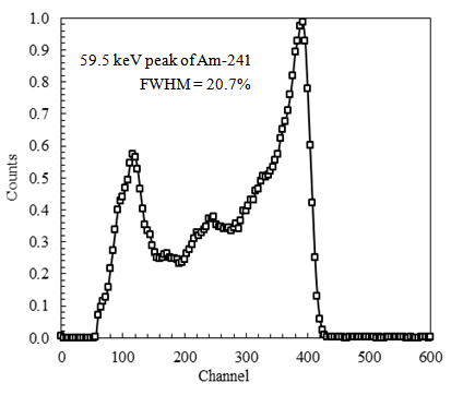 | Figure 5. The spectral response of CdZnTe sample mechanically polished followed by chemical etching in bromine-methanol-ethylene glycol solution. The energy resolution is improved to 20.7% from 30.4% in Figure 1 |
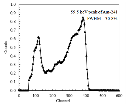 | Figure 6. The spectral response of CdZnTe sample mechanically polished followed by chemo-mechanical polishing with bromine-methanol-ethylene glycol solution. There is no significant change in energy resolution compared to Figure 1 |
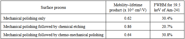
The mobility–lifetime product,  was extracted using the Hecht equation [11], from the best fit of the pulse height of the 59.5–keV gamma peaks taken at different bias voltages; see Figures 7 – 9. As shown in Table 2, the mobility–lifetime product values are in good agreement with the energy resolution of the 59.5 keV peak of Am-241. The best energy resolution (smallest FWHM) corresponds to the highest charge carrier mobility–lifetime product. The value of
  is 0.62 x 10⁻³ cm2/V for the mechanical polishing only, 0.86 x 10⁻³ cm2/V for chemical etching, and 0.64 x 10⁻³ cm2/V for chemo-mechanical polishing. This showed that the sample that is chemically etched has a better mobility– the lifetime product for charge carriers.
Table 2. Energy resolutions (measured as FWHM) and charge carriers’ mobility–lifetime products of the CdZnTe samples
 |
| |
|
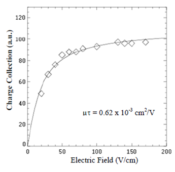 | Figure 7. The mobility–lifetime product of the mechanically polished CdZnTe detector is about  , as extracted from the best fit of the pulse height to the applied voltage using the Hecht equation [11] , as extracted from the best fit of the pulse height to the applied voltage using the Hecht equation [11] |
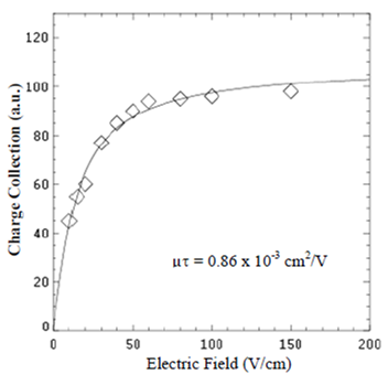 | Figure 8. The mobility–lifetime product of the chemically etched CdZnTe detector is about  , as extracted from the best fit of the pulse height to the applied voltage using the Hecht equation [11] , as extracted from the best fit of the pulse height to the applied voltage using the Hecht equation [11] |
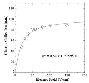 | Figure 9. The mobility–lifetime product of the chemo-mechanically polished CdZnTe detector is about  , as extracted from the best fit using the Hecht equation [11] , as extracted from the best fit using the Hecht equation [11] |
4. Conclusions
We compared the effects of chemical etching and chemo-mechanical polishing on the electrical properties of CdZnTe detectors using the same chemical solution, bromine-methanol-ethylene glycol. The three CdZnTe samples used in this study were cut from the same region of the ingot. Therefore, their electrical properties and spectral responses should be similar, and the recorded differences are mainly due to the surface processing techniques and the electrical contacts. Distinctive results for the current-voltage measurements were obtained with a negative applied voltage, which showed that the chemical etching technique increased the leakage current (bulk plus surface contributions) immediately after the process. In contrast, the chemo-mechanical polishing process decreased the leakage current. These results were further confirmed, for negative applied voltage, by the measured bulk resistivity of 2.6 x 10¹⁰ Ω-cm for mechanical polishing, 1.6 x 10¹⁰ Ω-cm for chemical etching, and 3.5 x 10¹⁰ Ω-cm for chemo-mechanical polishing. The spectral response measurements of the 59.5-keV peak of Am-241 showed the best energy resolution for the chemical etching process, which has a FWHM value of 20.7%, compared to 30.4% for mechanical polishing and 30.8% for chemo-mechanical polishing.The chemical etching process also exhibited the best charge transport properties, with the best mobility–lifetime product of 0.86 x 10⁻³ cm2/V, compared to 0.62 x 10⁻³ cm2/V for mechanical polishing and 0.64 x 10⁻³ cm2/V for chemo-mechanical polishing. The 59.5–keV energy peak remained fairly stable at about the same channel number for the three surface processing techniques.
ACKNOWLEDGEMENTS
This work has been supported by the U.S. Department of Homeland Security, Domestic Nuclear Detection Office, under award number 2012-DN-077-ARI065-04. Alabama A&M University researchers were also supported by the U.S. Nuclear Regulatory Commission through award number NRC-27-10-514, and BNL scientists received support from the U.S. Department of Energy Office of Defense Nuclear Nonproliferation R&D.
References
| [1] | L. Verger, M. Boitel, M. C. Gentet, R. Hamelin, C. Mestais, F. Mongellaz, J. Rustique, and G. Sanchez, “Characterization of CdTe and CdZnTe detectors for gamma-ray imaging applications,” Nucl. Instrum. Methods Phys. Res. A., vol. 458, no. 1-2, pp. 297–309, 2001. |
| [2] | Stefano Del Sordo, Leonardo Abbene, Ezio Caroli, Anna Maria Mancini, Andrea Zappettini and Pietro Ubertini, “Progress in the development of CdTe and CdZnTe semiconductor radiation detectors for astrophysical and medical applications,” Sensors, vol. 9, pp. 3491–3526, 2009. |
| [3] | M. C. Duff, D. B. Hunter, A. Burger, M. Groza, V. Buliga, and D. R. Black, “Effect of surface preparation technique on the radiation detector performance of CdZnTe,” Applied Surface Science vol. 254, pp. 2889–2892, 2008. |
| [4] | A. Hossain, A. E. Bolotnikov, G. S. Camarda, Y. Cui, S. Babalola, A. Burger, and R. B. James, “Effects of surface processing on the response of CZT gamma detectors: studies with a collimated synchrotron X-ray beam,” Journal of Electronic Materials, vol. 38, no. 9, pp. 1356–1361, 2008. |
| [5] | A. Hossain, S. Babalola, A. E. Bolotnikov, G. S. Camarda, Y. Cui, G. Yang, M. Guo, D. Kochanowska, A. Mycielski, A. Burger and R. B. James, “Effect of chemical etching on the surface roughness of CdZnTe and CdMnTe gamma radiation detectors,” Proc. of SPIE 7079, 70791E-1, 2008. |
| [6] | K. Chattopadhyay, M. Hayes, J. O. Ndap, A. Burger, M. J. Lu, H. G. McWhinney, T. Grady and R. B. James, “Surface passivation of cadmium zinc telluride radiation detectors by potassium hydroxide solution,” Journal of Electronic Materials, vol. 29, No. 6, pp. 708–712, 2000. |
| [7] | G. Zha, W. Jie, T. Tan, P. Li, “The surface leakage currents of CdZnTe wafers,” Applied Surface Science, vol. 253, pp. 3476–3479, 2007. |
| [8] | A. Hossain, A. E. Bolotnikov, G. S. Camarda, Y. Cui, D. Jones, J. Hall, K. H. Kim, J. Mwathi, X. Tong, G. Yang and R. B. James, “Novel approach to surface processing for improving the efficiency of CdZnTe detectors,” Journal of Electronic Materials, vol. 43, No. 8, pp. 2771–2777, 2014. |
| [9] | D. E. Jones, S. U. Egarievwe, A. Hossain, I. O. Okwechime, M. L. Drabo, J. Hall, A. L. Adams, S. O. Babalola, G. S. Camarda, A. E. Bolotnikov, W. Chan and R. B. James, “Study of Surface Passivation and Contact Deposition Techniques in CdZnTe X-Ray and Gamma-Ray Detectors,” IEEE Records of Nuclear Science Symposium and Medical Imaging Conference, pp. 4124–4127, 2012. |
| [10] | I. O. Okwechime, S. U. Egarievwe, A. Hossain, Z. M Hales, A. A. Egarievwe and R. B. James, “Chemical treatment of CdZnTe radiation detectors using hydrogen bromide and ammonium-based solutions,” Proc. SPIE 9213, 92130Y, 2014. |
| [11] | K. Hecht, “Zum Mechanismus des lichtelektrischen Primärstromes in isolierenden Kristallen,” Z. Phys., vol. 77, pp. 235–245, 1932. |
 Abstract
 Reference
 Full-Text PDF
 Full-text HTML