| [1] | W. A. Maryniak, T. Uehara, and M. A. Noras, “Surface resistivity and surface resistance measurements using a concentric ring probe technique,” Trek Application Note, 0623/MAN Rev. 1b (1005), 2003. |
| [2] | F. C. Chiu and C. M. Lai, “Optical and electrical characterization of cerium oxide thin films,” Journal of Physics D, vol. 43, no. 7, Article ID 075104, 5 pages, 2010. |
| [3] | D. J. Griffiths, Introduction to Electrodynamics, Prentice Hall, 3th ed., 1999. |
| [4] | L. N. Charyulu, Annapurna Das, and Sisir K. Das, “Analysis and Measurement of crosstalk in printed circuit board due to RF and transient pulses,” in Proc. INCEMIC, 2003, paper, pp. 257-260. |
| [5] | J. F. Nye, Physical Properties of Crystals, Oxford Science Publications, 1985. |
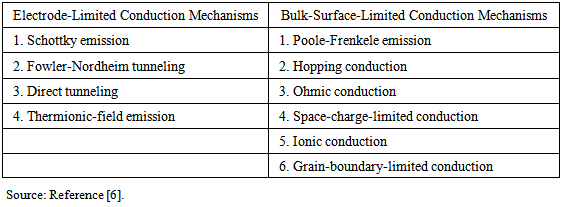
| [6] | Fu-Chien Chiu, “A review on conduction mechanisms in dielectric films,” Advances in Materials Science and Engineering, Hindawi Publishing Corporation, Article ID 578168, pp. 1-18, 2014. |
| [7] | H. Akinaga and H. Shima, “Resistive random access memory (ReRAM) based on metal oxides,” Proceedings of the IEEE, vol. 98, no. 12, pp. 2237-2251, 2010. |
| [8] | Q. Li, Q. Z. Xue, X. L. Gao, and Q. B. Zheng, “Temperature dependence of the electrical properties of the carbon nanotube/polymer composites,” eXPRESS Polymer Letters, 3(12), pp. 769-777, 2009. |
| [9] | C. K. Wong, and F. G. Shin, “Electrical conductivity enhanced dielectric and piezoelectric properties of ferroelectric 0-3 composites,” J. Appl. Phys., 97, 064111, 2005. |
| [10] | J. Borch, M. Lyne, R. Mark, and C. Habeger Jr., Handbook of Physical testing of Paper, CRC Press, vol. 2(2), 2010. |
| [11] | C. Kittel, Introduction to Solid State Physics, John Wiley and Sons, Hoboken. 8th ed., 2005. |
| [12] | Matthew Edwards, Padmaja Guggilla, John C. Corda, and Stephen Egarievwe, “Measurement of the dielectric, conductance, and pyroelectric properties of MWCNT:PVDF nanocomposite thin films for application in infrared technologies,” SPIE Vol. 8868, no. 11, 2013. |
| [13] | Matthew Edwards, Stephen Egarievwe, Tatiana Kukhtarev, and Jemilia Polius, “Surface resistivity temperature dependence measures of commercial, multiwall carbon nanotubes (MWCNT), or silver nano-particle doped polyvinylidene difluoride (PVDF) and polyvinyl alcohol (PVA) films,” SPIE Vol. 9220, 922009, 2014. |
| [14] | Matthew Edwards, Stephen Egarievwe, Afef Janen, Tatiana Kukhtarev, Jemilia Polius, and John Corda, “Temperature Dependent Surface Resistivity Measures Of Commercial, Multiwall Carbon Nanotubes (MWCNT), and Silver Nano-Particle Doped Polyvinyl Alcohol (PVA) Films,” Materials Sciences and Application Journal, Vol. 5, pp. 915-922, 2014. |
| [15] | A. K. Batra, M. E. Edwards, P. Guggilla, M. D. Aggarwal, and R. B. Lal, “Pyroelectric Properties of PVDF: MWCNT Nanocomposite Film for Uncooled Infrared Detectors and Medical Applications”, Integrated Ferroelectrics, Vol. 158, Iss.1, 2014. |
| [16] | E. Y. Malikov, M. B. Muradov, O. H. Akperov, G. M. Eyvazova, R. Puskas, L. Madarasz, A. Kukovecz, and Z. Konya, “Synthesis and characterization of polyvinyl alcohol based multiwalled carbon nanotube nanocomposites,” Physica E., 61, pp. 129-134, 2014. |
| [17] | Jacob N. Israelachili, Intermolecular and Surface Forces, with applications to colloidal and biological systems, Academic Press, 1985. |
| [18] | Murray R. Spiegel and John Liu, Mathematical Handbook of Formulas and tables, 2nd. Ed., Schaum’s Outlines, McGraw-Hill, New York, NY, 1999. |
| [19] | Chem-Fax, Flinn Scientific, INC., Publication No. 608.00, (2010). |
| [20] | M. M. Elkholy and L. M. Sharaf, “Effect of P2O5 on Microstructure and Properties of Calcium Aluminoborosilicate Glasses,” Mater. Chem. Phys. vol. 65, no. 192, 2000. |
| [21] | Sreelalitha Kramadhati and K. Thyagarajan “Optical Properties of Pure and Doped (KNO3 & MgCl2) Polyvinyl Alcohol Polymer Thin Films,” International Journal of Engineering Research and Development, vol. 6, issue 8, pp. 15-18, 2013. |
| [22] | K. Lang, S. Sourirajan, T. Matsuura, and G. Chowdhury, “A study on the preparation of polyvinyl alcohol thin-film composite membranes and reverse osmosis testing,” Desalination, vol. 104, issue 3, pp 185-196, May 1996. |
| [23] | John Reitz, Frederick Milford and Robert Christy, Foundations of Electromagnetic Theory, 3rd Edition Addison-Wesley Publishers, 1980. |
| [24] | Vikram S. Yadav, Devendra K. Sahu, Yashpal Singh, and D.C. Dhubkarya, “The Effect of Frequency and Temperature in Dielectric Properties of Pure Poly Vinylidene Fluoride (PVDF) Thin Films,” Proceedings of the International Multi-Conference of Engineers and Computer Scientists 2010 Vol III, IMECS 2010, March 17-19, 2010, Hong Kong. |
| [25] | Matthew Edwards, Padmaja Guggilla, John C. Corda, and Stephen Egarievwe, “Measurement of the dielectric, conductance, and pyroelectric properties of MWCNT:PVDF nanocomposite thin films for application in infrared technologies”, SPIE Vol. 8868, no. 11, 2013. |
 Abstract
 Reference
 Full-Text PDF
 Full-text HTML


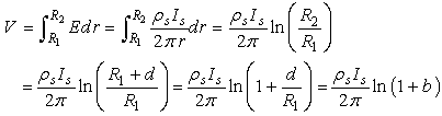
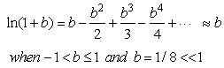
 Since b << 1 [18]