S. Akcaglar 1, S. Akdurak 2, M. Bayburt 2, C. Celiktas 3
1Dokuz Eylul University, Faculty of Engineering, Mechanical Engineering Department, 35100, Bornova, Izmir, Turkey
2Ege University, Institute of Nuclear Sciences, 35100, Bornova, Izmir, Turkey
3Ege University, Faculty of Science, Physics Department, 35100, Bornova, Izmir, Turkey
Correspondence to: M. Bayburt , Ege University, Institute of Nuclear Sciences, 35100, Bornova, Izmir, Turkey.
| Email: |  |
Copyright © 2014 Scientific & Academic Publishing. All Rights Reserved.
Abstract
In this work, a nuclear spectroscopy amplifier was developed to construct a smaller and cheaper an electronic device with low electronic noise, fast rise and fall times, insensitive to overload and temperature degradation, operation at hight count rates, maximum performance according to commercial nuclear amplifiers and without using any NIM module. The developed amplifier shaped the pulses coming from the detector via preamplifier in a suitable form. Semi-Gaussian pulses, which have time constant of 2 μs, were obtained from the output of the amplifier. It operated with the voltage of ±15 V and the current of ±40 mA. The noise reflected to its input was lower than 4μV (eff.). It accepted the pulses with unipolar and bipolar shapes through the coaxial cables of 50, 75 or 93 ohms by decreasing the output impedance, and it had a maximum gain level of 1,280. With these specifications, it was believed that anyone could construct this type nuclear amplifier with low cost and ease. The results obtained from the amplifier were compared with the results of the amplifiers available commercially. They were highly compatible with the results from the commercial ones.
Keywords:
Nuclear spectroscopy amplifier, Low noise, High resolution, Low output impedance, Eurocrate standard module, High Amplification
Cite this paper: S. Akcaglar , S. Akdurak , M. Bayburt , C. Celiktas , Development of an Amplifier for Nuclear Spectrometers, Science and Technology, Vol. 4 No. 3, 2014, pp. 31-41. doi: 10.5923/j.scit.20140403.01.
1. Introduction
The amplifiers used in nuclear spectrometers amplify and shape the signals coming from the detectors in order to process them. They are subdivided into two groups as preamplifiers and main amplifiers. Pulse amplitudes produced by different types of detectors are rather low in µV or mV levels. To process these weak pulses, their amplitudes should be amplified, and they should be shaped for the optimization of their noises, as well. This explains the reason for the necessity of the main amplifiers [1] [2].The functions of a main nuclear amplifier can be examined in detail as follows:
1.1. Time Limitation and Pole-Zero Cancellation
Since the radioactive emitting is random in time, the pulses from the detector are random, and their amplitudes are proportional to the energies of the incident particles. Because the pulse bombardment from the detector causes the pile-up, the pulse duration time should be decreased in the main amplifier. Otherwise, the voltage baseline is saturated and it shifts to the outside of the operation region. To prevent this, a differentiator i.e. a pole-zero cancellator is used. By this way, the noise with low frequency can also be prevented [1]. The more pile-up effect, the less resolution of the system is, as is well known [3].
1.2. Shaping
In order to increase the performance of a nuclear spectrometer and to reach high counting rate, shaping is required [4]. In this process, differentiation and integration operation is made for eliminating the noise from the nuclear pulse [5]. The optimization may be performed by several times integration although differentiation is made once [2].
1.3. Gain
Gain is defined as the ratio of the output pulse amplitude to the input pulse amplitude of an amplifier. 1,000-2,000 times voltage amplification is desired for the nuclear amplifiers [6].
1.4. Baseline Restoration
Another problem in the nuclear electronic systems is the correction of the baseline shift. The reason for the baseline shift is the AC couplage usage between each operational division of the amplifier’s circuit during the pulse processing. The distorted part of the pulse is rejected by shortening the duration time (clipping process) via baseline restorer circuits, preventing addition the distorted part to the subsequent pulses. Thus, the pulses whose amplitudes do not distort and are proportional to the particle energies are obtained.The performances of the main amplifiers can be expressed as functions of their maximum amplification values and integral nonlinearities. In addition, the noise reflected to amplifiers’ inputs and the gain variation coefficients versus temperature affect their performances [2].The objective of this study is to develop a linearly and stably operating nuclear spectroscopy amplifier which is capable of modifying the amplitudes of the input pulses to the inputs of the subsequent devices. To perform this, these features were taken into consideration: low intrinsic noise, fast rise and fall times, insensitivity to overload and operation at high count rates.
2. Experimental
The block diagram of the developed amplifier is shown in Fig. 1.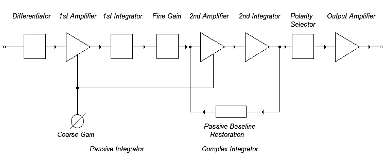 | Figure 1. The block diagram of the developed amplifier |
A pole-zero cancellator as a first differentiator was placed into the input of the amplifier circuit in order to limit the electronic noise affecting the resolution low.The pulses coming from the preamplifier to the amplifier are directly sent to the differentiator circuit in order not to alter the voltage baseline due to pile-up since their duration times are long. Thus, pulse duration times are shortened. The pulses from the preamplifier, as shown in Fig. 2, have generally sharp rising edge and exponential falling edge, and this shape can be express in the following equation;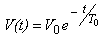 | (1) |
where t, V0, V(t), and T0 are time, input voltage, output voltage and pulse decay time, respectively. 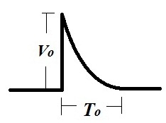 | Figure 2. Preamplifier output shape |
If a pulse is produced by the preamplifier through the detector in this exponential falling edge, its amplitude is added to tail, leading to an increase in mean voltage baseline width [7]. If the amplitudes and the count rates are high, the baseline shifts after a moment and the amplifier does not operate in the linear operation region, and then it saturates. For this reason, it cannot treat the subsequent pulses. To prevent this, pulse duration time should be shortened by passing the pulse through a differentiator circuit [1].The differentiator function is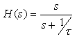 | (2) |
where H(s), s and τ are transfer function, Laplace transform variable and pulse duration time, respectively. From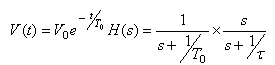 | (3) |
the output voltage is found as 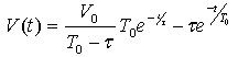 | (4) |
From this equation, it can be stated that the output voltage is limited by the pulse duration time.Most part of the electronic noise produced by the amplifier itself is composed of the noise of the first stage gain levels. The noise of the first level reaches to the output by multiplying all of the gain levels. In the developed amplifier, gain of the first level was made higher than that of the other levels. Thus, the first gain level produces the more noise than the other levels. If, therefore, the noise of the first gain level can be decreased, the most part of the noise can be prevented and the resolution will be increased [8].Operational amplifiers were used in the amplifier circuit owing to their good specifications and low cost. However, it has been determined that the operational amplifiers have high intrinsic noise due to their production technique. To cope with this problem, a dual transistor with low noise was connected to the amplifier circuit so as to eliminate the noise of input transistors of the used operational amplifier. Thus, it was used with its maximum performance, and the noise of the first gain level was minimized.
2.1. Integrator
An integrator (a RC circuit), i.e. low-pass filter circuit, was placed just after the first amplifier block to refine the pulses from noise [9]. In addition, the RC filter circuit was fixed for the best noise optimization.A fine adjustment potentiometer, which works as a voltage divider, was placed into the output of the integrator for changing the gains between x2 and x10 levels.
2.2 Amplification Division
Nuclear amplifiers are produced for amplifying the signals about 1,000-2,000 times [1] [2]. The pulses coming from the preamplifier to the amplifier have amplitudes of 0-100 mV voltage interval. In order to refine these pulses from noise and to deal with them in the electronic devices such as analog to digital converter (ADC), single channel analyzer (SCA), time analyzer and counter, the amplification of the pulses is accomplished by the main amplifiers. Since the rise and fall times of the pulses coming from the integrator were extended, it was decided that the pulses were amplified by a medium rate amplifier. The total gain, thus, was increased.The operational amplifier was used for noninverting connection in this section. The gain was changed by selecting the feedback resistance values with a switch. This was the coarse gain adjustment of the main amplifier.
2.3. Active integrator
An active integrator with operational amplifier was used for pulse shaping and noise amplification. If the gain selection of the active integrator is chosen between 1 and 3, the circuit works as an integrator with complex pole. This circuit without a coil was preferred for its ease application and construction [10].
2.4. Polarity Selector and Last Amplification Division
The pulses coming from the detectors and preamplifiers can have unipolar or bipolar shapes. A polarity inverter switch is required for polarity adaptation of the devices after the main amplifiers. The last amplification division is composed of an operational amplifier. A switch was used for polarity selection. The input signal was sent to the output by inverting or selecting as it is by means of the polarity selector. The amplifier amplified the pulses with different polarity in the same portion.
2.5. Impedance Matching
Output resistances of the existent operational amplifiers are generally high (more than 100 ohm). If we consider that the characteristic impedances of the coaxial cables are 50 and 93 ohms, impedance matching should be applied between the output of the amplifier and the cable for maximum power transfer [11]. This matching was done by connecting two push-pull transistors to the output of the operational amplifier, amplifying the current and decreasing the output impedance.To use and adjust the amplifier easily, a LED (Light Emitting Diode) was mounted to the output together with a small circuit indicating overload. Thus, it could be understood through the LED whether the amplifier was saturated to incoming pulses without using an oscilloscope.
3. Results and Discussion
The characteristics of the developed amplifier are summarized in Table 1.| Table 1. Characteristics of the developed amplifier |
| | Input impedance | ~1 KΩ | | Input amplitude | ±50 V max. | | Amplification | Coarse: 4, 8, 16, 32, 64, 128 gradualFine: x2-x10 continualMaximum amplification: 1280 | | Couplage | DC couplage | | Noise | <4 μV effective (transferred to input) | | Shaping time constant | 2 μs | | Shaping type | Semi-GaussianPassive RC-CRActive integrator | | Polarity | (+) and (-) by switch | | Nonlinearity | 0.12% | | Output amplitude | ±10 V max. | | Output impedance | 50 Ω | | Operation temperature | 0-50 C | | Baseline shift by temperature | 0.94 mV/C max. | | Baseline restorer | 0.2 s passive RC | | Overload relaxation time | 2 μs [12] | | Bias | ±15 V, ±25 mA | | Dimension | 3U Eurocrate module (100x160)mm |
|
|
In order to determine these characteristics, output direct (DC) voltage baseline of a bias supplier was adjusted to 0 V by short circuiting the input of the developed amplifier in maximum amplification. A pulse was fed to input of the amplifier and the amplification of the active integrator was adjusted so as to cause no ringing at the output.
3.1. Amplification
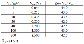
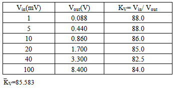
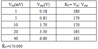
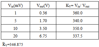
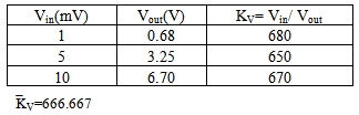
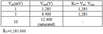
An input pulse from a pulse generator was directed to the input of the developed amplifier, and the output pulse was screened through an oscilloscope. Fine gain switch of the amplifier was adjusted to its maximum level and the coarse gain switch was changed to all amplification levels one by one during this measurement (Bias: ±15 V).Vin, Vout and  quantities in the following tables are input voltage, output voltage and mean value of the gain levels, respectively.
Table 2. First gain level (min.)
 |
| |
|
Table 3. Second gain level
 |
| |
|
Table 4. Third gain level
 |
| |
|
Table 5. Fourth gain level
 |
| |
|
Table 6. Fifth gain level
 |
| |
|
Table 7. Sixth gain level (min.)
 |
| |
|
3.2. Output Pulse Shape
The developed amplifier’s input pulse shape from an Eberline model MP-2 mini pulse generator and its output pulse shape are given in Figs. 3 and 4, respectively. The pulse shape after pole-zero compensation was obtained by enlarging the oscilloscope time scale. In this connection, rise time of the output pulse and total pulse time were obtained as 3.8 μs and 11.8 μs, respectively.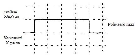 | Figure 3. Input pulse shape |
 | Figure 4. Output pulse shape |
Distribution of the amplification between all divisions was observed, via an oscilloscope, in the selected A, B, C, D, E and F points. This distribution is shown in Table 8.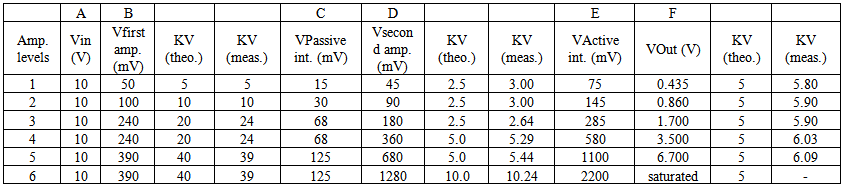 | Table 8. Distribution of the amplification between the divisions |
These A-F points are the points between each amplification division as stated in the previous sections (2.1-2.5) above and are illustrated in Fig. 5.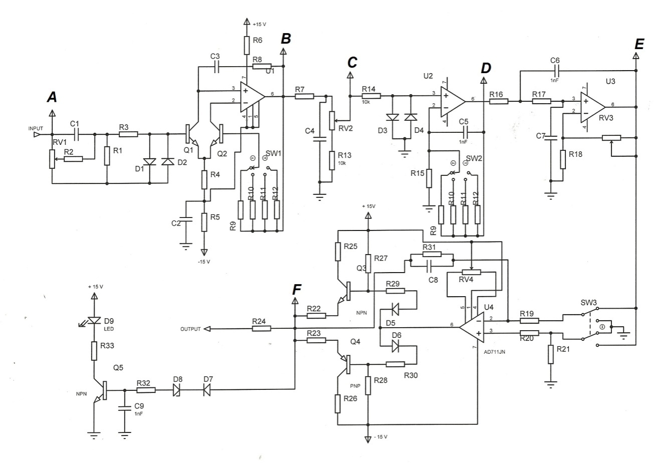 | Figure 5. A-F test points between all amplification divisions |
3.3. Measurement of Noise
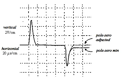
The input of the developed amplifier was grounded via a resistor of 100 ohm and the output noise was measured with an AC milivoltmeter and an oscilloscope. This measurement was performed for whole coarse gain range while fine gain switch was on its maximum level. The input noise results were obtained by dividing the effective voltages to the mean amplification values. Obtained results can be seen in Table 9.Observed signal shapes in J1, J2, J3 and J4 test points of the arrangement in Fig. 7 are illustrated in Fig. 8. | Table 9. Input noise results |
| | Amplification levels | Measured mean amplification | Oscilloscope results (mV) | Effective noise from the input via voltmeter (μV) | Voltmeter results (mV) | Effective noise from the input via oscilloscope (μV) | | 1 | 43.00 | 2 | 7.04 | 0.315 | 7.15 | | 2 | 85.58 | 3 | 5.18 | 0.465 | 5.20 | | 3 | 170.00 | 5 | 4.45 | 0.835 | 4.60 | | 4 | 346.80 | 9 | 3.93 | 1.280 | 3.55 | | 5 | 666.60 | 17 | 3.86 | 2.400 | 3.60 | | 6 | 1282.50 | 32 | 3.70 | 4.500 | 3.50 |
|
|
The linearity measurements for all amplification levels are given in Table 10. These measurements could solely be done until output voltages of 5 V for 1st, 2nd and 3rd amplification levels due to the insufficiency of the pulse generator. The voltage axis of the oscilloscope was adjusted to 10 mV/cm during the measurements.| Table10. Deviations (or Errors) in amplification levels |
| | Vout (V) | 1st Level (mV) | 2nd Level (mV) | 3rd Level (mV) | 4th Level (mV) | 5th Level (mV) | 6th Level (mV) | | 0.5 | 0 | 0 | 0 | 0 | 0 | 0 | | 1.0 | +2.0 | +2.0 | 0 | 0 | 0 | 0 | | 1.5 | +2.0 | +2.0 | +2.0 | 0 | 0 | 0 | | 2.0 | +4.0 | +2.0 | +2.0 | +2.0 | 0 | 0 | | 2.5 | +4.0 | +4.0 | +3.0 | +2.0 | +2.0 | 0 | | 3.0 | +4.0 | +4.0 | +3.0 | +2.0 | +2.0 | +2.0 | | 4.0 | +4.0 | +3.0 | +3.0 | +2.0 | 0 | 0 | | 5.0 | 0 | 0 | 0 | 0 | 0 | 0 | | 6.0 | | | | 0 | 0 | 0 | | 7.0 | | | | 0 | 0 | 0 | | 8.0 | | | | 0 | 0 | 0 | | 9.0 | | | | -2.0 | 0 | 0 | | 10.0 | | | | -3.0 | -2.0 | 0 |
|
|
The noise signal shape observed on the oscilloscope screen is shown in Fig. 6. | Figure 6. Noise signal shape |
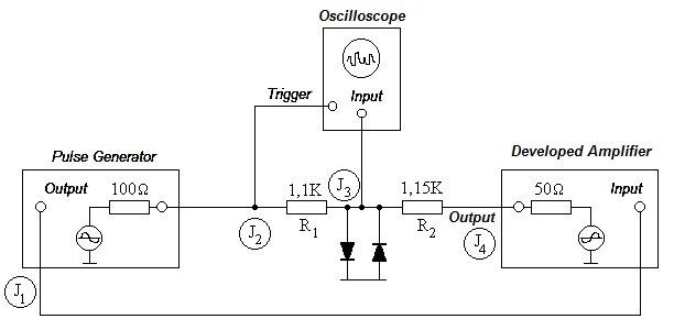 | Figure 7. Linearity measurement arrangement |
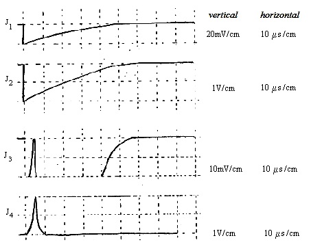 | Figure 8. Observed signal shapes in J1, J2, J3 and J4 test points in Fig. 7 |
3.4. Linearity
Linearity of the developed amplifier was measured via an arrangement composed of a pulse generator (Ortec model 419) and an oscilloscope (Trio 100 MHz model CS-2100). The block diagram of the arrangement can be seen in Fig. 7.
3.5. Overload
The pulses obtained from the pulse generator were directed to the input of the developed amplifier as it was said before. Then, the amplifier was overloaded by amplifying 100 times its input pulses with the amplitudes of 10 V. The fall time of the saturated pulses were determined as shown in Table 11.| Table 11. Fall times of the saturated pulses |
| | Gain Levels | Standard width of the pulse baseline (s) | Pulse baseline width (tp) when overloaded (%10)(s) | | 1 | 14 | 26 | | 2 | 14 | 26 | | 3 | 14 | 26 | | 4 | 14 | 26 | | 5 | 14 | 27 | | 6 | 14 | 29 |
|
|
An explanatory illustration for the pulse baseline width when the amplifier overloaded is shown in Fig.9.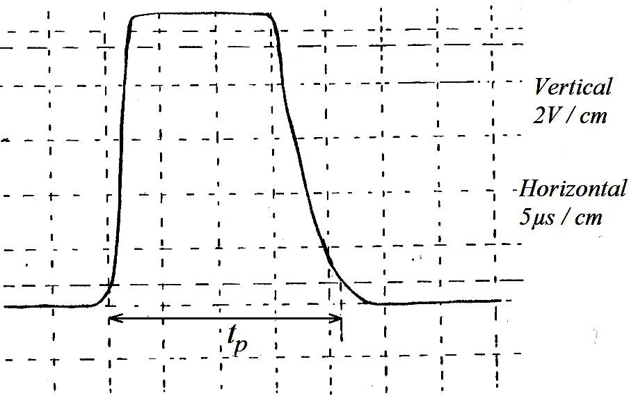 | Figure 9. Pulse baseline width (tp) of the overloaded amplifier |
3.6. Output Charging
The change of the output pulses of the developed amplifier versus charging was studied to check whether a change existed in the amplitude of the pulse. Therefore, the oscilloscope was connected to the point which was in the amplifier side of the impedance matcher resistor of 47 ohm. Also, amplifier output was grounded and the changes for various output voltages were measured as given in Table 12.| Table 12. Output pulses of the developed amplifier versus charging. (Vout: output voltage of the amplifier, V: change in the output voltage) |
| | Vout(V) | 1 | 2 | 3 | 4 | 5 | 6 | 7 | 8 | 9 | 10 | | V(mV) | 11 | 12 | 14 | 13 | 15 | 15 | 15 | 16 | 18 | 20 |
|
|
3.7. Temperature Stability
The amplifier was put into a box and then warm air was blown into the box in order to determine the output baseline shift versus the temperature change by using a digital voltmeter. These changes are given in Table 13.| Table 13. The change on the gain levels |
| | Temperature (C) | 1st Level(mV) | 2nd Level(mV) | 3rd Level(mV) | 4th Level(mV) | 5th Level(mV) | 6th Level(mV) | | 15 | -3.0 | -4.0 | -5.7 | -6.4 | -8.2 | -11.9 | | 20 | -1.8 | -2.1 | -3.6 | -4.3 | -6.6 | -8.4 | | 25 | 0 | 0 | 0 | 0 | 0 | 0 | | 30 | +1.0 | +1.5 | 1.9 | +2.2 | +3.0 | +3.4 | | 35 | +3.9 | +4.5 | +5.9 | +6.3 | +7.1 | +18.3 | | 40 | +4.7 | +6.3 | +6.8 | +7.4 | +9.0 | +19.5 | | 45 | +6.9 | +8.5 | +9.2 | +10.0 | +12.6 | +20.6 | | 50 | +8.4 | +9.7 | +10.5 | +13.2 | +16.4 | +21.0 |
|
|
3.8. Effect of the Bias Voltage Change
Output baseline was observed by altering bias voltages symmetrically in every amplification level as shown in Table 14.| Table 14. Gain levels and baseline shift (mV) |
| | Bias Voltage (V) | 1st Level(mV) | 2nd Level(mV) | 3rd Level(mV) | 4th Level(mV) | 5th Level(mV) | 6th Level(mV) | | 15 | 0 | 0 | 0 | 0 | 0 | 0 | | 14 | -1.9 | -3.8 | -3.5 | -3.6 | -5.2 | -5.9 | | 13 | -4.9 | -7.1 | -7.2 | -8.8 | -13.4 | -13.8 | | 12 | -7.7 | -11.3 | -10.6 | -14.1 | -21.0 | -23.2 | | 11 | -10.7 | -15.6 | -15.3 | -19.1 | -28.8 | -33.1 |
|
|
3.9. Operation with Nuclear Pulses
The operation of the developed amplifier for use in nuclear studies was compared with the operation of Ortec model 451 spectroscopy amplifier. For this purpose, a scintillation detector [NaI(Tl) of 3"x3"] and a 60Co of 10 μCi activity radioactive source were used. The detector output was connected to an Ortec model 113 preamplifier. The preamplifier output was sent to both developed and Ortec model 451 spectroscopy amplifiers, and their outputs were also connected to the channel A and B inputs of the oscilloscope. Pole-zero adjustments of both amplifiers were done. In Fig. 10, the preamplifier output pulses are given.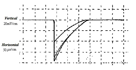 | Figure 10. Preamplifier output pulses |
After adjusting the amplification levels of the amplifiers, their outputs were observed as given Fig. 11.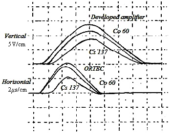 | Figure 11. The output shapes of the amplifiers |
The top and bottom pulse shapes in this figure were obtained from the developed amplifier and Ortec model 451 amplifier, respectively.
4. Conclusions
The characteristics of the developed amplifier in this work were compared with the characteristics of the nuclear amplifiers commercially available as given in Table 15 [13] [14] [15]. In overall comparison in the table, the developed amplifier has quite adequate characteristics as well as the others.| Table 15. Comparison of the amplifiers |
| | Company | Model | Amplification | Time constant (μs) | Linearity (%) | Noise (Veff-μV) | | ORTEC | 672 | 1,500 | 2 | 0.025 | 4.5 | | ORTEC | 671 | 1,500 | 2 | 0.025 | 4.5 | | ORTEC | 575A | 1,250 | 2 | 0.05 | 5 | | ORTEC | 572 | 1,500 | 2 | 0.05 | 5 | | ORTEC | 571 | 1,500 | 2 | 0.05 | 5 | | ORTEC | 451 | 5-2,000 | 0.5-1.20 | 0.050 | 5.0 | | ORTEC | 472 | 2.5-300.0 | 0.25-6.00 | 0.050 | 4.0 | | ORTEC | 432 | 1,600 | 1.00 | 0.075 | 10.0 | | ORTEC | 410 | 0.75-1,300.00 | 0.1-10.0 | 0.100 | 7.0 | | CANBERRA | 2026 | 1,500 | 2 | 0.04 | 4.5 | | CANBERRA | 2022 | 3,600 | 2 | 0.05 | 4 | | CANBERRA | 2015 | 1,280 | 0.50-2.00 | 0.250 | 7.0 | | CANBERRA | 2013 | 3,000 | 0.50-4.00 | 0.500 | 3.5 | | CANBERRA | 2012 | 1,280 | 0.50-2.00 | 0.500 | 7.0 | | CANBERRA | 2011 | 3,000 | 0.50-4.00 | 0.500 | 3.5 | | CANBERRA | 2010 | 3,000 | 0.25-12.00 | 0.500 | 4.0 | | CANBERRA | 1713 | 3,000 | 1-12 | | 4.0 | | CANBERRA | 1413 | 3,000 | 0.50-8.00 | 0.050 | 4.0 | | CANBERRA | 1412 | 3,000 | 0.25-12.00 | 0.010 | 3.5 | | CANBERRA | 1411 | 1,000 | 0.20-1.00 | 0.100 | 10.0 | | CANBERRA | 814 | 600 | 1.20 | 0.500 | 10.0 | | WENZEL | N-LVA 211 | 0.4-1,000.0 | 2.00 | 0.050 | 3.0 | | Developed amplifier | | 1,280 | 2.00 | 0.120 | 4.0 |
|
|
A monolithic dual transistor was placed into the input of the operational amplifier by eliminating its input transistors. Thus, the electronic noise level was degraded, and a high compatible and handy amplifier was constructed. By the help of the overload displayer used in the system, the amplification adjustment could be done easily before the saturation without using an oscilloscope.By placing the polarity chooser switch close to the output division, switching process was performed when the amplitudes of the pulses were high. In this way, possible surrounding noise effects such as electromagnetic effects, room light, temperature etc. were degraded, too.In the above sections, we mentioned the advantages of the amplifier used with totally DC couplage. In this case, temperature change may cause the baseline shift. To prevent this shift, a RC filter circuit with a long time constant was used. By means of this circuit, the pile-up effect owing to the amplifier with DC couplage was prevented.The reason why a baseline correction circuit was not used in the developed amplifier was the fact that these types of circuits are highly noisy and they need to be adjusted according to the radiation count rate. Therefore, a simple RC circuit was preferred for convenience. Adding an automatically fixed active arrangement, which decreases the electronic noise, to the system increases the performance of the spectrometer.As a novelty, a circuit corresponding to Eurocrate standard, which is smaller and cheaper, was used instead of NIM modules. The photographs of the developed amplifier in our laboratory can be seen in Fig. 12 (a) and (b). | Figure 12. Photographs of the developed amplifier |
The advantage of the developed amplifier is that it can be constructed with basic easy accessible electronic components without using any NIM module. It does not require any special operation systems and conditions while it is being constructed. It has been designed so as to be operated easily and constructed even on a Bread board, which is available in every electronic laboratory. Its construction cost is rather low, and its characteristics are quiet satisfactory in comparison with the other widely used commercial amplifier models. This criterion is the main goal of the introduced work.Consequently, the developed amplifier can be used in a nuclear research study with a maximum performance.
References
| [1] | IAEA TECDOC Series No. 363, “Selected topics in nuclear electronics”, International Atomic Energy Agency, Austria, 1986. |
| [2] | P.W. Nicholson, Nuclear Electronics, John Wiley & Sons, USA, 1974. |
| [3] | Cardoso, JM, Simoes, JB, Correia, CMBA, “Optimized linear pulse amplifier circuit based on a composite op amp configuration”, Ieee Nuclear Science Symposium, Vols 1-3, pp.754-756, 1999. |
| [4] | Boghrati, B., Moussavi-Zarandi, A., Esmaeili, V., Nabavi, N., Ghergherehchi, M., “On gamma-ray spectrometry pulses real time digital shaping and processing”, Springer, Instruments and Experimental Techniques, vol.54, no.5, pp.715-721, 2011. |
| [5] | Wembe Tafo, E., Su H., Qian Y., Kong J., Wang TX., “Design and simulation of Gaussian shaping amplifier made only with CMOS FET for FEE of particle detector”, Elsevier Science, Nuclear Science And Techniques, vol.21, no.5, pp.312-315, 2010. |
| [6] | P. Horowitz, and W. Hill, The Art of Electronics, Cambridge University Press, Britain, 1989. |
| [7] | V. Polushkin, Nuclear Electronics: Superconducting Detectors and Processing Techniques, John Wiley and Sons, USA, 2004. |
| [8] | N. Tsoulfanidis, Measurement and Detection of Radiation, Hemisphere Publishing Corp., USA, 1983. |
| [9] | Dlugosz, R.,Wojtyna, R., “Novel CMOS Analog Pulse Shaping Filter for Solid-State X-Ray Sensors in Medical Imaging Systems”, Springer, Computers In Medical Activity, vol.65, pp.155-165, 2009. |
| [10] | Kim, KH., Jun, IS.,Yoo, HS., “Portable gamma-ray tracking system for nuclear material safety “, Elsevier Science, Nuclear Instruments & Methods In Physics Research Section A, vol.607, no.1, pp.64-66, 2009. |
| [11] | IAEA TECDOC Series No. 426, “Troubleshooting nuclear instruments”, International Atomic Energy Agency, Austria, 1987. |
| [12] | Xie SX., Liang H., Sun JA., Yu XQ., “A digital energy spectroscopy based on FIR filter “, Science China Press, Science China-Technological Sciences, vol.54, no.1, pp.251-254, 2011. |
| [13] | Online Available: http://www.canberra.com |
| [14] | Online Available: http://www.ortec-online.com |
| [15] | Online Available: http://www.wenzel.com |
 Abstract
 Reference
 Full-Text PDF
 Full-text HTML