-
Paper Information
- Next Paper
- Previous Paper
- Paper Submission
-
Journal Information
- About This Journal
- Editorial Board
- Current Issue
- Archive
- Author Guidelines
- Contact Us
Science and Technology
p-ISSN: 2163-2669 e-ISSN: 2163-2677
2012; 2(6): 182-190
doi: 10.5923/j.scit.20120206.07
Electrical and Photocatalytic Properties of Nano Fe0.1Zn0.9Mn2O4 Spinel Structures
 Abstract
 Reference
 Full-Text PDF
 Full-Text HTML
M. A. Mousa , M. Khairy
Chemistry Department, Faculty of Science, Benha University, Egypt
Correspondence to: M. Khairy , Chemistry Department, Faculty of Science, Benha University, Egypt.
| Email: |  |
Copyright © 2012 Scientific & Academic Publishing. All Rights Reserved.
Nanosized Fe0.1Zn0.9Mn2O4 particles were prepared by hydrothermal method in absence and presence of surfactants. Transmission electron microscopy (TEM), scanning electron microscopy (SEM) and powder x-ray diffraction (XRD) techniques were employed for the characterization of the nanoparticles. Photocatalytic activity and electrical properties (DC- and AC-conductivity as well as dielectric constant) were studied. All samples showed spinel crystal structure with crystallite sizes depending on the preparation conditions and lays in the range of 11- 63 nm. The samples showed semiconducting behavior and the electrical conduction was explained by hopping mechanism in which the conduction occurred via electron exchange amongst transition metal ions situated on octahedral sites in spinel lattice. Influences of gamma radiation on the physical properties studied were investigated. Particle size, morphology, photocatalytic activity and electrical properties are influenced by the type of surfactant used in the preparation and affected by γ-irradiation process.
Keywords: Nanosized Fe0.1Zn0.9Mn2O4, Surfactants, Gamma Irradiation, Photocatalytic Activity, Electrical Properties
Cite this paper: M. A. Mousa , M. Khairy , "Electrical and Photocatalytic Properties of Nano Fe0.1Zn0.9Mn2O4 Spinel Structures", Science and Technology, Vol. 2 No. 6, 2012, pp. 182-190. doi: 10.5923/j.scit.20120206.07.
Article Outline
1. Introduction
- In the current materials science research, the use of nanoparticles is an area at the forefront of nanotechnology because of the wide applications in nano-electronics[1], photonics[2], data storage[3], and sensing[4]. This is due to that the surface-to-bulk ratio for the nano-sized materials is much greater than that for coarse materials.Mixed transition-metal oxides with spinel structure are promising technological materials in different fields such as electronics[5], solid batteries[6], sensors[7], catalysis[8], …. etc. The physical properties of spinels depend to a large extent on the arrangement of ions in different sites. There are many methods for the preparation of nanocrystalline spinels, like solid state reaction[9], sol–gel method[10], coprecipitation[11], thermal decomposition[12], microwave heating[13], or mechanical milling and mixing of respective oxides[14]. General approaches for shape control and production of anisotropic nanostructures rely on the availability of surfactants, which preferentially absorb on specific crystallographic faces. With ever increasing energy costs, the hydrothermal method could be possibly very attractive for fine powder preparation because of the low temperature involved as well as crystal size and the morphology of the powders may be controlled by reaction conditions and the good sinter ability of the formed powders[15]. Ionizing radiation such as gamma ray has frequently been used in physical properties studies of crystalline solids[16]. Structural defects can be introduced by ionizing radiation. These defects produce changes in physical properties of solids and hence in their applications.Complex manganese oxides have recently evoked strong interest in various structures with different Mn valence states and Mn coordination for example in perovskites, or spinels. The manganites display a vast range of fascinating catalytic, electrical and magnetic properties, which often come about due to the mixed valence states of manganese[6-8].As a part of our program to prepare and study nanomaterials of pure and transition metal doped ZnMn2O4; this work was designed to prepare nano-sizedFe0.1Zn0.9Mn2O4, which is a member of mixed transition-metal oxides, by hydrothermal method in absence and in presence of different surfactants. The materials obtained were characterized by X-ray diffraction (XRD), scanning electron microscopy (SEM) and transmission electron microscopy (TEM). Electrical properties (conductivity, dielectric constant and dielectric loss) as well as catalytic properties of the produced materials were studied. The photocatalytic activity for the degradation of methyl red (MR) in an aqueous solution for the prepared particles were studied. The effect of γ- irradiation on all the measured properties was also investigated.
2. Experimental
2.1. Materials
- All the chemical reagents used in the experiment were A.R. grade and used without further purification and treatment. The surfactants used in the preparation method were divided into three different groups: (a) cationic surfactants: cetyl trimethyl ammonium-bromide (CTAB){CH3(CH2)15NC5H5Br.H2O} (98%) provided from Aldrich; (b) anionic surfactants: dodecylbenzene sulphonic acid (Sulph) {CH3(CH2)11C6H4SO3H} provided from chemicals and dyes company, Kafr El Doar and (c) nonionic surfactants: triton X-100 (TX) {C14H22O(C2H4O)n} provided from Arsamco.
2.2. Sample Preparation
- A mixed solution of 2 ml H2O2 (4%) and 8 ml NaOH (0.6 M) was poured slowly into a Teflon-lined stainless-steel autoclave filled with 4 ml Mn(NO3)2 (0.3 M) while stirring vigorously, and the reaction solution was continually stirred and kept for 20 min. at the room temperature. Suitable amounts of Zn(NO3)2·6H2O (GFS Chemicals) were mixed to FeCl2·4H2O (Fluka reagent) in 250 ml of distilled water. Then, metal of zinc and iron ions in the Fe/Fe+Zn molar ratio of 0.1was added with surfactant into the reaction solution. After that the reaction solutions were hydrothermally heated at 500 K for five days. The samples prepared hydrothermally were cooled to room temperature, then the precipitates were filtered and washed with distilled water several times until pH=7, and finally dried in an oven at 365 K. Half of the prepared samples was irradiated by γ-ray source using a 60Co gamma cell (60Co gamma cell 2000 Ci with a dose rate of 1.5 Gy/s (150 rad/s) at a temperature of 30 oC. Each sample was subjected to a total final dose of 1x10⁵ Gy (10 Mrad).The prepared samples are denoted as S, SCTAB, STX, and Ssulph for the samples prepared without surfactant and by using CTAB, TX, and sulph surfactants, respectively.The irradiated sample is denoted by *.The photocatalytic activity of the prepared samples was evaluated by the degradation of methyl red (MR) under irradiation of a 20 W low-pressure mercury lamp (λ = 365 nm).The initial MR concentration was 15 mg L− 1 with a solid manganite of 1.2 g L− 1. Before illumination, the mixed solution was ultrasonically treated for 15 min in the dark. During the photocatalysis experiment, a small amount of the solution was taken, after the elapse of a period of time, for examination of the MR concentration. The concentration of MR was determined by measuring the absorbance of the solution (where the aqueous solution was extracted and centrifuged to separate the photocatalyst particles). The filtrates were analysed with a spectrophotometer by measuring their absorbance at 490 nm.
2.3. Techniques
- X- ray diffractions (XRD) were performed on the investigated samples using a Philips X’Pert Pro Super diffractometer with Cu Kα radiation (λ = 1.54 Å) in the range of 2θ = 10-80o. The density was determined by both the immersion Archimedes method (using toluene) and X-ray diffraction. Electron microscopes analysis using SEM and TEM were taken by an electron microscope model JEM-5200 Joel and Joel 2010, respectively.For electrical measurements, the powder samples were pressed uniaxially into a pellet of thickness 1–2 mm and of diameter 7 mm by applying pressure of ~ 0.3 Gpa for 3 min. Four terminals of the pellets were coated with fine quality silver paint for good electrical contacts. DC conductivity was measured in the temperature range 300-400 K by the four terminal techniques. The temperature was limited to 400 K to prevent grain growth and to ensure that the main particle size remained the same in the entire temperature range. AC conductivity was measured by the two-probe method, using Fluke PM 6306 programmable automatic (RCL) bridge, over the frequency 102–106 Hz and in the same temperature range used for DC conductivity.
3. Results and Discussion
3.1. XRD
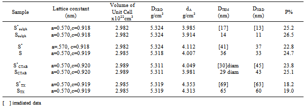
- XRD patterns of the investigated samples are presented in Fig. 1. For all samples (irradiated and unirradiated) the same patterns were observed with well developed( h k l ) reflections, which can be well indexed on the basis of the tetragonal spinel structure with the space group of I 41/a m d JCPDS file (71-2499)[7].
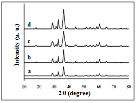 | Figure 1. XRD patterns of: a) S, b) SSulph, c) STX, d) SCTAB |
 Where the ions inside the square bracket are located in octahedral sites and the ions outside the bracket are in the tetrahedral sites.The crystallites size D, for the investigated samples were estimated from the Scherrer's equation[14] using the full-half line width of (311) peak:
 | (1) |
 | (2) |
 | (3) |
 From the table it is clear that the porosity decreases with increasing the particle size of the grains.
3.2. SEM and TEM
- Fig. 2a-b shows the scanning electron micrographs (SEM) and transmission electron images (TEM) of γ-irradiated and unirradiated samples. The morphology of the particles was found to depend on the type of surfactant used in the preparation method. TEM images of the sample prepared using CTAB surfactant showed dispersed nanorod particles. This may be attributed to either that CTAB can be worked as a capping agent or to the electrostatic interactions between the inorganic precursor and the CTAB surfactant to form inorganic- surfactant composite templates[20]. And because the spinel Fe0.1Zn0.9Mn2O4 is tetragonal in structure, therefore, the growth direction of the Fe0.1Zn0.9Mn2O4 nanorods can be determined as the[111] crystallographic direction. For the other samples prepared using sulphonic or triton surfactant the TEM-images showed nano particles with different shapes. Also, the morphology of the particles prepared in absence of surfactant showed particles do not have a well-defined morphology as shown in TEM micrographs. However, the images of the irradiated samples show to some extent a surface morphology slightly differs than that of unirradiated ones. Furthermore, the pores sizes became larger after the irradiation process. This indicates that the high ionization radiation may produce an effect on the surface of the sample. Inspection of Table 1 shows DXRD values differ to some extent than that of DTEM. This may be attributed to either the presence of non-crystalline materials at the lattice surface or to the different approach of two techniques. In XRD, the estimated crystal size showed the average size of the crystals, and the accuracy of the Scherrer equation is affected by many factors such as diffraction line width, defects, surface tension, so the Scherrer formula may induce some errors in measuring the absolute values of the crystallite size.
|
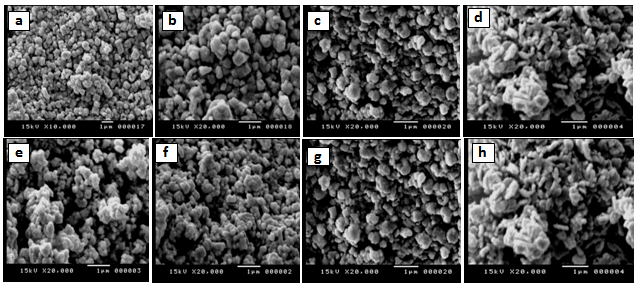 | Figure 2a. SEM for: a) S, b) SSulph, c) STX, d) SCTAB, e) S*, f) S*Sulph, g) S*TX, h) S*CTAB |
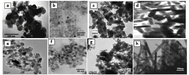 | Figure 2b. TEM for: a) S, b) SSulph, c) STX, d) SCTAB, e) S*, f) S*Sulph, g) S*TX, h) S*CTAB |
3.3. Electrical Properties
- The effect of particle size in nano range on electrical properties is important for mixed transition metals, not only from the application point of view but also from the fundamental point of view. Evaluation of dc– and ac-electrical conductivity reveals a wealth of information as regards the usefulness of these materials for various applications. Moreover, the study of dielectric constant sheds light on the behavior of charge carriers and the polarizability in the investigated material.
3.3.1. DC-Electrical Conductivity
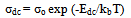
- The temperature dependence of dc-conductivity (σdc) for unirradiated samples is given in Fig. 3. The same behavior is also observed for irradiated samples. The electrical conduction can be explained according to:
 | (4) |
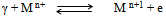
 Therefore, the hopping phenomena between Mn3+ and Mn4+ are responsible for the electrical conduction in the investigated system. The activation energy Edc has been calculated using least squares method and listed with other data in Table 2. From which it can be seen that the conductivity increases with increasing the particle size. This is due to the fact that the samples with small grains contain more number of grain boundaries than grains. Generally, the grain boundaries in nanocrystalline materials exhibit a random atomic arrangement without short or long range order[21]. The grain boundaries are the regions of mismatch between the energy states of adjacent grains and hence act as barriers to the flow of electrons. However, the obtained results refer to that the nature and volume fraction of the grain boundaries are very important in determining the electrical properties of consolidated nanoparticles.
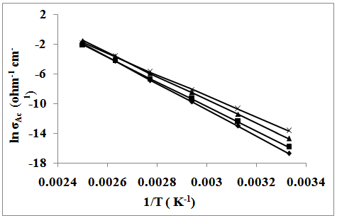 | Figure 3. The temperature dependence of DC conductivity of: (x), SCTAB; (▲), STX; (■), S; and (♦), SSulph |
|
 | (5) |
3.3.2. AC-conductivity
- In order to give information on the type of polarization present in the samples, the ac-electrical conductivity (σac), at temperatures range of 300-400 K and at frequency range of 102 – 106 Hz was studied. The ac-conductivity σac (ω) was calculated by subtracting the measured dc-conductivity (
 ) from the measured total frequency-dependent conductivity σt (ω) such that
 | (6) |
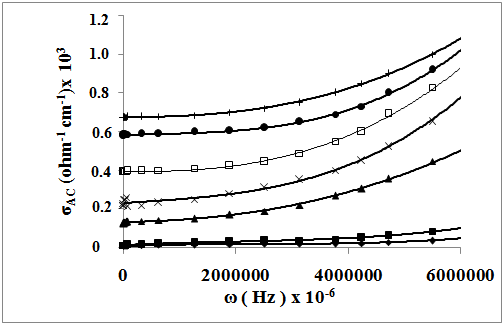 | Figure 4. The frequency dependence of AC-conductivity of : (♦), SSulph; (■), S; (▲), STX; (x), SCTAB(300K); (ӿ), SCTAB(340K); (●), SCTAB(380K); (+), SCTAB(400K) |
 | (7) |
3.3.3. Dielectric Behavior
- The frequency and temperature dependence of dielectric constant ε` and dielectric loss ε`` of nano Fe0.1Zn0.9Mn2O4 were studied. A similar trend is observed for all irradiated and unirradiated samples, some typical plots are shown in Fig (5, 6). It shows dielectric dispersion where both
 and
and  decrease rapidly with increasing frequency in low-frequency region while they approaches almost frequency independent behavior in high frequency region. The dielectric dispersion curve can be explained on the basis of Koop's theory[25] based on the Maxwell–Wagner model for the in-homogeneous double structure[26]. According to this model the dielectric structure was supposed to be composed of the double layer. The first layer is of fairly well conducting materials, which is separated by the second thin layer (grain boundaries) of relatively poor conducting substance. The grain boundaries were found to be more effective at lower frequencies while the manganite grains are more effective at higher ones. In present samples; Fe0.1Zn0.9Mn2O4 are dipolar materials due to the presence of different oxidation states in them. The electron exchange between these different oxidation states gives local displacement of electrons in the direction of applied electric field thus inducing polarization in manganite. The decrease in the dielectric constant with increasing the frequency is attributed to the decrease of polarization of the dipoles when electric field propagates with high frequency. The observed behavior can be also explained on the basis that in dielectric nanostructured materials interfaces are formed with a large volume fractions containing a large number of defects, such as dangling bonds, vacancies, vacancy clusters, and micro porosities. These can cause a change of positive and negative space charge distribution in interfaces. When these space charges are subjected to an electric field, they are moving and trapped by defects to form a lot of dipole moments. At low frequency region these dipole moments are easy to follow the change of the electric field[27]. Thus, the dielectric loss and hence the dielectric constant shows a large value at low frequency.For all investigated samples, ε` and ε`` increases with increasing the particle size. This can be explained on the basis of many factors, such as amorphousness of surface, high surface energy, micro mechanical stress, surface domain depolarization, domain wall effects, and so on. The obtained results showed also that each of ε` and ε`` increase with temperature. This is expected because as the temperature increases, the resistivity of the samples decreases and polarization increases. With the increase in temperature the thermal activation enhances the number of dipoles available for polarization.
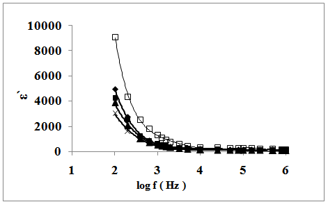 | Figure 5. The frequency dependence of dielectric constant of : (x), SSulph; (▲), S; (■), STX; ( ♦), SCTAB(300K); (ӿ), SCTAB(400K) |
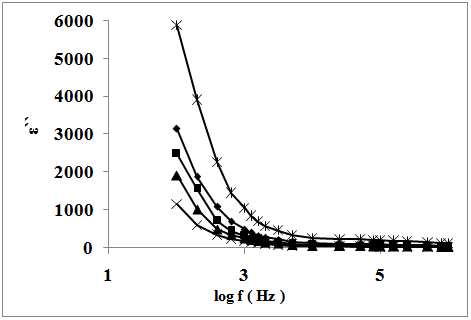 | Figure 6. The frequency dependence of dielectric loss of : (x), SSulph, (▲), S; (■), STX; ( ♦), SCTAB(300K); (ӿ), SCTAB(400K) |
3.4. Photocatalytic Activity
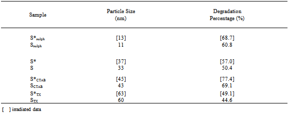
- In order to elucidate the effect of the size and morphology of Fe0.1Zn0.9Mn2O4 samples on the photocatalytic activity, a set of parallel experiments was conducted with prepared samples on methyl red (MR). Fig. 7 shows the degradation percentage, defined as (C0 − C) / C0 × 100 %, as a function of time, where C0 and C are the concentrations of MR before and after irradiation, respectively. It is well known that some dyes are degraded by direct UV radiation. Therefore, it should be examined to what extent the MR dye is ‘photolyzed’ if no catalyst was used. Blank experiments were carried out for the methyl red (MR) without catalyst for this purpose. The methyl red appears to be stable under irradiation without Fe0.1Zn0.9Mn2O4 photocatalyst, and the degradation percentage is less than 4% after 6 h UV irradiation. However, the introduction of Fe0.1Zn0.9Mn2O4 nanoparticles leads to a marked photo catalytic decomposition of the methyl red. After 6 h UV irradiation with samples S, Ssulph, SCTAB and STX, the MR degradation percentage reaches ~ 50%, ~ 61%, 77 and ~ 45%, respectively (see Fig. 7). The results are tabulated in Table 3. From which it can be seen that the photocatalytic activity increases with decreasing the particle size, except that for SCTAB sample with rod structure. This behavior was also reported by Hou et al.[28]. The photocatalytic activity of the γ- irradiated samples are found to be higher than that of unirradiated ones, Table 3. This may be attributed to the creation of lattice defects in the crystals and the change occurring in oxidation states of valence ions present in the samples due to gamma irradiation process.
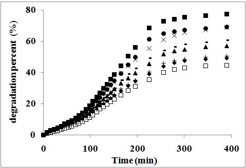 | Figure 7. The photocatalytic degradation of methyl red dye on irradiated and unirradiated samples: (■), S*CTAB; (●), SCTAB; (x), S*sulph; (-), Ssulph; (▲), S*; (+), S; (♦), STX*; (ӿ), STX |
|
4. Conclusions
- From the above results one can conclude the followings:-(1) X-ray showed a tetragonal spinel structure for all the investigated samples.(2) SEM analysis reveals that the morphology of the sample depends on the type of surfactant used. It shows also to some extent a surface morphology for irradiated samples differs than that of unirradiated ones. Moreover, the pores sizes became smaller after γ-irradiation process.(3) The conductivity value increases with increasing the particle size. The conductivity data showed semiconducting behavior and refer to a hopping conduction mechanism via electron transfer between valency states of transition metal ions present on octahedral sites for all irradiated and unirradiated samples.(4) Difference in conductivity data for the dc- and ac- conduction process is attributed to the effective drop of the electric field within the bulk due to the presence of space charge accumulations at the electrodes.(5) Interestingly, the as-prepared nanoparticles exhibit a pronounced photocatalytic activity for the decomposition of methyl red underultraviolet irradiation. The photocatalytic activity increases with decreasing the particle size and has the highest efficiency for the nano rod samples.