-
Paper Information
- Next Paper
- Previous Paper
- Paper Submission
-
Journal Information
- About This Journal
- Editorial Board
- Current Issue
- Archive
- Author Guidelines
- Contact Us
Science and Technology
p-ISSN: 2163-2669 e-ISSN: 2163-2677
2012; 2(5): 130-134
doi: 10.5923/j.scit.20120205.04
Structural Scheme of Information System for Defect Engineering of Dislocation-free Silicon Single Crystals
 Abstract
 Reference
 Full-Text PDF
 Full-Text HTML
V. I. Talanin , I. E. Talanin , N. Ph. Ustimenko
Department of Computer Science and Software Engineering, Institute of Economics and Information Technology, Zaporozhye, 69015, Ukraine
Correspondence to: I. E. Talanin , Department of Computer Science and Software Engineering, Institute of Economics and Information Technology, Zaporozhye, 69015, Ukraine.
| Email: |  |
Copyright © 2012 Scientific & Academic Publishing. All Rights Reserved.
The article is devoted to solving the problem of automation of the calculations and analysis of the defect structure of dislocation-free silicon single crystals. As a result, of development of information system kinetics of interaction of point defects at any time of crystal growth or heat treatments can be investigated. The solution to this problem will allow to simulate and to grow crystals with a predetermined defect structure, as well as manage it in the processes in subsequent technological treatments. The article presents the main aspects of information system for defect engineering of the dislocation-free silicon single crystals. The software structure and technology implementation has been considered. Structural scheme of information system was presented. It is assumed that with the help of this information system will be possible to control the defect structure at various stages of manufacture of devices based on silicon.
Keywords: Information System, Microdefects, Defect Engineering, Software
Article Outline
1. Introduction
- Modern electronic technology makes extremely high demands on the perfection of the crystal structure and homogeneity of distribution of electrical parameters in the bulk of grown single crystals and wafers made from them. The main role in the formation of grown-in microdefects in the grown single crystals played oxygen and carbon impurities and also intrinsic point defects (vacancies and interstitials)[1]. Manage the nature, content, size and pattern of distribution of microdefects depends on the development of effective methods of influence on the state of the ensemble of point defects in the ingot and wafers. Important role is played to study the influence of various thermal effects on the behavior of grown-in microdefects in wafers and on the strength characteristics of the wafers.In recent years has been made considerable progress in the theoretical description of the defect formation process during growth of dislocation-free silicon single crystals. Progress is based on the use of a diffusion model the formation of grown-in microdefects[2]. The basis of the diffusion model is the theoretically and experimentally established fact of the absence ofrecombination of intrinsic point defects at high temperatures[3]. Based on the elastic interaction between the intrinsic point defects and background impurities was first developed model of high-temperature precipitation of impurities during crystal growth. Model of high-temperature precipitation includes all three stages of classical theory of formation of second phase particles: critical nucleus formation, growth and coalescence of precipitate[4]. Precipitation process begins near the crystallization front and caused by the disappearance of excess intrinsic point defects at sinks. Sinks are oxygen and carbon impurities. We have shown that the critical nucleus size of precipitate near the crystallization front is minimal and increases with decreasing temperature during crystal cooling. It was confirmed that the formation of microvoids has the homogeneous character[5, 6]. The formation of interstitial dislocation loops is due to the deformation mechanism[7].In the general case in a growing single crystal determined four typical thermal zone[1]: (i) near Tc = 1683 K or in the vicinity of the crystallization front takes place the elastic interaction of point defects and absent recombination of intrinsic point defects; (ii) at T = 1682 ... 1423 K formed precipitates of impurities of oxygen and carbon; (iii) depending on the thermal conditions of growth at T = 1423 ... 1123 K, may be formed microvoids or interstitial dislocation loops; (iv) at T <1023 K takes place the growth of precipitates and formed the final pattern of distribution of grown-in microdefects in the single crystal. The influence of thermal conditions is investigated on the basis of mathematical models that describe the processes of formation of grown-in microdefects in the grown single crystals. In these models take into account the absence of recombination of own interstitial atoms and vacancies in the crystal near the crystallization front, and they allow you to predict the nature, size, density and distribution of grown-in microdefects in the bulk ingots[2].The most important in the modeling is the adequacy of the model that is, the degree of its compliance with the real processes. The main advantage of the diffusion model is dependence of characteristics of grown-in microdefects on the crystal growth parameters (growth rate, temperature gradients, cooling rate and the crystal diameter). This allowed us to create a new technique for the study of the dislocation-free silicon single crystals defect structure on the basis of modern information technology[8]. With this technique we have developed software for analysis of the defect structure of dislocation-free silicon single crystals grown by the Czochralski method and floating zone melting with diameters from 30 mm to 450 mm[8]. At the same time during technological effects on crystal the transformation of the initial defect structure is present. Therefore, the quality of silicon devices will be determined by the possibilities of human impact on all stages of their creation. The aim of our work is consideration establishing a information system for defect engineering in dislocation-free silicon single crystals based on an software which first declared in[8].
2. The Composition of Software Part of Information System
- In general case the solution of practical problems to improve the quality of silicon single crystals requires optimization of technological modes growth as a result of investigations of hydrodynamics of the melt and the complex conjugate heat and mass transfer in the plant of growth. The question of correlation of growth conditions and the volume of the crystallographic characteristics is extremely relevant. This question requires the prediction of hydrodynamics in the melt of boundary layer at the crystallization front, gas dynamics in the region above the surface of the melt and in the bulk the growth chamber, the temperature field in the crystal at all stages of growth. Solutions to this complex problem developed on the models of different levels and purposes: physical modeling, numerical modeling, an integrated approach. In recent years, are developing a global numerical models who pretend to calculate the complex conjugate heat and mass transfer throughout the growth chamber or in the thermal node[9,10]. They are a special case of three-dimensional hydrodynamic model for the system "crucible - melt - crystal"[11, 12]. At present, it becomes possible conjugate modeling with access to the management of the structural perfection of single crystal[13, 14]. In this case we assume conjugate solution of the three inter-related modeling tasks: (i) heat transfer processes in a modern thermal nodes of plant growth and the heat treatment of single crystal silicon; (ii) the stress state of single crystals and silicon wafers; (iii) the processes of defect formation in single crystals and wafers of silicon.Actual is construction of a unified model of defect formation, which provides prediction of features of microdefects formation at different stages of the process (crystal growth and follow heat treatment wafers).In[8] we proposed a new technique for studying the defect structure of silicon. This technique assumes modeling of the real experiments using software. Electronic equivalent of an object for direct test on the computer are programs that converted the mathematical models and algorithms to the available computer language (C++). The program is written high-level language programming in C++ compiler Borland C++ Builder. Program complex consists of two consecutive parts: (i) the unit determination the type of defect structure and (ii) the unit of calculation and graphs.However, this software has some significant drawbacks. These are: (i) one-dimensional modeling; (ii) used only for calculation of grown-in microdefects; (iii) the absence of modular construction of applications; (iv) the absence of class calculations and other. To address deficiencies and the accounting impact of technological treatments on the defect structure of silicon we propose to create a new model of information system using language C# on the platform .NET. We have developed a class of calculations the information system for the study of as-grown silicon single crystals. C# is fully object-oriented language, provides cross-platform, provides the tools and the ability to scale and development projects on the basis of this class, as well as the availability of suitable development environments for different operating systems.In contrast to the C++ object-oriented language C# has “garbage collection” function. This function enables avoid manual memory management and potential errors in the application. C# enables avoid mistakes when changing the code to provide flexible the compatible versions. The characteristic feature of C# is native support for interfaces and their inheritance. These features allow to develop complex systems and to develop their over time. C# allows the use of typed and extensible metadata, which can be attached to the object. Architecture of the project can be determined by local attributes that would be connected with any of the elements of language - classes, interfaces, etc. The developer may, with the help of the software to check the attributes of an element.Documenting code in C# is possible using XML documentations or XML documentation comments. They are contained in comments and describe the methods and properties in a particular file. Through this approach comments on the project are standardized. In addition, IntelliSense automatically displays information about the documented parameters and methods including built-in framework. At compile time generated XML file containing all data. To create the documentation for the code in Visual Studio C# in the comment field for special XML tags are included. Compiler that will compile with the parameter /doc, find the source code for all the XML tags to create an XML documentation file. To store the coordinates of the calculated graphs has been developed structure FloatPoint which is in contrast to the base structure of the Point stores the values of type double, not int. The class encapsulates all the values of the variables needed to calculate. To work with the values used by setter and getter functions, since directly with the variables can not work for reasons of security and the concept of object-oriented programming. To initialize the class are used two constructors: standard constructor and constructor with parameters. The last constructor specifies the parameters required for the first calculation and determination region of further calculations. In the class there are properties and methods for obtaining the names of the methods (Czochralski or floating zone melting), the parameters of defects (loops, precipitates, microvoids), allowable sizes for each method and the numeric equivalents of these values is necessary for the correct operation of the class. Developers can use these methods to populate the user interface elements associated with the choice of these parameters. In class there is method to calculate the first graph and determine areas for further calculations. Also, there is three methods for the calculation of 1, 2 and 3 regions, respectively[8]. They return an array of pixels FloatPoint with values required for plotting graphs. The class also uses private methods required for internal calculations. Their number will increase during the code optimization.With the use of this class has developed several software products. For example, (i) the information system for the study of as-grown silicon single crystals which is a desktop application for Linux, Windows and MacOS, (ii) Web-service with an API and web-shell in the form of the site working with the API. In the second product we will be able to shift all the calculations on the server (or servers) what affect the increase in performance and speed calculations. Clients will only to introduce parameters and receive the results of calculations. This system can be used on older computers for which the calculations are too time-consuming, and on mobile devices with a modern browser.
3. Structural Scheme an Information System
- In Fig. 1 shows a scheme of an information system. The information system contains two blocs: (i) bloc the calculation of grown-in microdefects and (ii) the bloc calculation postgrowth microdefects. On the input module received the values of the parameters of growth of dislocation-free silicon single crystals (method of growing, growth rate Vg, axial temperature gradient G, Voronkov’s parameter C = Vg/G[15], crystal diameter). The output module gives information about the type of defect and its size and concentration.The first area of the calculation is characterized by high rates of crystal growth, when formed only microvoids and precipitates. The second area of calculation is characterized by the average growth rate of the crystal, when a ring of precipitate in the plane perpendicular to the direction of growth crystal is formed. In this case inside the ring are formed precipitates and microvoids, outside the ring are formed precipitates and interstitial dislocation loops. The third area of calculation is characterized by low rates of crystal growth, when the are formed precipitates and interstitial dislocation loops. Mathematical models and calculation parameters are given in[2, 4, 16].To calculate the formation of grown-in microdefects been used two mathematical approaches: the analytical calculations (I) and approximate calculations (II). In the case of (I) it is a solution of differential equations of the dissociative diffusion.In the case of (II) solution is sought in the form of systems of interconnected discrete differential equations of the quasi-chemical reactions to describe the initial stages of nucleation of new phases, and a similar system of continual differential equations of the Fokker-Planck equation[2].
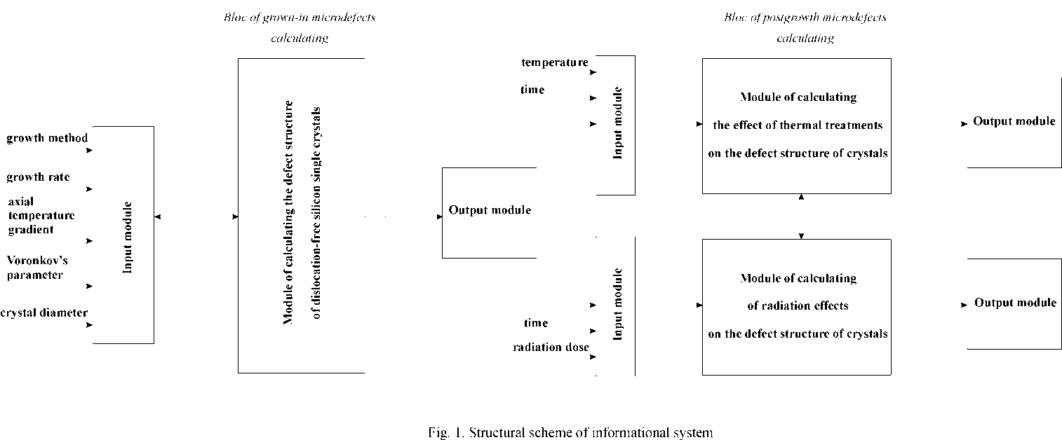 | Figure 1. Structural scheme of informational system |
4. Conclusions
- The task of construction the defect structure of dislocation-free silicon single crystal is an inverse problem the analysis and calculation of grown-in microdefects. In this case, you must first specify the type, size and concentration of grown-in microdefects. Parameters of grown-in microdefects are selected based on the requirements for defect structure of devices and integrated circuits. In the next stage are calculated parameters of crystal growth (the growth rate for a certain diameter of the crystal and temperature gradients), which provide presence of given defects of structure. We get that the defect structure determines thermal conditions of crystal growth. To automate the process of crystal growth need to carry out the development of software products based on the diffusion model in combination with known software products for modelling crystal growth[1].Production technologies of devices based on silicon technology are connected with various impacts on the material. Heat treatments, ionizing radiations and mechanical effects have a critical impact on the initial defect structure of dislocation-free silicon single crystals. Technological impacts are lead to the transformation of grown-in microdefects. In the general case technological impacts are leads to: (i) the growth of initial grown-in microdefects; (ii) formation on grown-in microdefects of new defects (e.g., stacking faults); (iii) the formation of new defects. In contrast to grown-in microdefects these defects of crystal structure can be defined as postgrowth microdefects[1].Proposed system is a specialized information system which is software of dual-use. On the one hand it is a virtual experimental device for investigation of the processes of defect formation in growing single crystals and devices based on silicon. On the other hand using the software can determine the conditions for crystal growth and its mode of treatment for a well-defined defect structure. In the basis of the information system laid modern models and methods of modeling. Software products are based on a thorough understanding of physical processes and the use of modern numerical methods for solving nonlinear multidimensional conjugate problems and offer user-friendly interface. Software allows users with minimal computing experience to effectively apply them in solving engineering and research tasks.The information system allows for minimizing the financial cost to develop the scientific basis of modern technologies for producing single crystals and large-scale wafers with the necessary characteristics. The information system can be used in future to optimize the constructions of thermal furnace of the semiconductor industry and temperature-dynamical conditions of crystal growth and the time-temperature heat treatment of plates that guarantee control of the nature, content, size and distribution of these microdefects. Creation an information system was made possible after building a unified (full) model of defect formation which provides prediction of features of formation of microdefects at different stages of the technological process (growth of single crystal and the subsequent technological treatment wafers).