G. K. Solanki 1, Dipika B. Patel 1, K. D. Patel 1, N. N. Gosai 2, Yunus Gafur Mansur 3
1Department of Physics, Sardar Patel University, Vallabh Vidyanagar, Gujarat, India.
2Faculty of Engineering, Marwadi Education Foundation’s Group of Institutions, Rajkot
3The Patidar GIN Science College, Bardoli, Gujarat
Correspondence to: G. K. Solanki , Department of Physics, Sardar Patel University, Vallabh Vidyanagar, Gujarat, India..
| Email: |  |
Copyright © 2012 Scientific & Academic Publishing. All Rights Reserved.
Abstract
The present paper reports the growth of GeS0.25Se0.75 single crystals by direct vapor transport technique (DVT) using two zone horizontal furnace. The precise adjustment of the temperature gradient between source and growth zone of a horizontal furnace that enhance the transport of material in vapor form could result in the growth of gray, shining thin flakes of GeS0.25Se0.75 single crystals. The average dimensions of grown crystals were 0.90 x 0.56 cm2. As grown GeS0.25Se0.75 single crystals were used for dielectric measurement. The dielectric measurements were carried out by standard two electrode method using HP4284A LCR meter and a digital temperature controller DT4284. The entire measurement cycle was programmed by LABVIEW software. The dielectric properties i.e. capacitance (C) alternating current conductivity (σac) and dielectric constant (ε’) are measured in the frequency range 100 Hz to 1 MHz with different temperature from room temperature to 523 K, in the step of 50 K temperature using 4284A LCR meter. In this investigation, dielectric constant is observed to be high at lower frequency and it systematically decreases with increasing frequency up to 600 kHz and then after it nearly becomes frequency independent while dielectric loss tanδ decreases with temperature and frequency.
Keywords:
GeS0.25Se0.75 Single Crystals, Vapor Transport Technique, Dielectric Constant, a. c. conductivity
Cite this paper:
G. K. Solanki , Dipika B. Patel , K. D. Patel , N. N. Gosai , Yunus Gafur Mansur , "Growth and Dielectric Properties of DVT Grown GeS0.25Se0.75 Single Crystals", Physical Chemistry, Vol. 2 No. 5, 2012, pp. 67-72. doi: 10.5923/j.pc.20120205.02.
1. Introduction
The study of dielectric behaviour of chalcogenides materials is expected to reveal structural information which, in effect, can be useful for the understanding of conduction mechanism as well. In addition, a study of temperature dependence of dielectric permittivity particularly in the range of frequencies where dielectric dispersion occurs can be of great importance for the understanding of the nature and origin of the losses occurring in these materials[1]. Now a days, the negative capacitance effect has been displayed in a variety of electronic devices, such as p- n junctions[2], metal- semiconductor Schottky diodes[3, 4], GaAs/ AlGaAs quantum well infrared photodetectors (QWIPs) and GaAs homojunction far infra red detectors. The microscopic physical mechanisms of the negative capacitance in different devices are obviously different and have been ascribed mainly to the contact injection, interface states, or minority- carrier injection[5]. Negative capacitance has been observed by various workers in amorphous chalcogenide films, in structures of the type metal- insulator- metal, semi- insulating polycrystalline silicone, etc.Recently, the physical properties of such type of layered materials have been a field of intensive study. And due to their electrical and optical properties, the binary IV-VI layered semiconducting compounds produced a great deal of interest and applications in different fields[6]. An interesting group of compounds which has received increasing attention from the fundamental as well as the industrial or application point of view. The study of dielectric properties of solids often gives good insight into the electric field distribution within the solids. Studying the dielectric constant as a function of frequency and temperature, the various polarization mechanisms in solids can be understood. It attracts attention in infrared optoelectronic devices, radiation detectors, holographic recording system, electrical switching, polarity dependent memory switching and solar cell fabrication[7].
2. Experimental
2.1. Growth
In the present investigations GeS0.25Se0.75 crystals have been grown by direct vapor transport (DVT) technique. Two zone horizontal furnace having required dimensions has been used which is shown in Figure 1. The furnace was constructed by a special sillimanite threaded tube closed at one end, 450 mm in length, 70 mm outer diameter, 56 mm inner diameter with threaded pitch of 3 mm, imported form from koppers Fabriken Feuerfester, Germany. High quality quartz ampoules were used for growth experiment having dimensions of 24 cm length, 2.4 cm outer diameter and 2.2 cm inner diameter. 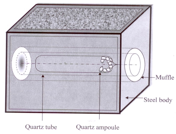 | Figure 1. The dual zone horizontal furnace with co-axially loaded ampoule |
For compound preparation the cleaned ampoule was filled with stoichiometric proportion of Ge (99.999%), S (99.99%) and Se (99.99 %) pure of about 10 g for growth then ampoule was sealed under pressure of 10-5 Torr. The sealed ampoule was kept in two-zone horizontal furnace. The temperatures of both the zones were slowly but gradually raised up to desired temperature and maintained that temperature for specific time, after that furnace was cooled off at the room temperature. Detailed growth parameters are mentioned in Table 1. The ampoule was broken and shaken well with help of agate mortar to prepare fine powder of this compound.| Table 1. Growth condition for GeS0.25Se0.75 single crystals |
| | Crystal | Temperature | Growth Period (hours) | Dimensions of grown Crystal (cm2) | | GeS0.25Se0.75 | Reaction Zone (K) | Growth Zone (K) | 168 | 0.90 X 0.56 | | 1073 | 1023 |
|
|
2.2. High Temperature LCR Measurement Set Up
The grown crystals or pallets of GeS0.25Se0.75 may be used directly for dielectric study. The geometrical dimension of used sample was measured by a travelling microscope and the thickness has been measured by micrometer screw. The dielectric measurements were carried out using two standard electrode method. The specimen was mounted in between two flat stainless steel parallel electrodes of a specially designed sample holder. Both the upper and lower base of the holder can be screwed in four proper contact of the sample with the electrode. The sample holder was enclosed in a specially built resistance heating furnace which is capable to provide temperature up to 623 K. We have measured dielectric parameters automation and controlling software ‘LABVIEW’ is used. The parameters like the thickness and area of the sample, starting and ending temperature and frequency have been set in software. These input data are essential in order to measure the dielectric properties at desired temperature and frequencies. The digital temperature controller DT84848 is used to monitor the preferred temperature of the specimen. When preferred temperature is achieved HP4284A LCR meter will scan all the frequencies and resultant data is stored in the storage device.
3. Results and Discussion
3.1. Basics of Dielectric Studies
The capacitance, dielectric constant and dielectric loss are important parameters in the selection of materials for device application. The dielectric constant ε’ is evaluated from the equation, | (1) |
where C is the capacitance of the pellet (F), d is the thickness of the pellet (m), ε0 is the permittivity of free space (ε0 = 8.85 × 10⁻¹² F m−1) and A is the area of the electrode (m2). The imaginary part of the dielectric loss (ε’’) of the various frequencies was calculated using the measured conductance values (G) from the relation, | (2) |
where G is the dc conductance of the sample, and ω (= 2πf) is the angular frequency. The dielectric loss tan δ was calculated from the relation[8], | (3) |
The alternating current (ac) conductivity σac is calculated using the relation, | (4) |
where f is the frequency of the applied ac field (Hz).
3.2. Variation in Dielectric Parameters with Frequency
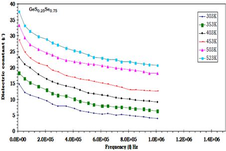
As one can see from figure 2, that dielectric behavior is frequency dependant as well as temperature dependent. The capacitance is decreases with temperature and it decreases with increasing frequency for GeS0.25Se0.75 compound. Because at lower temperature the mobility of ions is very low and so is the conductivity, resulting a lower value of capacitance. With temperature, the mobility of charge carriers increases, resulting the increase in space charge polarization and capacitance both.From Figure 3, the dielectric constant is observed to be high at lower frequency and it systematically decrease with increasing frequency. The dielectric constant of solids is known to consist of contribution from electronic, ionic, dipolar and space charge polarization exhibits itself prominently at lower frequency. Frequency dependence value of ε’ is taken as static dielectric constant. 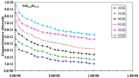 | Figure 2. Variation of capacitance and dielectric constant with frequency at different temperature |
 | Figure 3. Variation of capacitance and dielectric constant with frequency at different temperature |
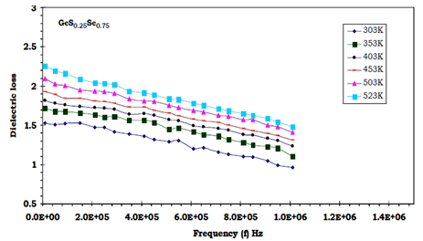 | Figure 4. Variation of dielectric loss and imaginary part of dielectric constant with frequency at different temperature |
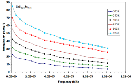 | Figure 5. Variation of dielectric loss and imaginary part of dielectric constant with frequency at different temperature |
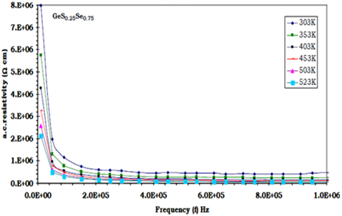 | Figure 6. Variation of a. c. resistivity and a. c. conductivity with frequency at different temperature |
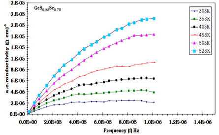 | Figure 7. Variation of a. c. resistivity and a. c. conductivity with frequency at different temperature |
The temperature is also found to exhibit an interesting influence on the dielectric properties. The value of ε’ decreases with temperature for the grown compound/ sample. From earlier discussion one can notice that at low temperatures the variation in dielectric constant is much less frequency dependant, while at higher temperatures the increment in dielectric constant is stronger and much more frequency dependant. This is due to lattice expansion, polarizability of the constituent ions due to increase of atomic polarizability[9]. The changes in ε’ with temperature are of similar nature at all the frequencies. The variation in dielectric loss tan δ (i. e. Figure 4), it decreases with increasing frequency and it increases consistently with temperature for GeS0.25Se0.75 crystals. For many materials it has been observed that the dielectric loss decreases as frequency increases[10, 11]. The response of the normal materials to applied fields depends on the frequency of the applied fields. In fact, polarization of material does not respond instantaneously to an applied field so the permittivity is often treated as a complex function of frequency. The change in complex/ imaginary dielectric constant with frequency is shown in Figure 5, indicates that as the frequency increases the value of imaginary part of the permittivity decreases. And also it decreases with temperature for GeS0.25Se0.75 crystals. The observed decrease in ε’’ values with frequency and decrease in ε’’ with temperature, which are the common features of all the compositions and it can be on explained on similar arguments as for dielectric constant ε’[12, 13].Such type nature of dielectric properties was found in the semiconductor films which were obtained by deposition of germanium monosulphide at an evaporation temperature of 725 K in vacuum[14]. The frequency dependence of the capacitance and dielectric loss of the systems could be described satisfactory over a wide interval up to 107 Hz. In the frequency range 105- 107 Hz, C and tanδ exhibit constant values. At high frequencies above 107 Hz, a decrease in C was observed together with a sharp increase in tan δ. The temperature dependence of the capacitance and dielectric loss were studied in the range 150- 400 K. The dependence of these parameters on frequency was investigated in the range 400- 4x10⁷ Hz. This temperature range and frequency range is almost same as our set up range but difference is that we had performed experiment on GeS0.25Se0.75 compound instead of GeS films. Dependence on frequency of the dielectric loss at different temperatures with the relative permittivity ε normalized to its values at 293 K and 1 kHz. In the temperature range studied 153- 393 K, the relative permittivity variation is insignificant but it shows a slight tendency to increase as the temperature increases. The dielectric permittivity ε retains the value of 10 in the frequency interval from 400 to 10000 Hz. The dielectric loss hardly alters with frequency and temperature changes. The greatest increase in tan δ is observed between 323 and 383 K especially at lower frequencies where the loss exhibits an increase up to 500 % with respect to that at 323 K. The conductivity of all the materials is increases with temperature and frequency both while at higher frequency it is much more independent of frequency with compared to that lower frequency range. The resistivity decreases with frequency and temperature both with can be seen from Figure 6. So at higher temperature GeS0.25Se0.75 single crystals become more conducting so its resistivity decreases with temperature. Figure 7 shows that at lower frequency the increase in conductivity is more rapid and at higher frequency the conductivity increases very slowly.
4. Conclusions
Here we have grown successfully GeS0.25Se0.75 single crystals using vapor transporting technique and dimension of as grown crystals are enough to use in device application as well as for characterization purpose. From dielectric study, we shown and explain with physical significance that how all the dielectric properties i.e. capacitance (C), alternating current conductivity (σac), dielectric constant (ε’), dielectric loss tanδ and imaginary dielectric constant (ε’’) are being changed as a function of frequency and temperature. Hence, temperature dependence of dielectric properties in the said range of frequencies where dielectric dispersion occurs being of great importance for the understanding of the nature, origin of the losses occurring in these materials and use of these material up to 523K temperature in the device fabrication.
ACKNOWLEDGEMENTS
Authors are thankful to UGC, New Delhi, India for the sanctioned of a major research project to G. K. Solanki which provided the necessary financial help for carrying out this work.
References
| [1] | Sharma J., Kumar.S., Journal of Ovonic Research Vol,6(1), (2010) 35- 44. |
| [2] | Okawa, Y.; Norimatsu, H.; Suto, H.; Takayanagi, M., International conference on Microelectronic Test Structures, IEEE Xplore, March (2003). |
| [3] | Wu X, Yang E S and Evans H L, J. Appl. Phys 68, (1990) 2845. |
| [4] | Champness C H and Clark W R Appl. Phys. Lett. 56, (1990) 1104. |
| [5] | S Cavdar, H Koralay et al. Supercond. Sci. Technol 18 1204- 1209. |
| [6] | G. K. Solanki, K. D. Patel, N. N. Gosai and K. Hingarajiya. International Journal of Manufacturing Science and Engineering, Vol 2, No. 2 (2011) 85-87. |
| [7] | G. K. Solanki, K. D. Patel, Rahul B. Patel, Sandip Unadkat, Dipika B. Patel and N. N. Gosai, Journal of Optoelectronics and Biomedical Materials 2, (3), (2010) 99-107. |
| [8] | C. P. Smyth, “Dielectric Behaviour and Structure”, John- Willey & Sons, New York, 132 (1953) |
| [9] | Suresh S, Research Journal of Chemical Sciences, Vol. 2(2), (2012) 83-86. |
| [10] | B. B. Parekh and M. J. Joshi, Cryst. Res and Technol. 42 (2007) 127. |
| [11] | B. B. Parekh, P. M. Vyas, Sonal R. Vasant and M. J. Joshi, Bull. Mater. Sci. 31(2008) 143- 147. |
| [12] | B. B. Parekh and M. J. Joshi, Cryst. Res and Technol. 42, (2007) 127 – 129. |
| [13] | S. S. Sastry, G. Satyanandam, A. Subrahmanyan and V. R. K. Murthy, Phys. Stat. Solidi, K71 (1988) 105. |
| [14] | A Stanchev and C. Vodenicharov, Thin Solid Films, 29 (1975) L13- L16. |
 Abstract
 Reference
 Full-Text PDF
 Full-Text HTML