-
Paper Information
- Paper Submission
-
Journal Information
- About This Journal
- Editorial Board
- Current Issue
- Archive
- Author Guidelines
- Contact Us
International Journal of Optics and Applications
p-ISSN: 2168-5053 e-ISSN: 2168-5061
2019; 8(1): 12-20
doi:10.5923/j.optics.20190801.03

Demonstration of Compact Free-Space Optical MIMO Transmitter and Receiver Using Tri-Wavelength VCSELs and Silicon APDs
 Abstract
 Reference
 Full-Text PDF
 Full-text HTML
Christopher White, Clifton R. Haider, Daniel J. Schwab, Barry K. Gilbert
Special Purpose Processor Development Group, Mayo Clinic, Rochester, MN, USA
Correspondence to: Christopher White, Special Purpose Processor Development Group, Mayo Clinic, Rochester, MN, USA.
| Email: |  |
Copyright © 2019 The Author(s). Published by Scientific & Academic Publishing.
This work is licensed under the Creative Commons Attribution International License (CC BY).
http://creativecommons.org/licenses/by/4.0/

The use of multi-wavelength optical tests can be found in many applications including industrial manufacturing, food testing, and hospitals. This effort was targeted at making compact devices that could emit multiple wavelengths and detect multiple wavelengths simultaneously. Multiple approaches were considered. The chosen design accomplishes multiple input and multiple output spectral measurements through a direct-sequence spread spectrum (DSSS) technique. The devices demonstrated within this paper are novel in that they allow simultaneous operation of multiple wavelengths and multiple detectors using readily available components in a compact arrangement.
Keywords: Free-space optics, Spectrometer, MIMO, APD, VCSEL
Cite this paper: Christopher White, Clifton R. Haider, Daniel J. Schwab, Barry K. Gilbert, Demonstration of Compact Free-Space Optical MIMO Transmitter and Receiver Using Tri-Wavelength VCSELs and Silicon APDs, International Journal of Optics and Applications, Vol. 8 No. 1, 2019, pp. 12-20. doi: 10.5923/j.optics.20190801.03.
Article Outline
1. Introduction
- The measurement of the optical parameters, such as scattering and absorption, can be used to discern key information about media within a test environment. Further, the use of multiple wavelengths for optical testing of media can be collectively analysed as a measure of specific materials, chemicals, structures, etc. within a medium [1] [2]. The use of multi-wavelength optical tests can be found in many applications including industrial manufacturing, food testing, and hospitals.This effort was targeted at making compact devices that could emit multiple wavelengths and detect multiple wavelengths simultaneously. Multiple approaches were considered. Time multiplexing the wavelength sources would allow a single sensor to measure each of the wavelengths without interference from other test wavelengths [1]. Separate detectors could be selected for each wavelength, thereby allowing for simultaneous measurements. However, these approaches have drawbacks. Time multiplexing limits the ability to make measurements of time varying media. Separate detectors would require more components, which would grow the size of the devices [2].The devices described below are novel in that they avoid time multiplexing using readily available components in a compact arrangement. A compact device allows testing in confined spaces, testing around small samples, or even on human volunteers. The benefit of simultaneous measurements is that time varying media can be measured quickly across multiple parameters. When the measurement requires the same condition for each wavelength, such as in pulse oximetry [3], simultaneous optical measurements of the media will increase the accuracy of the test.This design accomplishes simultaneous wavelength measurements through a direct-sequence spread spectrum (DSSS) technique [4]. The DSSS implementation uses a unique maximal length code sequence for each wavelength in the system. The receiver’s photodetector detects all of the wavelengths simultaneously and creates an electrical output that is the superposition of all signals from all wavelengths. The post-processing of the electrical signal benefits from DSSS in two ways. First, the code sequences are uncorrelated so that correlating the electrical signal with one of the codes will effectively filter out all other wavelengths. Second, the optical losses are anticipated to be substantial. The DSSS technique inherently boosts the signal-to-noise ratio (SNR) at the output of the system.Optical measurements sometimes need to be measured at different locations along a medium to assess optical parameters of the medium [5]. For example, measurements at multiple locations separated from a source can be used to identify the absorption of each wavelength within an unknown medium. Therefore, this design incorporates two isolated receiver front ends that are separated by a fixed distance in a coplanar arrangement along the receiver PCB.In this paper, we present the design and test of a multiple-input multiple-output transmitter and receiver using commodity components. The use of commodity fiber optic communications components such as Vertical Cavity Source Emitting Lasers (VCSELs) and semiconductor photodetectors may permit higher performance with improved component availability as well as an improved price-to-performance ratio. Section II discusses the design methodology, component selection, and assembly of the transmitter and receiver. Section III describes the testing and results, highlighting the system’s performance.
2. Design
- The transmitter front end comprises three laser drivers and three VCSELs. The VCSELs are at three different wavelengths: 680 nm, 790 nm, and 850 nm. The receiver front end contains two photodetectors, two transimpedance amplifiers (TIAs), and several gain stages. The complete transmitter sends a repeated unique maximal length code sequence for each wavelength. The complete optical receiver detects the optical waveforms and separates the wavelengths by correlating the received waveforms with each wavelength’s unique maximal length code. The choice was made to implement each sequence generation with a pattern generator driving non-return to zero (NRZ) symbols based on a predetermined repeating maximal length code [6]. The receiver signal recovery was implemented in software to allow us to concentrate on the design and testing of the optical front ends.
2.1. Optical Front End Design Process
- During the first phase of the design process, we created an optical power budget analysis. Figure 1 depicts the measurement setup. The three primary components are the transmitter, the transport medium, and the receiver. The transmitter includes the signal source, the laser drivers, and the directly modulated lasers. The receiver incorporates the photodetectors, the TIA, gain stages, and analog-to-digital converters (ADC) that sample the received signals.
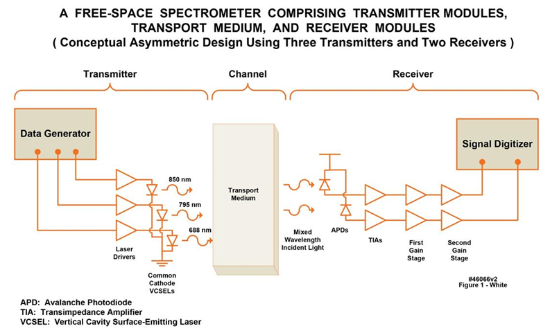 | Figure 1. The free-space, three wavelength spectrometer described herein comprises three transmitter modules, a common transport medium, and two receiver modules. (46066) |
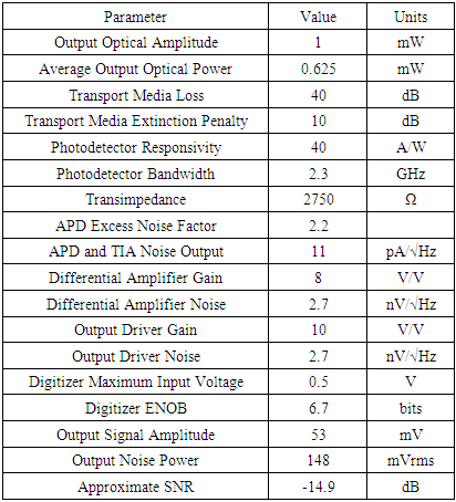
2.1.1. Link Loss Budget
- To design the transmitter and receiver modules, an estimate of the link budget was calculated, which provided a definition of component requirements. The link budget for the design appears in Table 1, which assumed an optical attenuation of 40 dB and an extinction penalty of 10 dB. The calculation of the SNR assumes that the output signal is a square wave and that the noise is Gaussian, yielding an estimated SNR of -14.9 dB. The parameters related to a notional receiver design are depicted in Figure 2.
 | Figure 2. The receiver has four primary components: the photodetector, the bias control circuitry, the transimpedance amplifier, and the output amplifier. (44754) |
2.1.2. Optical Modulator Design (Figure 3, Right Panel)
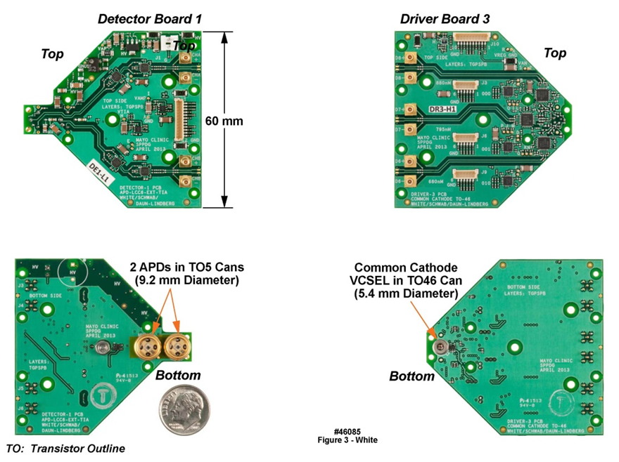
- The transmitter module required three independent lasers, with a unique data sequence transmitted by each laser. VCSELs from Vixar, Inc. were selected, specifically the MULTM-0000-B001 component, which comprises three VCSELs in one TO-46 can. Each VCSEL has an isolated anode pin, but all three share a common cathode pin. The three lasers have wavelengths of 670 nm, 795 nm, and 850 nm. The Texas Instruments’ ONET4211LD laser driver was selected to bias, monitor, and modulate the VCSEL. Three separate components were used, one for each laser. This configuration allowed independent control of each VCSEL. The use of a common cathode triad of lasers did not connect in an optimal manner to the laser drivers, because traditional fiber optic lasers use a common anode package. To overcome this issue, we created an alternate circuit design for the laser drivers. The anode of each laser was connected with an 18 Ω resistor to the positive supply voltage. The laser driver was connected to the anode as well. Thus, the VCSELs were modulated by means of voltage compression.
 | Figure 3. The transmitter module has one TO-46 can comprising three VCSELs. Each VCSEL is driven with an ONET4211LD laser driver. (44143) |
2.1.3. Optical Receiver Design (Figure 3, Left Panel)
- The detector converts the light into electrical current. The detector’s material determines the spectrum of light that the detector can most efficiently convert. For the sub–1000 nm wavelengths, a silicon detector demonstrates the best performance. Two common forms of detectors are PIN photodiodes and avalanche photodiodes (APDs) [7] [10]. A PIN photodiode converts light to electrical current with a responsivity of approximately 0.6 amps/watt (A/W). An APD converts light to electrical current as well, but it has an additional gain factor which can increase the responsivity by 10-100 times that of a PIN photodiode. However, concomitant with the higher gain, the APD also contributes additional noise to the signal.Typical optical communication receiver circuits contain bias circuitry to cancel the dark current and static light current from the photodiode, as illustrated in Figure 2 [11] [12]. Because the bias circuitry is a feedback control loop, the receiver typically has a low frequency bandwidth cutoff in the kilohertz range. This circuitry is critical for this specific application, because it can subtract the ambient light current from the signal as long as the ambient light level is nearly constant within the response time of the circuitry.Once the light signal has been converted to electrical current, the signal needs to be amplified. A transimpedance amplifier (TIA) is traditionally used to amplify and simultaneously convert the current signal to a voltage waveform, but also adds electrical noise to the received signal. The totality of the noise is determined by many factors including the TIA’s bandwidth and its transimpedance value [10]. The transimpedance stage is designed to accommodate the photodiode capacitance, to deliver a specifically defined bandwidth, as well as an optimal signal to noise ratio.We selected the AD230-2.3G-TO5 APD with integrated TIA from Pacific Silicon Sensor, packaged in a TO-5 can. The APD has an active area of 0.042 mm2 and a peak responsivity of 50 A/W near 800 nm, a gain of 100 at approximately 150 V, and an excess noise factor of 2.2. The TIA has a transimpedance of 2.75 kΩ and a bandwidth of 2.3 GHz. The output of the TIA is linear with respect to the input current up to 40 µA peak-to-peak (p-p), at which point the output voltage begins to saturate.The output of the TIA is typically too small at low light levels for a typical communications receiver to detect. Therefore, one or multiple gain stages may be needed following the TIA, which can boost the signal to the necessary amplitudes for detection [13]. However, the gain stages also amplify any prior noise contaminants and contribute additional noise as well. Thus, the gain and noise of these stages must be tailored to allow the best possible signal to noise ratio.The bandwidth and linearity of the output amplifiers are critical to overall system performance [13]. For traditional optical communications receivers, the output amplifiers are actually limiting amplifiers [11] that drive the signal to a fixed low or high voltage; such stages have wide bandwidth but are strongly nonlinear. Code-division multiple access (CDMA) receivers, which are also spread spectrum, employ integrate-and-dump circuits [10] [14] that are also nonlinear. For this application, a limiting amplifier would distort the signal and prevent successful correlation with the known code sequence. Alternately, the integrate-and-dump circuitry can be replaced with digital post-processing. Therefore, the output stages were required to have minimal distortion across the supported signal band [15].For this design, we selected the AD8352 from Analog Devices. Two AD8352 amplifiers were used consecutively to provide the desired signal gain while delivering adjustable bandwidth up to 2 GHz. The first instance of the amplifier was configured to provide roughly 20 dB of gain, while the second instance was configured to drive the signal into a NI-5186 digitizer from National Instruments.
3. Results
3.1. Component Characterization
- The transmitter module was initialized by setting the appropriate drive currents to achieve maximum output amplitude for each VCSEL, using digital potentiometers to set the bias and modulation currents. The three panels in Figure 4 display the waveforms for each VCSEL output using a 27 – 1 pseudo-random bit sequence (PRBS) pattern at 1.25 Gbit/s. The pattern generator’s singled-ended outputs were connected to SHF Communication Technologies AG baluns to create differential signals as the input to each laser driver. The outputs of the VCSELs were measured using a fiber probe connected to a Tektronix DSA8200 digital oscilloscope with the 80C08C 10 Gbit/s optics module. Because the fiber probe could not capture all of the light from the VCSELs, the measured amplitudes were much smaller than the total emitted light power. In addition, the large overshoot on the rising edges of the pattern is a known characteristic of VCSELs. As anticipated, the optical signal exhibited sharp edges, delivering a nearly ideal square shape.
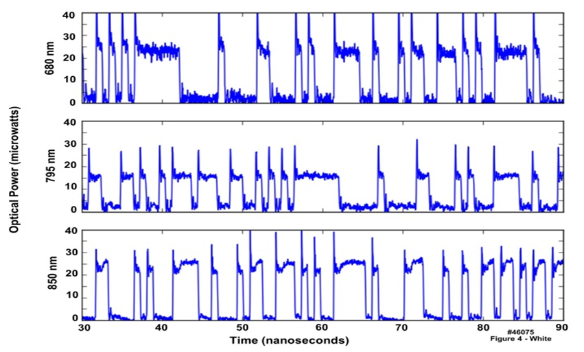 | Figure 4. Output of the three VCSELs as captured on a Tektronix DSA8200 with an optical module. These waveforms illustrate a PRBS sequence of 27-1 pattern. (46075) |
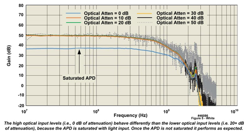 | Figure 5. Receiver gain for a single-ended output as measured by an Agilent optical spectrum analyzer (OSA). The optical attenuation was swept from 0 dB to 60 dB. The isolated lower gain curve occurs when the APD is saturated with light. (46086) |
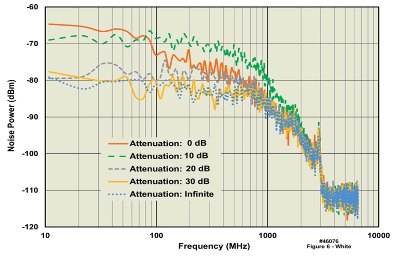 | Figure 6. Receiver noise power was measured on a spectrum analyzer. The input optical power was from an 850 nm light source without modulation. The light was attenuated to illustrate the noise power for decreasing levels of incident light power. (46076) |
3.2. Intermediary Measurement Demonstration
- To complete the analysis of the transmitter and receiver pair, a test setup was constructed that allowed the insertion of various media between the light source and the detectors. The test media consisted of a cuvette filled with an intralipid diluted to various concentrations. The setup allowed for the devices to be arranged in different positions to discern the difference in absorption dominant and scattering dominant scenarios. The overall object of the testing was to demonstrate the capability of the DSSS post-processing.The components were combined to test a target sample of intralipid-20%. The test solution was diluted with de-ionized water. A ratio of 1 part intralipid was combined with increasing parts of water. The variations of water proportions were 2, 4, 8, 16, and 32. The greatest proportion of water created a sample with a concentration less than 1% intralipid.In Figure 7, the system was oriented to test the sample in three different configurations. Each configuration represents traditional optical measurement techniques. Also, each configuration exposes a different relationship between the scatter and absorption behaviors of the test sample. A “through” configuration favors the measurement of absorption. The orthogonal measurement offers a balance of absorption and scattering depending on the divergence of the VCSEL beams. The same-side configuration favors scattering and reflectance measurements.
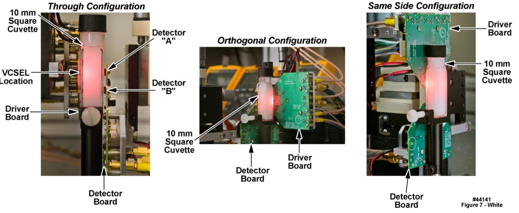 | Figure 7. Test configurations of the multi-wavelength and multiple detector optical front ends. (44141) |
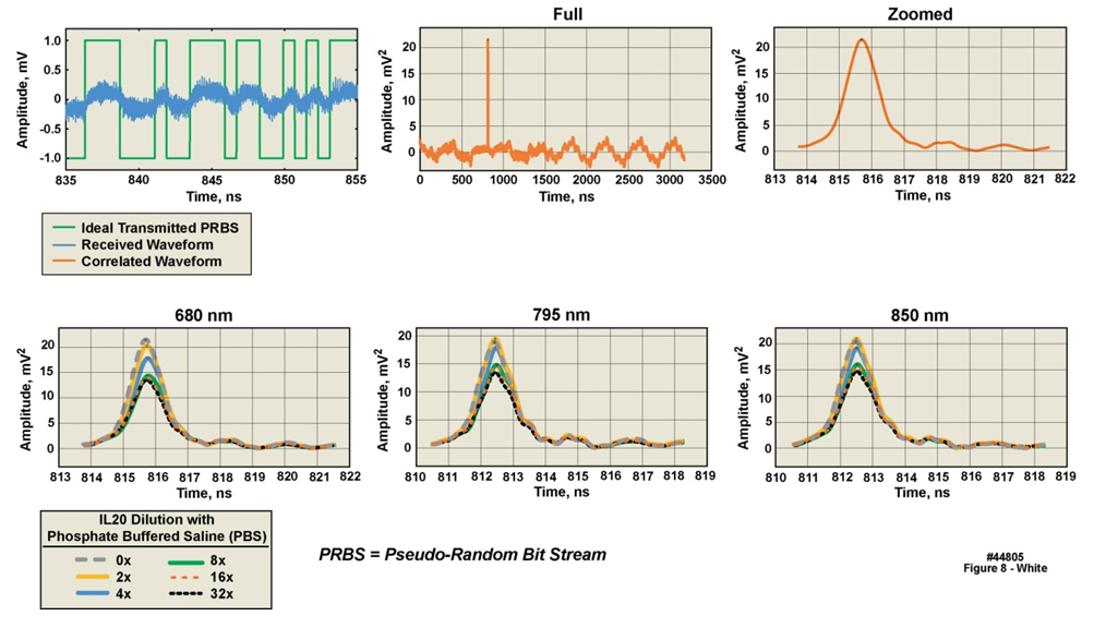 | Figure 8. Lab post-processed waveforms for various dilutions of intralipid-20%. Simultaneous wavelengths are recovered and their responses are displayed. (44805) |
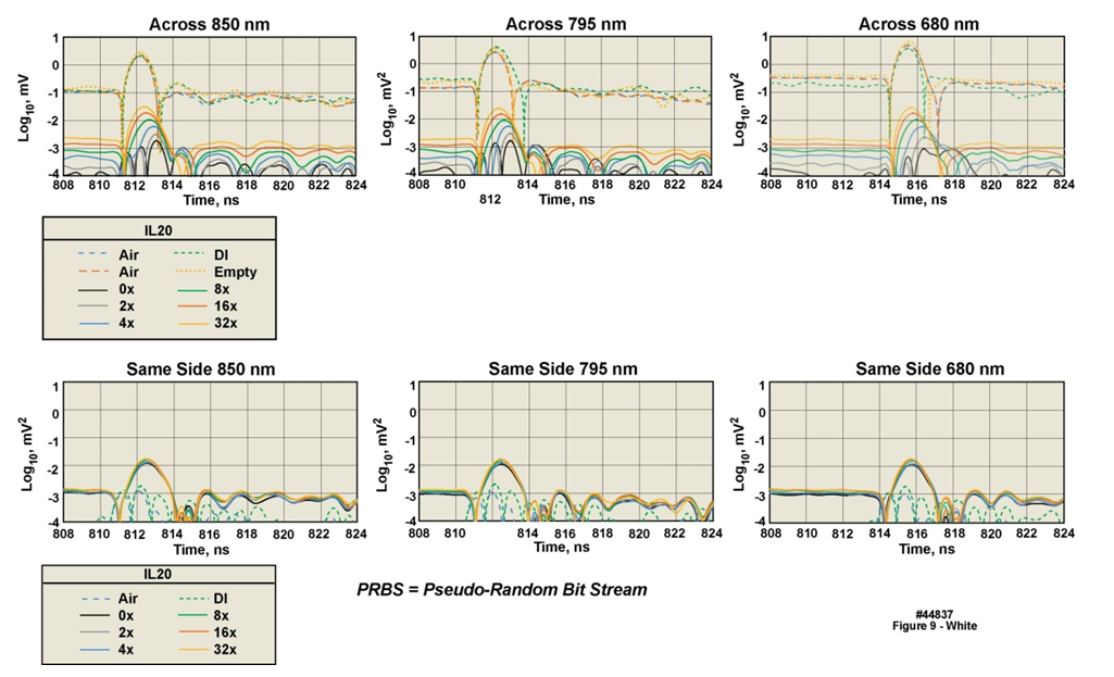 | Figure 9. Comparison of cuvette orientations in lab measurements. Post-processing of the recovered signal shows results for three simultaneous wavelengths. Test medium was intralipid 20% diluted by varying fractions. (44837) |
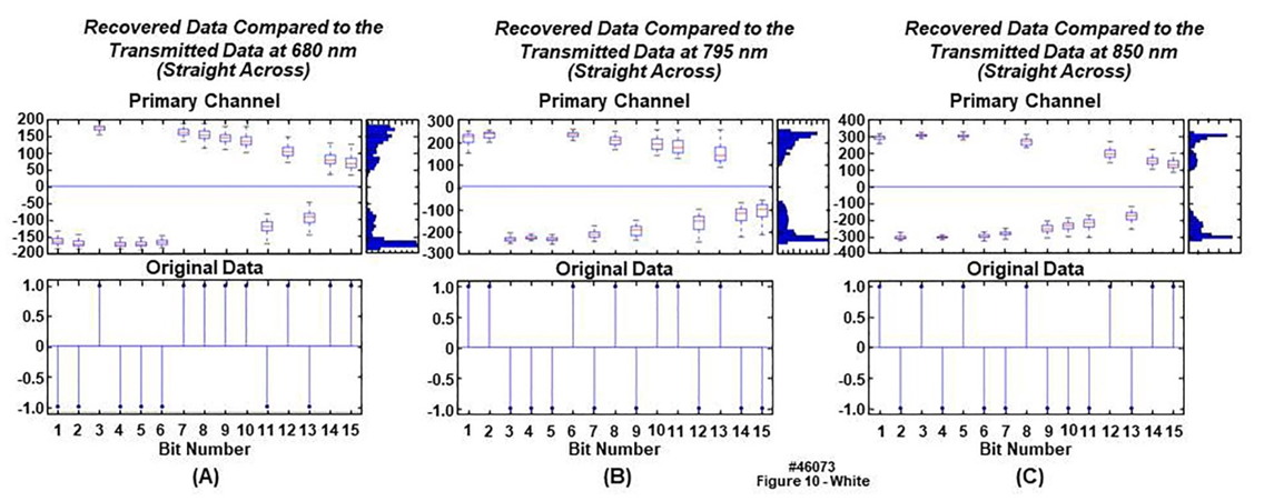 | Figure 10. Data recovery of multiple wavelengths to verify wavelength separation. (46073) |
4. Conclusions
- This paper describes the design and test of analog front ends for multiple wavelength, multiple detector free-space optical measurements. Commodity optical and electrical components were used to construct a compact front-end transmitter and receiver pair. The transmitter demonstrated a tri-wavelength VCSEL solution that had sufficiently fast optical edges and 1-2 mW modulation amplitudes. The receiver demonstrated an APD solution with linear gain stages to supply 50 dB of gain with a bandwidth of 600 MHz. The system was tested with various media. In each case the wavelengths were recovered from small signals through simultaneous measurement and post-processing.
ACKNOWLEDGEMENTS
- The authors would like to thank Shaun Schreiber, Mary Daun-Lindberg, James Bublitz, and Charles Burfield for all of their effort in building and testing this hardware. The authors would also like to thank Drs. Franklin Cockerill, Stefan Grebe and Ravinder Singh for support in this effort.
References
| [1] | M. Moreira et al., "A Low-Cost NIR Digital Photometer Based on InGaAs Sensors for the Detection of Milk Adulterations With Water," in IEEE Sensors Journal, vol. 16, no. 10, pp. 3653-3663, May15, 2016. |
| [2] | M. Renna et al., "Eight-Wavelength, Dual Detection Channel Instrument for Near-Infrared Time-Resolved Diffuse Optical Spectroscopy," in IEEE Journal of Selected Topics in Quantum Electronics, vol. 25, no. 1, pp. 1-11, Jan.-Feb. 2019, Art no. 7201611. |
| [3] | J. Kraitl, U. Timm, H. Ewald and E. Lewis, "Non-invasive measurement of blood components," 2011 Fifth International Conference on Sensing Technology, Palmerston North, 2011, pp. 253-257. |
| [4] | M. N. Ericson et al., "Development of an implantable oximetry-based organ perfusion sensor," The 26th Annual International Conference of the IEEE Engineering in Medicine and Biology Society, San Francisco, CA, 2004, pp. 2235-2238. |
| [5] | N. Hemmati, S. K. Setarehdan and H. Ahmadi Noubari, "Multi-channel Near-Infrared Spectroscopy (NIRS) system for noninvasive monitoring of brain activity," Proceedings of 2012 IEEE-EMBS International Conference on Biomedical and Health Informatics, Hong Kong, 2012, pp. 212-215. |
| [6] | A. W. Lam, "Direct-detection APD-based optical CDMA using orthogonal signalings," [1991 Proceedings] Tenth Annual International Phoenix Conference on Computers and Communications, Scottsdale, AZ, USA, 1991, pp. 513-519. |
| [7] | G. P. Agrawal, "Fiber-Optic Communication Systems, 4th Edition," in Fiber-Optic Communication Systems, 2011. |
| [8] | A. Ishimaru, Wave propagation and scattering in random media, 1997. |
| [9] | N. G. Jerlov, "Optical Oceanography," Elsevier oceanography series, 5, 1968. |
| [10] | F. Xu, M.-A. Khalighi and S. Bourennane, "Impact of Different Noise Sources on the Performance of PIN-and APD-based FSO Receivers," in Proceedings of the 11th International Conference on Telecommunications, 2011. |
| [11] | E. Kamrani, F. Lesage and M. Sawan, "Low-Noise, High-Gain Transimpedance Amplifier Integrated With SiAPD for Low-Intensity Near-Infrared Light Detection," in IEEE Sensors Journal, vol. 14, no. 1, pp. 258-269, Jan. 2014. |
| [12] | D. Milovančev, T. Jukić, B. Steindl and H. Zimmermann, "Optical wireless monolithically integrated receiver with large-area APD and dc current rejection," in 2017 Advances in Wireless and Optical Communications (RTUWO), 2017. |
| [13] | M. Tavakoli, L. Turicchia and R. Sarpeshkar, "An Ultra-Low-Power Pulse Oximeter Implemented With an Energy-Efficient Transimpedance Amplifier," in IEEE Transactions on Biomedical Circuits and Systems, vol. 4, no. 1, pp. 27-38, Feb. 2010. |
| [14] | S. Zahedi and J. A. Salehi, "Analytical comparison of various fiber-optic CDMA receiver structures," Journal of Lightwave Technology, 2000. |
| [15] | W. Guo, X. Sheng, H. Liu and X. Zhu, "Development of a Multi-Channel Compact-Size Wireless Hybrid sEMG/NIRS Sensor System for Prosthetic Manipulation," in IEEE Sensors Journal, vol. 16, no. 2, pp. 447-456, Jan.15, 2016. |