Leila Hajshahvaladi1, Hassan Kaatuzian1, Mohammad Danaie2
1Photonics Research Laboratory (PRL), Department of Electrical Engineering, Amirkabir University of Technology, Tehran, Iran
2Faculty of Electrical and Computer Engineering, Semnan University, Semnan, Iran
Correspondence to: Hassan Kaatuzian, Photonics Research Laboratory (PRL), Department of Electrical Engineering, Amirkabir University of Technology, Tehran, Iran.
| Email: |  |
Copyright © 2017 Scientific & Academic Publishing. All Rights Reserved.
This work is licensed under the Creative Commons Attribution International License (CC BY).
http://creativecommons.org/licenses/by/4.0/

Abstract
In this paper, a simple and non-complex structure for an optical double Bandpass Filter (BPF) based on two-dimensional (2D) Photonic Crystal Ring Resonators (PCRRs) is suggested for ITU-T G.694.2 8-channel Coarse Wavelength Division Multiplexing (CWDM) optical systems. It is centred at wavelengths of 1491 nm and 1551 nm with the aim of minimum attenuation. The desired BPF is composed of a 20×19 square lattice of dielectric rods using semiconductor InAs rods. The normalized transmission spectra simulations and the Photonic Band Gap (PBG) calculations for the desired filter are done using two-dimensional finite-difference time-domain (2D-FDTD) and Plane Wave Expansion (PWE) methods, respectively. The simulation results confirm the normalized output transmission efficiencies, quality factors (Q) and Full Width at Half Maximum (FWHM) for desired BPF are equal to about 99%, 497 and 3 nm (for 1491 nm) and nearly 100%, 310.2 and 5 nm (for 1551 nm), respectively. High transmission efficiencies, acceptable quality factors and low FWHM are important characteristics of proposed filter.
Keywords:
Photonic crystal, Optical filter, Quality factor, CWDM, FDTD, PWE
Cite this paper: Leila Hajshahvaladi, Hassan Kaatuzian, Mohammad Danaie, Analysis and Design of Semiconductor Photonic Crystal Double Bandpass Filter for CWDM Systems, International Journal of Optics and Applications, Vol. 7 No. 3, 2017, pp. 49-54. doi: 10.5923/j.optics.20170703.01.
1. Introduction
Currently some of important purposes of researchers in the field of optical electronics and photonics, are design of photonic crystal (PCs) devices [1]. In recent years, PCs have attracted more attentions, due to having applications in optical electronics, telecommunications and optical information processing [2, 3]. PCs are nanostructures that their dielectric materials refractive indices change periodically. These nanostructures are divided into three principle groups one-dimensional (1D), two-dimensional (2D) and three-dimensional (3D) structures [4]. 2D PCs compared with 1D and 3D PCs have attracted more attentions because they have a complete PBG and also they can be fabricated much easily using integrated circuit technology [5]. PCs are good choices for designing optical filters and other similar elements because of their photonic band gap (PBG) [6-8]. In PC structures, the PBG is a range of frequencies which electromagnetic wave can not be propagated into the structure [9]. In optical communication systems, optical filters are considered vital elements for wavelength division multiplexing (WDM) applications [10, 11]. WDM systems are used in the transmission of information types such as voice, internet, video, and etc. Hence, in optical telecommunication networks one of the ways to increase the capacity of data transmission is by using WDM systems [12]. These systems consist of a multiplexer at the transmitter to combine the optical signals into a single signal and a multiplexer at the receiver to separate the combined signals. In optical telecommunication network, the Coarse Wavelength-Division Multiplexing (CWDM) systems and Dense Wavelength-Division Multiplexing (DWDM) systems are the two patterns for WDM systems. Currently, CWDM systems in comparison with DWDM systems are more attractive because they are low cost. According to the ITU-T G694.2 standard in 8-channel CWDM systems, optical channels are mixed together in the wavelengths range of 1311 nm to 1451 nm (with the aim of minimum dispersion) and 1471 nm to 1611 nm (with the aim of minimum attenuation) with a channel spacing of 20 nm [13]. However, in CWDM systems the important wavelengths are 1471 nm, 1491 nm, 1511 nm, 1531 nm, 1551 nm, 1571 nm, 1591 nm and 1611 nm, which they are corresponding to the ITU-T G.694.2 standard for CWDM systems [14].In this study, one simple and non-complex structure for an optical double Bandpass Filter (BPF) based on two-dimensional (2D) circular Photonic Crystal Ring Resonators (PCRRs) by using a composition of two quasi waveguides and a circular PCRR has been reported. Here the simplest structure geometry that has been used as a basic structure BPF has been designed in Ref. [11]. This structure acts as BPF and cover almost the entire C-band of CWDM systems. The C-band is comprised of the wavelengths in the range of 1530 nm to 1565 nm [11]. Hence in this paper, by applying some changes in the structural parameters of the filter including the radii (r) and the material of dielectric rods, we converted the previous wide BPF (the result of the Ref. [11]) into the narrow double BPF. The resonant wavelengths in our double BPF have been tuned at 1491 nm and 1551 nm. Finite-difference time-domain (FDTD) and Plane Wave Expansion (PWE) methods have been used to calculate the normalized transmission spectra and the photonic band gap of the basic structure, respectively [16]. The rest of this paper is organized as follows: In Section.2, the structure of the proposed BPF is explained. In Section.3, we’ll describe in details the effect of design parameters on filter performance and simulation results. We’ll also have a conclusion section.
2. Single-ring PC Bandpass Filter
The structure used in this study is a 20×19 square lattice photonic crystal of semiconductor InAs material dielectric rods embedded in air substrate. The refractive index of InAs is about 3.5 [17]. We have chosen the radii of the all dielectric rods to be 0.185a, while the lattice constant “a” is set as 530 nm. Our proposed BPF structure is shown in Figure 1.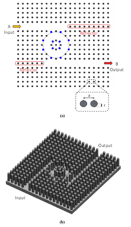 | Figure 1. Schematic structure of double BPF based on circular PCRR (a) 2D view of BPF (b) 3D view of BPF |
Figure 1(a) and (b) depict two-dimensional (2D) and three-dimensional (3D) views of the desired filter, respectively. With respect to Figure 1, the desired BPF comprises of two quasi waveguides (line defects) and a circular PCRR (point defects) between them. In optical filters, the process of selecting wavelengths is performed using the PCRRs [18]. The top quasi waveguide and bottom quasi waveguide are defined as input quasi waveguide and output quasi waveguide, respectively. This structure has two ports. Input port is located in left side of input quasi waveguide and output port in right side of output quasi waveguide. They are labelled as A and B, respectively. As shown in Figure 1, using two circular dotted lines labels, the positions of some dielectric rods have been altered in order to form the circular PCRR. Also, some rods that have been displaced from their previous position in order to compose a circular ring resonator. The reflector rods are placed above the right side of the input quasi waveguide and below the left side of output quasi waveguide, which are used to improve output efficiency of the desired BPF by diminishing counter propagation modes [11].The band diagrams of PC structure without any imperfection in the structure are computed by 2D Plane Wave Expansion (PWE) method. It is represented in Figure 2. There are two PBG regions for transverse magnetic (TM) modes whose magnetic fields are parallel to the dielectric rods. The normalized frequency range of wide PBG (Band gap 1) and narrow PBG (Band gap 2) are between 0.2915 < a/λ < 0.4336 and 0.7268 < a/λ < 0.7506, respectively. Here λ is the wavelength of light in free space. Assuming that the lattice constant “a” is 530 nm, these normalized frequencies ranges are corresponding to the wavelengths range of 1221 nm < λ < 1816 nm and 705 nm < λ < 728 nm, respectively. They are located in the wide PBG (Band gap 1) which covers the optical fiber communications window. Therefore, our proposed filter is suitable for applications in fiber-optic communications.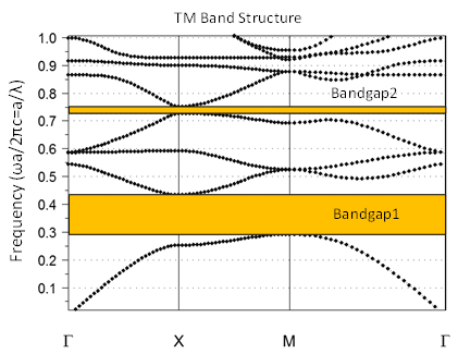 | Figure 2. Band diagram of the basic PC structure for 20×19 square lattice |
When the proper optical signal is applied to the proposed structure through the input port “A”, it passes through the output port “B”. Depending on the wavelength of the input optical signal, it can be guided either to the port B via the ring resonator or it may not drop into the ring resonator and reflect to the port A [19, 20]. A broadband Gaussian pulse is applied into the port “A”. Then, the transmitted spectral power density of the desired BPF is calculated at each output ports. The received spectral power density of the port “B” were normalized to the incident power density from input port “A” [11].
3. Simulation and Results
The normalized transmission spectra at the output port “B” of the proposed double BPF is estimated by calculating Fast Fourier Transform (FFT). The electric (E) and magnetic (H) field components are calculated by two-dimensional (2D) finite-difference time-domain (FDTD) method. In order to obtain an accurate and stable simulation, the spatial mesh must be small enough [13]. Therefore, we consider the FDTD mesh sizes used in the analysis as ∆x=∆z=a/16. Thus, they will be ∆x=∆z=33.125 nm. However, the temporal step size is estimated as follow: | (1) |
Where, c is the speed of the light in free space [9]. The quality factor (Q) is defined as the ratio of the central resonance wavelength to Full Width at Half Maximum (FWHM) value, which is calculated as follows [20, 21]: | (2) |
Where, λ0 is the central wavelength at resonance and ΔλFWHM is the full width at half maximum. Figure 3 represents the normalized transmission and reflection spectra of the double BPF (based on circular PCRR) at port B. The resonant wavelengths of the double BPF are observed at 1491 nm and 1551 nm. The obtained results show, this filter is very suitable for the requirements of ITU-T G.694.2 CWDM communications systems. The normalized output transmission at 1491 nm and 1551 nm are estimated to be close to 99% and 100%. The calculated quality factor (Q) of the corresponding bands is 497 and 310.2, respectively. For calculation of the quality factors, the half power wavelengths have been computed by determining the half power from the Maximum power value [19]. Hence, the half power wavelengths for this proposed double BPF at 1491 nm and 1551 nm wavelengths are obtained as 3 nm (1490 nm to 1493 nm) and 5 nm (1548 nm to 1553 nm), respectively. Generally, there is a trade-off between the enhancement of the transmission efficiency and the reduction of the Q factor [15]. Here our purpose is to have maximum normalized output transmission and maximum Q factor (equal to minimum FWHM). For this purpose, we have chosen an optimum value for radius and refractive index of the dielectric rods. In the following, we intend to investigate the effect of different structural parameters on the output spectrum of the proposed double BPF.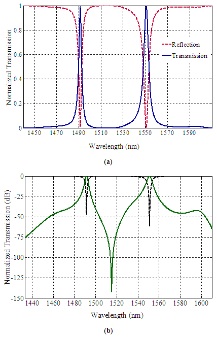 | Figure 3. The normalized transmission and reflection spectra of the proposed double BPF at port B (a) linear scale and (b) dB scale |
First, we investigate the normalized transmission spectra of the proposed double BPF for two bands, by changing the refractive indices (n) values of the dielectric rods. When the change in refractive index is considered, the radius (r=0.185a) and the lattice constant (a=530 nm) parameters are kept constant. The normalized transmission spectra of the proposed filter for two bands for semiconductor InAs (n=3.5) and Si (n=3.4) materials is represented in Figure 4. 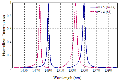 | Figure 4. The normalized transmission spectra of the proposed double BPF for InAs (n=3.5) and Si (n=3.4) materials |
Our investigations show that, by increasing the values of refractive indices, the central wavelengths at resonance of filter is transferred to higher wavelengths [16]. Therefore, it can be set by changing the refractive index value. We consider the highest transmission efficiency at resonant wavelengths 1491 nm and 1551 nm. According to Figure 4, our proposed double BPF of semiconductor InAs material in comparison with Si-type material, has a better performance.Next, we increase the radii (r) of the dielectric rods of the desired double BPF, where their refractive index is 3.5. By changing the radii of the dielectric rods, the filter parameters such as the normalized output transmission and Q factor are affected. The results are shown in Figure 5. It can be observed that, when the radii of the rods are increased, the central wavelengths of the filter are shifted into the higher wavelengths. Therefore, with respect to results, the spectral selectivity and the Q factor of our proposed filter with r=0.185a are higher.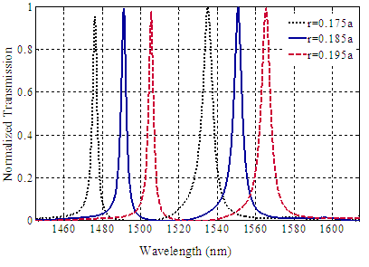 | Figure 5. The normalized transmission spectra of the proposed double BPF for different values of the radii of the dielectric rods (r) |
Tables 1 and 2 present the detailed specifications of the double BPF (based on circular PCRR) for two bands for different values of the radii (r) and the refractive indices (n) of the dielectric rods, respectively. As seen, the best conditions are obtained for the radius of 0.185a and the refractive index of 3.5, while the lattice constant is set as 530nm.Table 1. Simulated Parameters of BPF (Based on Circular PCRR) for InAs and Si materials
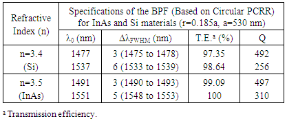 |
| |
|
Table 2. Simulated Parameters of BPF (Based on Circular PCRR) for different values of the radius
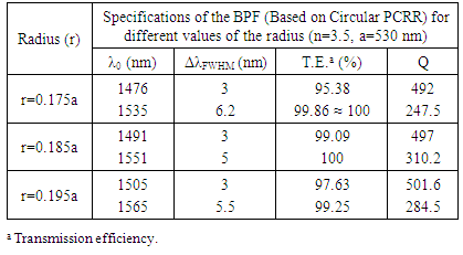 |
| |
|
Finally, in Figure 6, we investigate the effect of the lattice constant (a) on the operation of the proposed double BPF for two bands, while the radius (r=0.185a) and the refractive index (n=3.5) parameters are kept constant. Figure 6 represents the normalized transmission spectra of the proposed double BPF for different values of the lattice constant. By increasing the lattice constant, the normalized output transmission and Q factor are not changed significantly, however the central wavelengths are transferred to higher wavelengths. As seen in Figure 6, by changing the lattice constant of structure, we’ll have a double BPF with acceptable performance in the important wavelengths of the CWDM systems, so that they are corresponding to the ITU-T G.694.2 standard. 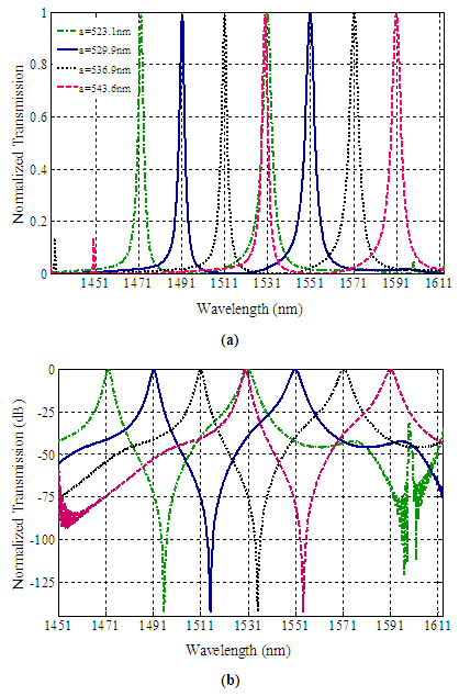 | Figure 6. The normalized transmission spectra of the proposed double BPF for different values of the lattice constant (a) linear scale and (b) dB scale |
Figures 7(a), (b) and (c) represent the distribution of the electric field inside the structure for the desired double BPF at port B for three different wavelengths such as 1491 nm, 1551 nm and 1510 nm, respectively. Figures 7(a) and (b) show that at resonant wavelengths λ=1491 nm and λ=1551 nm, the optical waves (electric fields) are fully coupled to the circular PCRR and transmit towards port B, whereas according to Figure 7(c), in non-resonance wavelength λ=1510 nm, the optical wave will not be directed to the port B.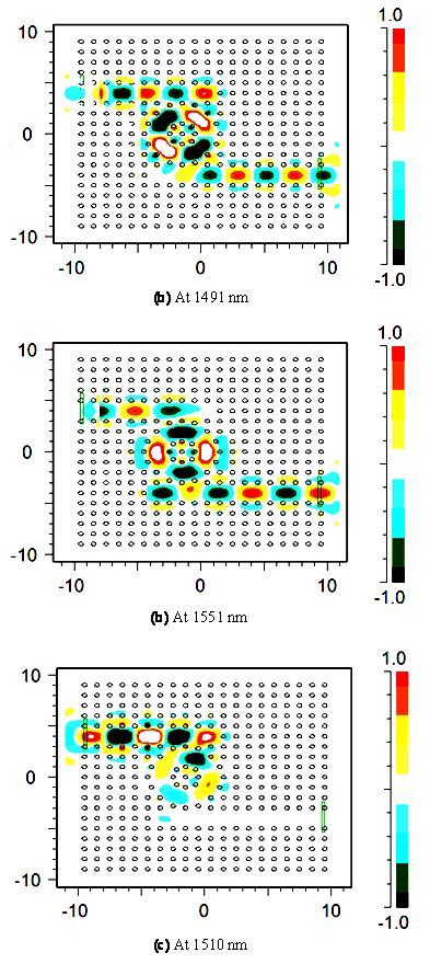 | Figure 7. The distribution of the electric field inside the structure for proposed double BPF at port B for wavelengths of (a) 1491 nm (b) 1551 nm (c) 1510 nm |
4. Conclusions
In this study, one simple and non-complex structure for an optical double BPF based on 2D circular PCRRs has been reported for CWDM optical systems. The BPF is centred at resonant wavelengths of 1491 nm and 1551 nm with the aim of minimum attenuation. The structure used in the BPF design is 20×19 square lattice of semiconductor InAs material dielectric rods embedded in air substrate. The simulation results demonstrate that the normalized output transmissions at wavelengths 1491 nm and 1551 nm (with the aim of minimum attenuation) are estimated to be close to 99% and 100% with calculated Q factors of 497 and 310.2, respectively. Generally, there is a trade-off between the enhancement of the transmission efficiency and the reduction of the Q factor. Our investigation shows that, by increasing the value of design parameters such as the refractive indices, radii of the rods and lattice constant, the resonant wavelengths are transferred to higher wavelengths values. Therefore, the resonant wavelengths of filter can be set by changing these parameters values. The proposed structure may be more useful for CWDM systems and metro networking applications.
References
| [1] | Kaatuzian H., “Photonics, Vol.2”, 3’rd printing, AKU Press 2017. (in Persian) |
| [2] | Danaie, M. and H. Kaatuzian, Bandwidth improvement for a photonic crystal optical Y-splitter. Journal of the Optical Society of Korea, 2011. 15(3): p. 283-288. |
| [3] | Benmerkhi, A., M. Bouchemat, and T. Bouchemat, Design of Photonic Crystal Demultiplexer for Optical Communication Application. Nanoscience and Nanotechnology, 2016. 6(1A): p. 29-34. |
| [4] | Danaie, M. and H. Kaatuzian, Design and simulation of an all-optical photonic crystal AND gate using nonlinear Kerr effect. Optical and Quantum Electronics, 2012. 44(1-2): p. 27-34. |
| [5] | Moghaddam, M.K., M.M. Mirsalehi, and A.R. Attari, A 60° photonic crystal waveguide bend with improved transmission characteristics. Optica Applicata, 2009. 39(2). |
| [6] | Deghdak, R., et al., Optimized complete photonic band gap in magneto-photonic crystal slab. Nanoscience and Nanotechnology, 2016. 6(1A): p. 39-42. |
| [7] | Arafa, S., et al., Design of Optical Filter Based on Photonic Crystal Squared Silicon Nitride Microcavity. Nanoscience and Nanotechnology, 2016. 6(1A): p. 97-104. |
| [8] | Bendjelloul, R., et al., New Design of T-Shaped Channel Drop Filter Based on Photonic Crystal Ring Resonator. Nanoscience and Nanotechnology, 2016. 6(1A): p. 13-17. |
| [9] | Rezaee, S., M. Zavvari, and H. Alipour-Banaei, A novel optical filter based on H-shape photonic crystal ring resonators. Optik-International Journal for Light and Electron Optics, 2015. 126(20): p. 2535-2538. |
| [10] | Kiaee, M.S. and F.E. Seraji, Design of a 32× 5 Gb/s DWDM Optical Network over a Distance of 1000 km. International Journal of Optics and Applications, 2016. 6(2): p. 31-36. |
| [11] | Robinson, S. and R. Nakkeeran, PCRR Based Bandpass Filter for C and L+ U Bands of ITU-T G. 694.2 CWDM Systems. Optics and Photonics Journal, 2011. 1(03): p. 142. |
| [12] | Akhavan, A., H.G. Fard, and V. Varmazyari, Dynamically-Tunable Terahertz Band-Stop Filter Based on Multilayer Graphene Metamaterial. International Journal of Optics and Applications, 2017. 7(1): p. 7-12. |
| [13] | Robinson, S. and R. Nakkeeran. Add drop filter for ITU-T G. 694.2 CWDM systems. in Electronics Computer Technology (ICECT), 2011 3rd International Conference on. 2011. IEEE. |
| [14] | Mahmoud, M.Y., G. Bassou, and F. Metehri, Channel drop filter using photonic crystal ring resonators for CWDM communication systems. Optik-International Journal for Light and Electron Optics, 2014. 125(17): p. 4718-4721. |
| [15] | Qiang, Z., W. Zhou, and R.A. Soref, Optical add-drop filters based on photonic crystal ring resonators. Optics express, 2007. 15(4): p. 1823-1831. |
| [16] | Benelarbi, D., T. Bouchemat, and M. Bouchemat, Design of High-Sensitive Refractive Index Sensor Using a Ring-Shaped Photonic Crystal Waveguide. Nanoscience and Nanotechnology, 2016. 6(1A): p. 105-109. |
| [17] | Herve, P. and L. Vandamme, General relation between refractive index and energy gap in semiconductors. Infrared physics & technology, 1994. 35(4): p. 609-615. |
| [18] | M. Danaie and H. Kaatuzian, “Photonic Crystals, Innovative Systems, Lasers and Waveguides", edited by A. Massaro, Chpt.8, INTECH Publisher, 2012. |
| [19] | Sathyadevaki, R. and A.S. Raja, Design of dual ring wavelength filters for WDM applications. Optics Communications, 2016. 380: p. 409-418. |
| [20] | Sathyadevaki, R., D.S. Sundar, and A.S. Raja, Diagonally coupled hexagonal photonic crystal filter for optical supervisory channel. 2016. |
| [21] | L. Hajshahvaladi, H. Kaatuzian, M. Danaie, “Design and Simulation of Infrared Photonic Crystal Bandpass filters for Fiber Optics Communications", accepted and presented in ICEE-2017 conference, May 2017. |

 Abstract
 Reference
 Full-Text PDF
 Full-text HTML