-
Paper Information
- Paper Submission
-
Journal Information
- About This Journal
- Editorial Board
- Current Issue
- Archive
- Author Guidelines
- Contact Us
International Journal of Optics and Applications
p-ISSN: 2168-5053 e-ISSN: 2168-5061
2017; 7(1): 7-12
doi:10.5923/j.optics.20170701.02

Dynamically-Tunable Terahertz Band-Stop Filter Based on Multilayer Graphene Metamaterial
Ali Akhavan1, Hassan Ghafoori Fard1, 2, Vali Varmazyari1
1Department of Electrical Engineering, Amirkabir University of Technology, Tehran, Iran
2Photonics Engineering Group, Amirkabir University of Technology, Tehran, Iran
Correspondence to: Hassan Ghafoori Fard, Department of Electrical Engineering, Amirkabir University of Technology, Tehran, Iran.
| Email: |  |
Copyright © 2017 Scientific & Academic Publishing. All Rights Reserved.
This work is licensed under the Creative Commons Attribution International License (CC BY).
http://creativecommons.org/licenses/by/4.0/

In this paper, a dynamically-tunable band-stop filter based on periodically patterned graphene nanostrip and nanodisk in THz wavelength is proposed and numerically investigated at room temperature. The properties of proposed structure are calculated by using the finite-difference time-domain method. The patterned graphenes are excited by the incident light which leads to absorb two different ranges of spectral wavelength. The simulated results show that a wide free spectral range can be achieved by using multilayer graphene. More importantly, it is found that the transmission dips can be dynamically controlled by adjusting the gate voltage. Moreover, the transmission dips change with graphene mobility which corresponds to graphene intrinsic loss. Finally, the proposed metamaterial structure may be used for many applications such as tunable sensors, active plasmonic switches, and slow light devices.
Keywords: Graphene Plasmonics, Band Stop Filter, Terahertz Metamaterial, FDTD Method
Cite this paper: Ali Akhavan, Hassan Ghafoori Fard, Vali Varmazyari, Dynamically-Tunable Terahertz Band-Stop Filter Based on Multilayer Graphene Metamaterial, International Journal of Optics and Applications, Vol. 7 No. 1, 2017, pp. 7-12. doi: 10.5923/j.optics.20170701.02.
Article Outline
1. Introduction
- The Terahertz (THz) range of the electromagnetic spectrum has been explored for a wide variety of applications including biomolecular sensing, wireless communication, spectroscopy and etc. [1-3]. Many natural materials do not react to the THz radiation, therefore the THz waves are not most commonly used in comparison with other waves. Whereas, metamaterials, which are artificially made by scientists, can be used in THz range [4]. The optical properties of metamaterial such as periodicity and dielectric properties, let us to control and manage the THz waves and devices [5, 6]. For these reasons, many types of research have been numerically investigated based on metamaterials at THz range [7-9]. Designing of THz devices are one of the common approaches in metamaterials that have active control over the plasmon resonance. It causes that materials were built which have dynamic optical properties such as liquid crystal and nonlinear media [10, 11]. Unfortunately, the refractive index changes of these materials are low by applying mechanical forces and electrical biases. Therefore, the active plasmonic devices that are built with these materials, show low optical performances such as high energy consumption, high plasmonic loss, and low operation speed. Graphene is composed of a single layer of carbon atoms arranged in a two-dimensional hexagonal pattern which has emerged as fascinating material with extraordinary properties such as high electron mobility, flexibility and etc. [12-15]. Plasmonic devices based on graphene guide surface plasmon modes with low loss which can be dynamically tuned by changing the electrostatic doping [16, 17]. These unique properties are a suitable candidate to be used in tunable and compact plasmonic devices. Recently, many devices have been theoretically and experimentally studied such as active plasmonic switching with graphene ribbon arrays [18], Fano metamaterial with tuning of the electrical properties of graphene for switching and sensing applications [19], tunable infrared plasmonic devices with graphene/insulator stacks [20], switching terahertz waves with gate-controlled graphene metamaterials and electromagnetic response [21] and broadband ultrafast dynamics of few-layer epitaxial graphene [22].In this paper, a tunable band-stop filter with periodic structure consists of nanostrip and nanodisk graphenes. Two patterns of graphene are excited by the incident wave at the same time and absorb two different spectrum wavelengths. The surface conductivity of single-layer graphene is modeled which can be used to simulate the device performance by using the finite difference time-domain (FDTD) method. Then, structure geometry of proposed tunable band-stop filter is presented. After that, important geometric parameters of structure and graphene are considered in order to investigate the filter transmission spectra. Finally, the performance of presented device is investigated in optical telecommunication application, especially in optical switching.
2. Graphene Surface Conductivity Model
- In this section, the properties of graphene surface conductivity are introduced. A complex surface conductivity is used for modelling of graphene. The surface conductivity contains intra-band and inter-band transitions. At the THz range, it can be calculated with random phase approximation, according to Kubo formula [23]:
 | (1) |
 | (2) |
 | (3) |
 in which μ is dc mobility and vF=106 m/s (Fermi velocity in graphene) [19]. Also, the reported model can be used for multilayer graphene. In the multilayer graphene, the surface conductivity is achieved by scaling the conductivity in number of layers in equation (1) [20, 24]. Actually, graphene mobility depends on its preparation method. In previous reports, μ=230000 cm2/V.s has been experimentally achieved in suspended graphene [25]. High value of graphene mobility on SiO2 substrate has been reported μ=40000 cm2/V.s [26]. In recent researches, the combination of hexagonal boron nitride (h-BN) and graphene have been introduced, which can improve electrical properties of graphene. Because h-BN has a few surface trapped charges which has only 1.8 % lattice mismatch with graphene [27]. In the simulation, the device performance is assumed at room temperature, and µ=10000 cm2/V.s.
3. Structure Geometry and Simulation Method
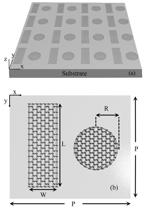
- Figure 1(a) illustrates the conceptual schematic of designed graphene plasmonic band-stop filter. The geometry of unit cell is depicted in figure 1(b). The patterned graphene is deposited on the substrate of silicon dioxide with relative permittivity 2.09. The unit cell has a square lattice with period array P=1 µm. The radius of graphene nanodisk is R=200 nm, also the length and width of graphene strip have been assumed L=600 and W=150 nm, respectively. A normally incident y-polarized wave (i.e., the electric field component parallel to y-direction) is used for excitation of surface plasmon modes [28].
 is obtained from S-parameters, and the field distribution is calculated by frequency-domain field profile monitor in 5nm above graphene layers.
4. Results and Discussions
- The transmission spectra of graphene nanostructure is presented in figure 2(a) that shows, the first and second dips are appeared at frequencies of 9.07 and 15.81 THz, respectively. Also, figure 2(b) shows the phase of transmission spectra. As demonstrated in this figure, the surface plasmon polariton (SPP) modes are generated in graphene nanostructures. The first and second dips are corresponded to graphene nanostrip and graphene nanodisk, respectively. The z-component of electric field at two dip frequencies are shown in figure 2(c) and 2(d).
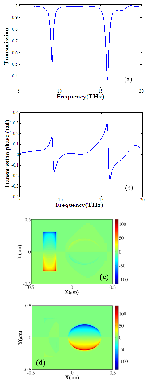 | Figure 2. (a) The transmission spectra of the proposed filter. (b) The phase of transmission spectra. (c), (d) z-component of electric field at 9.07 THz and 15.81 THz |
 | (4) |
 Figure 3 demonstrates the transmission spectra with different values of graphene nanostrip length. As can be seen that, by increasing the nanostrip length, the resonance frequency and transmission intensity at the first dip are decreased because the coupling strength is increased.
 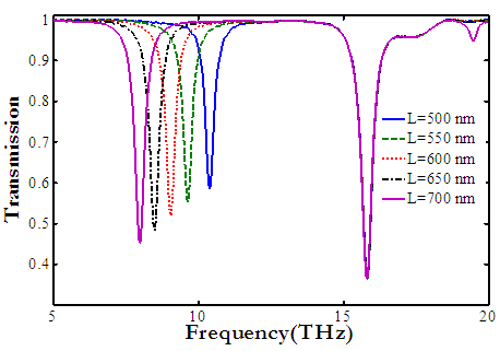 | Figure 3. The transmission spectra with different values of graphene nanostrip length L |
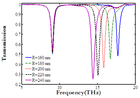 | Figure 4. The transmission spectra with different values of graphene nanodisk radius R. The Fermi level energy is 0.6 eV |
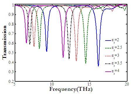 | Figure 5. The transmission spectra with different values of substrate permittivity εr |
 the resonance frequency can be tuned by applied voltage [29]. Where Vapp and t are the applied voltage between gating pad and substrate, and thickness of substrate, respectively. Figure 6 shows the obtained transmission spectra of proposed structure under different values of µc. It can be clearly seen that the resonance frequencies are gradually blue-shifted with the increase of µc. Furthermore, the blue-shift of transmission spectra can be justified by the equation (4).
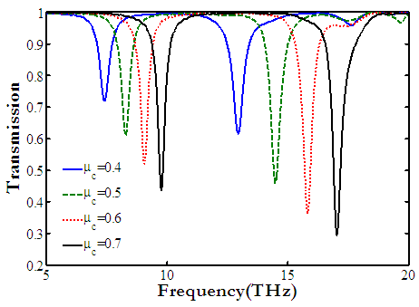 | Figure 6. The transmission spectra with different values of graphene Fermi level energy µc |
 Figure 7 shows the transmission spectra for one, two and three layers of graphene. By increasing the number of layers, the resonance frequencies are increased and the transmission dips are became smaller. This property can be used for many applications such as sensors. It can be seen that, the difference between two resonance frequencies are enlarged by increasing the number of layers, it means that, free spectral range (FSR) is increased. FSR in one, two and three layers of graphene are 6.75 THz, 9.46 THz and 11.46 THz, respectively. Finally, the influence of electron mobility
  is considered on performance of proposed filter which correspond to graphene intrinsic loss. The transmission spectra for four values of mobility is shown in figure 8. For low mobility µ (high loss), the transmission efficiency is decayed. For actual values of mobility near
  the efficiency of device is desirable.
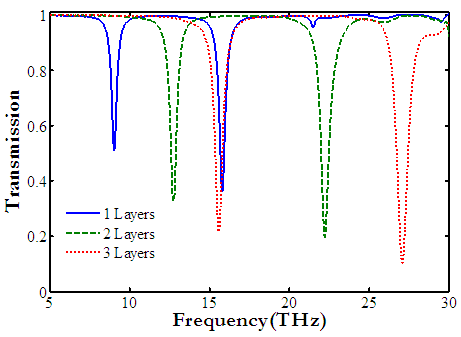 | Figure 7. The transmission spectra of N-layer graphene, N=1,2,3 |
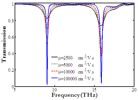 | Figure 8. The transmittance of nanostructure for different values of mobility µ |
5. Design a Switch Based on Graphene Metamaterial
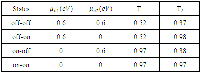
- In the suggested device, the transmission spectra has been changed by modifying the structure geometry and properties of graphene. Therefore, it can be used for many applications such as optical telecommunication, especially in optical switching. To investigate optical switching performance, the relevant parameters in the presented structure are selected by values of P=1 µm, L=600 nm, W=150 nm, R=200 nm, εr=2.09 and µ=10000 cm2/V.s. Also, by adjusting the Fermi level energy in two patterns of graphene, the proposed device can be operated as an optical switch at two resonance frequencies of 9.05 THz and 15.81 THz. The values of Fermi level energy are listed in table 1. The Fermi level energy of nanostrip and nanodisk are μc1 and μc2, respectively.
|
 | (5) |
 and
and  are the magnitude of transmittance at the "on" and "off" states, respectively. The MD for first resonance frequency is 0.48 and second resonance frequency is 0.64. As can be seen in figure 8, for increasing MD, the graphene with high mobility (low loss) can be used.Figures 9(a) - 9(d) show the transmission spectra of the proposed switch at all states. In figure 9(a), when μc1=0.6 eV and μc2=0.6 eV, two dips are appeared and the switch sets in off state. As shown in Figures 9(b) - 9(c), by setting the appropriate values of μc1 and μc2, the switch is adjusted in "on" state for one of two frequencies. Figure 9(d) shows that the switch is "on" state and all wavelengths are transmitted in which μc1=0 eV and μc2=0 eV.
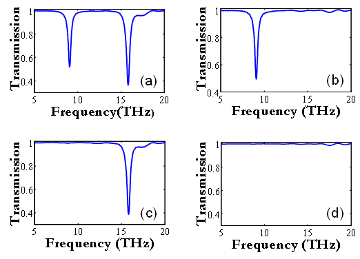 | Figure 9. Transmittance of the switch at different states: (a) μc1=0.6 eV and μc2=0.6 eV, (b) μc1= 0.6 eV and μc2=0 eV, (c) μc1=0 eV and μc2= 0.6 eV and (d) μc1=0 eV and μc2=0 eV |
6. Conclusions
- In summary, we proposed a dynamically tunable terahertz band-stop filter based on multilayer graphene metamaterial. The graphene metamaterial consists of disk and strip structures. The influences of substrate permittivity and structure parameters on the resonance frequencies and transmission dips were studied in details by FDTD method. The results exhibited that the resonance frequencies can be slightly shifted by adjusting the applied voltage between gating pad and substrate. The effect of graphene layers on the performance of proposed filter was studied. Finally, a switch was proposed for optical telecommunication application, in which the transmission dips are controlled by Fermi level energy. Fortunately, the proposed structure can be fabricated with latest mico-nano fabrication technologies.
 Abstract
 Reference
 Full-Text PDF
 Full-text HTML