-
Paper Information
- Paper Submission
-
Journal Information
- About This Journal
- Editorial Board
- Current Issue
- Archive
- Author Guidelines
- Contact Us
International Journal of Optics and Applications
p-ISSN: 2168-5053 e-ISSN: 2168-5061
2015; 5(4): 133-146
doi:10.5923/j.optics.20150504.04
Modeling and Analysis of a Miniaturized Ring Modulator Using Silicon-Polymer-Metal Hybrid Plasmonic Phase Shifter. Part II: Performance Predictions
 Abstract
 Reference
 Full-Text PDF
 Full-text HTML
Alhuda A. Al-Mfrji1, Shelan K. Tawfeeq1, Raad S. Fyath2
1Institute of Laser for Postgraduate Studies, University of Baghdad, Iraq
2College of Engineering, Al-Nahrain University, Iraq
Correspondence to: Raad S. Fyath, College of Engineering, Al-Nahrain University, Iraq.
| Email: |  |
Copyright © 2015 Scientific & Academic Publishing. All Rights Reserved.
The ring modulator described in part I of this paper is designed here for two operating wavelengths 1550nm and 1310nm. For each wavelength, three structures are designed corresponding to three values of polymer slot widths (40, 50 and 60nm). The performance of these modulators are simulated using COMSOL software (version 4.3b) and the results are discussed and compared with theoretical predictions. The performance of intensity modulation/direct detection short range and long rang optical communication systems incorporating the designed modulators is simulated for 40 and 100Gb/s data rates using Optisystem software (version 12). The results reveal that an average energy per bit as low as 0.05fJ can be obtained when the 1550nm modulator is designed with a phase shifter length equals twice the coupling length.
Keywords: Ring modulator, Hybrid plasmonic phase shifter, Electro-Optic polymer
Cite this paper: Alhuda A. Al-Mfrji, Shelan K. Tawfeeq, Raad S. Fyath, Modeling and Analysis of a Miniaturized Ring Modulator Using Silicon-Polymer-Metal Hybrid Plasmonic Phase Shifter. Part II: Performance Predictions, International Journal of Optics and Applications, Vol. 5 No. 4, 2015, pp. 133-146. doi: 10.5923/j.optics.20150504.04.
Article Outline
1. Performance of the 1550nm Modulators
- This section presents simulation results for three
 ring modulators designed with different polymer slot widths
  . The design methodology presented in Part I of this paper is used to find the corresponding values of silicon waveguide width that makes the real parts of the effective indices of the photonic mode and plasmonic mode equal and hence ensuring phase matching between the two modes. The refractive indices of silicon, silica, and silver used in the simulation are 3.48 [1], 1.44, and 0.15 + j11.5 [2], respectively. The electro-optic (EO) organic material used in the simulation is Carbazole-Phenoxy based Methacrylate homopolymer. The refractive index of the polymer is characterized by
  at zero applied voltage and an EO coefficient
  of
of  . The common geometric parameter values used to simulate the three modulators are silicon waveguide height
  , polymer slot height
  , and height of silica space between silicon waveguide and plasmonic waveguide
  .
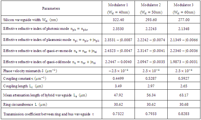
.1.1. Modulator Structure Parameters Deduced from the Simulation
- Table 1 lists the individual parameter values obtained via simulation for the three modulators. Few remarks about Table 1 are given here refractive indices of these two modes are complex and denoted here by
 and
and  , respectively. (i) The silicon-plasmonic hybrid phase shifter behaves as a directional coupler where two eigen modes (quasi-odd and quasi-even modes) will be excited when the hybrid phase shifter is driven by the input photonic mode. The effective (ii) The phase velocity mismatch between the photonic mode and plasmonic mode δ and the coupling constant characterizing the virtual hybrid phase shifter coupler
  are calculated using the relations
  and
and 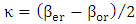 [3] where
  is the propagation constant of the photonic mode,
 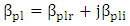 is the propagation constant of the metal-dielectric-metal (MDM) plasmonic mode (
 is the vacuum propagation constant). Further, the propagation constants of the quasi-even and quasi-odd modes are given, respectively, by
 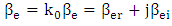 and
and 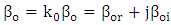 .(iii) The coupling length between the photonic and plasmonic waveguides is estimated using the relation
 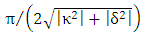 . Note that the three modulators are characterized by
  which indicates perfect velocity match between the photon mode (in silicon waveguide) and the plasmonic mode (in the MDM waveguide). (iv) The length of the hybrid phase shifter
  is set equals to
  to ensure high transfer of power from the plasmonic mode to the photonic mode at the end of the phase shifter.(v) The ring circumference
  is set initially to
  in the design and then tuned slightly to ensure a resonance wavelength of 1550nm via simulation for each of the designed modulators.(vi) The mean attenuation length of the hybrid wavelength
  is computed as
  .(vii) The simulation results reveal that the roundtrip loss of the
  silicon waveguide section in the racetrack is about 0.18dB. Thus the loss factor
 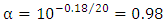 . For each designed modulator, the length of the coupler section between the waveguide bus and the microning is tuned to achieve a critical coupling that satisfies
 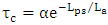 .
.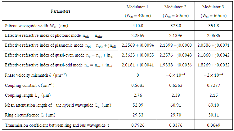 | Table 1. Parameter values obtained via simulation for the three 1550nm modulators |
1.2. Performance Results
1.2.1. Phase Matching Condition
- The phase matching between photonic and plasmonic modes is satisfied for different polymer slot widths
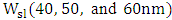 as represented by points A, B, and C in Fig. 1. The corresponding values of silicon waveguide width
  are 410,373 and 351.8nm, respectively.
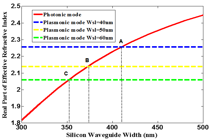 | Figure 1. Real part of the effective refractive indices of photonic and plasmonic modes as a function of silicon waveguide width W_si for different polymer slot widths of 40nm, 50nm, and 60nm |
1.2.2. Electric Field Distribution
- The electric field (Ex) profiles for photonic mode, plasmonic mode, quasi-even mode, and quasi-odd mode are depicted in Fig. 2 for the modulator designed with
 . The modulator is excited by 1550nm optical signal under zero applied voltage. It can be seen that the electric fields in the plasmonic arm are much stronger than those in dielectric arm. For the quasi-even eigen mode, the electric field orientation in the two arms are the same while they become opposite in the quasi-odd eigen mode.
  | Figure 2. Electric field distribution for photonic (a), plasmonic (b), quasi-even (c), and quasi-odd (d) modes associated with  modulator operating at 1550nm and zero applied voltage modulator operating at 1550nm and zero applied voltage |
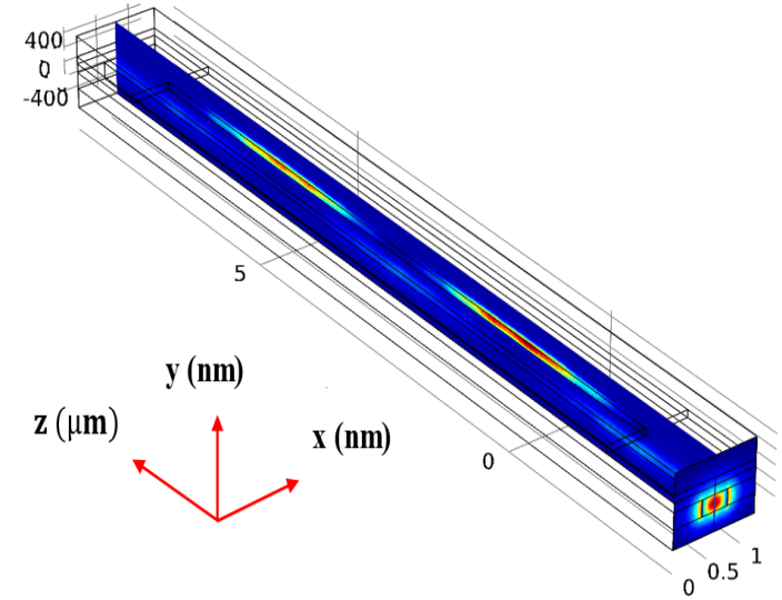 | Figure 3. 3D simulated electromagnetic energy density distribution for the 50nm-width polymer slot at 1550nm photonic mode excitation |
 | Figure 4. Energy density distribution in the hybrid phase shifter for the three modulators under zero applied voltage   |
1.2.3. Coupling Characteristics of the Silicon-Plasmonic Coupler
- Figure 5 provides clear picture for the power transfer characteristics between the silicon waveguide and plasmonic slot waveguide as a function of interaction length
 (from
(from  to
to  , where
  is the phase shifter length). The results are presented for the three modulators under zero applied voltage. Due to the presence of losses, the variation of the power in each waveguide with propagation distance
  has a damped sinusoidal behavior. As z increases, the field transfers from the silicon waveguide to the plasmonic waveguide (and vice versa) gradually owing to the interference of the quasi-even mode and quasi-odd mode. Investigating the results in this figure reveals that at
  , 66%, 74%, and 78.5% of the incident power is transmitted to the of the power silicon waveguide arm when
  , and 60nm, respectively.
 | Figure 5. Dependence of output power from the two hybrid coupler arms on the interaction length z when the field is fed from the silicon arm for three modulators designed with 40 (a), 50 (b) and 60nm (c) slot widths |
1.2.4. Extinction Ratio and Insertion Loss
- The simulation is carried further to investigate the extinction ratio
 and insertion loss
  of the three ring modulators and the results are depicted in Figs. 6 and 7, respectively. Figure 6 displays the transmission characteristics versus wavelength for two values of applied voltage
  , 0 and 1V. Note that the 1V-applied voltage shifts the resonance frequency from 1550nm to 1550.38nm, 1550.23nm, and 1550.18nm (red shift) for the 40nm, 50nm, and 60nm slot width modulators, respectively. The corresponding extinction ratio (insertion loss) are 51.4dB (20.0dB), 46.0dB (21.8dB), 41.0dB (230.5dB), respectively.
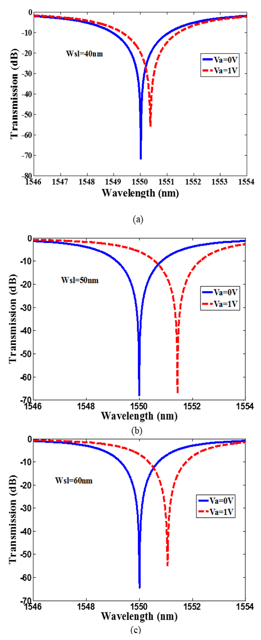 | Figure 6. Transmission spectra of the three designed modulators under 0 and 1V applied voltages.  |
 and
and  are almost symmetric around zero voltage. An extinction ratio of
  is achieved when
  for three modulators.
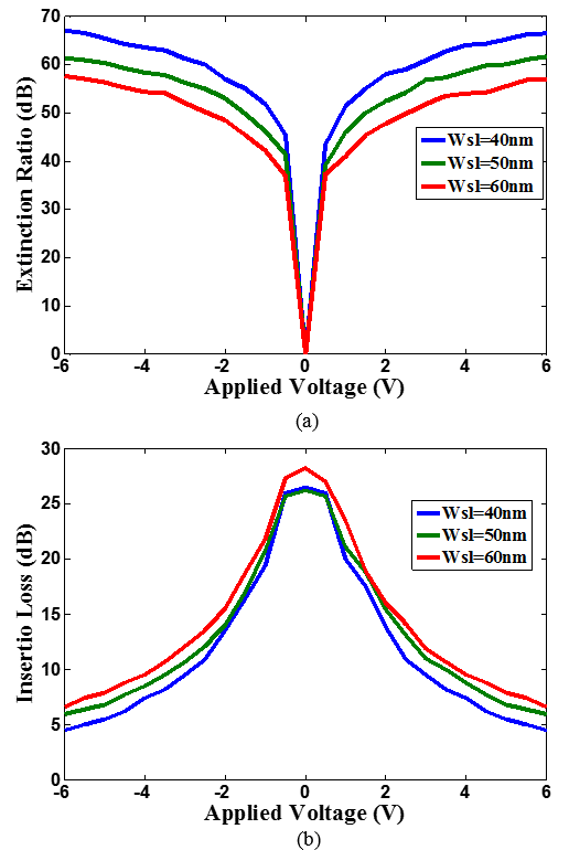 | Figure 7. Extinction ratio (a) and insertion loss (b) as a function of the applied voltage for the three 1550nm modulators |
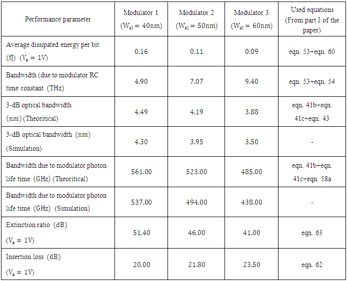
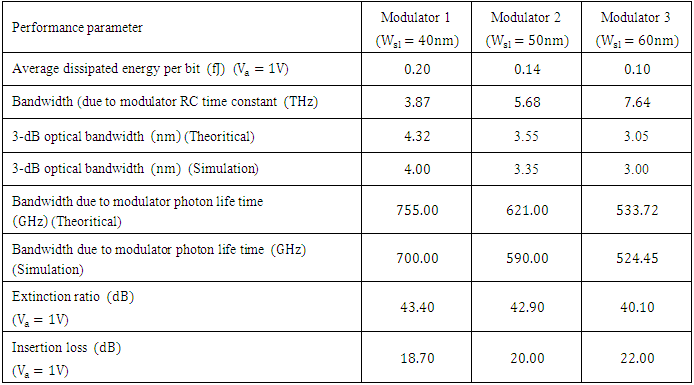
1.2.5. Performance Comparison of the Designed Modulators
- The performance of three modulators are compared and results are summarized in Table 2. Performance parameters that depends on the applied voltage is calculated at
 . Investigating the results in this table highlights the following findings(i) The three modulators are characterized by high extinction ratio (more than 40dB). Recent experimental demonstration of high bit rate optical communication systems indicate that optical modulators with extinction ratio as low as
  satisfy the requirement [4-6].(ii) Bandwidth due to photon life time
  dominates the modulator bandwidth. The modulator bandwidth is 485, 523, and 561 GHz for slot width 40, 50, and 60nm, respectively. Note that the three modulators are designed with almost the same value of
  . Therefore, the decrease in modulator bandwidth comes from the effect of the critical coupling
  (see eqn. (57b) in Part I of this paper).(iii) The average dissipated energy per bit
  decreases with increasing
  . According to eqn. (60) given in Part I of this paper,
  is directly proportional to the modulator capacitor. For the three modulators under investigation, the energy per bit is proportional to
  since the slot height is the same for three devices. Note further
  decreases slightly as
  increases (see Table 1). Thus assuming that
  depends linearly only on
  will slightly under estimate the modulation bandwidth.(iv) Theoretical predictions are in good agreement with simulation results.
|
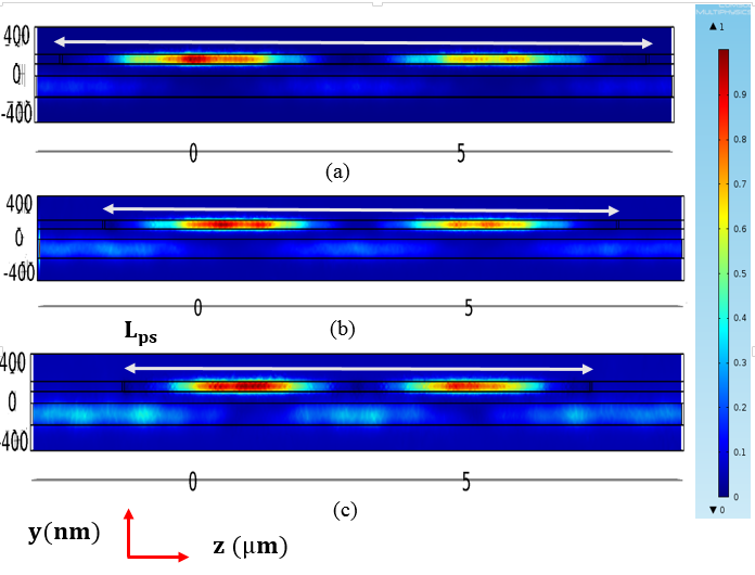
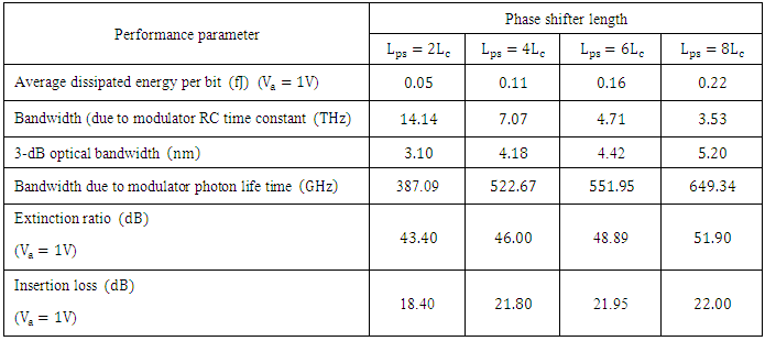
1.2.6. Effect of Phase Shifter Length
- In the previous subsections, the simulation results have been presented for ring modulators designed with a hybrid phase shifter having a length equals four times the coupling length (i.e.,
 ). In this subsection, performance comparison among ring modulators designed with different phase shifter lengths are addressed. Four modulator structures having
  and
and  are designed and simulated for 1550nm operation with
  . Note that the phase shifter lengths
  are even number of the coupling length in all the four structures and hence satisfy maximum power transfer for the plasmonic waveguide to the silicon waveguide at the end of the phase shifter.Mode analysis is performed for the hybrid phase shifters in the four structures using COMSOL software and the results reveal that the modal characteristics of the plasmonic and photonic modes are not affected by the length of the phase shifter. The reason behind that is the cross section dimensions and the materials of the phase shifter structure are the same for the four modulators. The modal simulation ends with
  and
and  for these devices.Figure 8a-d show the field distribution in the hybrid phase shifter when
  and
and  , respectively. Note that when
  increases, the peak of the energy density decreases at the last part of the phase shifter due to the losses associated with the plasmonic waveguide.
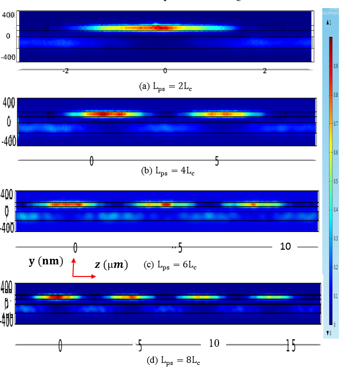 | Figure 8. Energy density distribution in the hybrid phase shifter for the four modulators under zero applied voltage and 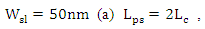  |
 for
for 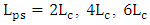 and
and  , respectively. The corresponding critical coupling
  obtained via simulation is 0.9060, 0.8376, 0.7742, and 0.7156, respectively.Table 3 lists the main performance parameters of the four structures under investigations. These results can be explained by noting that increasing the phase shifter length will increase both cavity loss and modulator capacitance (the latter is directly proportional to
  ). Investigating the results in Table 3 highlights the following findings(i) The insertion loss is almost independent of phase shifter length and this effect is more pronounced when
  .(ii) The extinction ratio increases slightly
  as the phase shifter length increases by
  .(iii) The bandwidth due to modulator RC time constant
  is inversely proportional to the phase shifter length. Note that
  is inversely proportional to modulator capacitance and hence inversely proportional to the phase shifter length.(iv) The average dissipated energy per bit
 increases linearly with
  due to the modulator capacitance effect.
  increases from
  to
to  as
as  increases from
  to
to  .(v) The cavity photon lifetime decreases with increasing
  due to the increase of associated loss. Therefore, the bandwidth due to photon lifetime increases with increasing
  .
.  increases from
  to
to  as
as  increases from
  to
to  .
.
|
2. Performance of 1310nm Ring Modulator
- Three ring modulators are designed for 1310nm operation using different polymer slot widths (40, 50, and 60nm). The refractive indices of silicon, silica, and silver at 1310nm are set to 3.5193 [1], 1.44621 and 0.09+j8.828 [2]. Unfortunately, the refractive index and EO coefficient of Carbazole-Phenoxy based Methacrylate homopolymer are not reported in the literature at 1310nm wavelength. Therefore, the same values adopted in the 1550nm design are used here. It is worth to mention here that the EO coefficient
 of polymers generally increases when wavelength decreases [7, 8]. The values of geometric parameters that are common for the three structures are silicon waveguide height
  , polymer slot height
  , and the height of silica space between silicon waveguide and plasmonic waveguide
  . Thevalues of these three dimensions are identical to those used in the 1550nm design.The ring circumference L and the transmission coefficient between the bus waveguide and the ring
  are tuned to achieve 1310nm resonance wavelength and critical coupling, respectively, for each designed modulators. Table 4 lists the geometric and physical parameters obtained via simulation when the phase shifter length
  equals four times the coupling length
  . Performance parameters of the modulators are summarized in Table 5. The results in the table highlights the following findings(i) For a specific value of polymer slot width
  , the ratio
 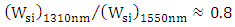 for three values of
  considered here (40, 50, and
  ). Note the ratio between the two wavelengths is
  Thus the normalized silicon waveguide width
  is almost the same for both operating wavelengths when
  is fixed. It is worth to mention here that in microwave and millimeter wave engineering, the geometric dimensions of the designed devices are usually expressed in a normalization form with respect to wavelength. This is useful to obtain a universal design which can be configured according to the required operating wavelength. This statement seems to be also applicable for the designed modulators where
  scales with wavelengths ratio. However, the effective wavelength ratio
  rather than 0.845 since the other silicon waveguide dimensions are kept the same for both wavelength designs.(ii) Recall that the coupling length
 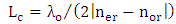 . At fixed value of
  , the ratio
 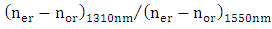 is approximately around
  . This leaves
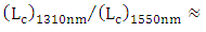
 which is good agreement with results reported in the table.(iii) Since the modulators are designed with
  , then
 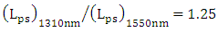 . The modulator capacitance will increase by the same ratio,
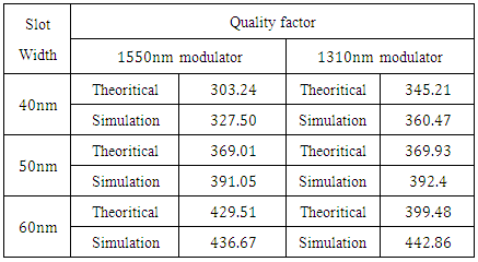
 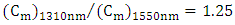 . This yields an increase in the average energy per bit and a decrease in the modulator bandwidth due to RC time constant by 1.25 when one moves from 1550nm to 1310nm design.(iv) The quality factor
  does not vary much for the two modulators designed at 1310nm and 1550nm resonance wavelength when
  is fixed (see Table 6). This leaves the modulator bandwidth due to photon lifetime
 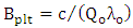 is determined mainly by
  . Thus
 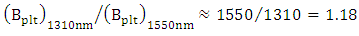 . This is in accord with average ratio of 1.2 estimated from both simulated and calculated bandwidth values, listed in Tables 2 and 5.(v) The 1310nm modulators are characterized by relatively lower extinction ratio and insertion loss compared with the 1550nm counterpart.
|
|
|
3. Performance of Optical Communication Systems Incorporating the Designed Modulators
- The aim of this section is to address the performance of short-reach and long-reach intensity modulation/direct detection (IM/DD) optical communication systems incorporating the designed ring modulators. The intensity modulation uses the electrical signal (information) to modulate the optical carrier at the transmitter while direct detection uses a photodiode to recover the information from the received modulated carrier without using local laser at the receiver side. Recently, there is increasing interest to use IM/DD technique in optical networks. For example, to provide ever-increasing user rates at limited costs of infrastructure deployment, IM/DD systems coupled with the use of a single-mode fiber (SMF) widely installed all around the orderare preferred [9]. Further, for short-reach 100Gb/s applications, IM/DD is seen as more practical than coherent modulation/detection techniques implemented in long-haul optical communication systems [10]. High bit rate IM/DD short reach communication has been demonstrated successfully at both 1550nm [11, 12] and 1310nm [13, 14]. The 1550nm and 1310nm corresponds to minimum loss wavelength and zero-dispersion wavelength of standard SMF.The simulation results represented in this section are obtained using Optisystem ver. 12 which is a commercially software package used to simulate optical communication systems. The results are given for 1310nm and 100Gb/s IM/DD binary communication system operating as a single channel at 1550nm or 1310nm. Electronic modulator driving circuits that support binary 40Gb/s modulation have been already being used in installed high speed optical communication systems [15, 16]. However, extensive research are going on different international laborites to design electronic systems to support 100Gb/s operation [17].To reflect the effect of the three modulator bandwidth components into the simulation, the binary data is passed through a three-stage of a first-order RC filter. Each filter uses a
 resistance with a capacitance calculated to yield the required bandwidth component according to
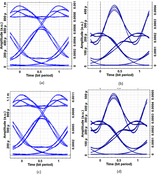
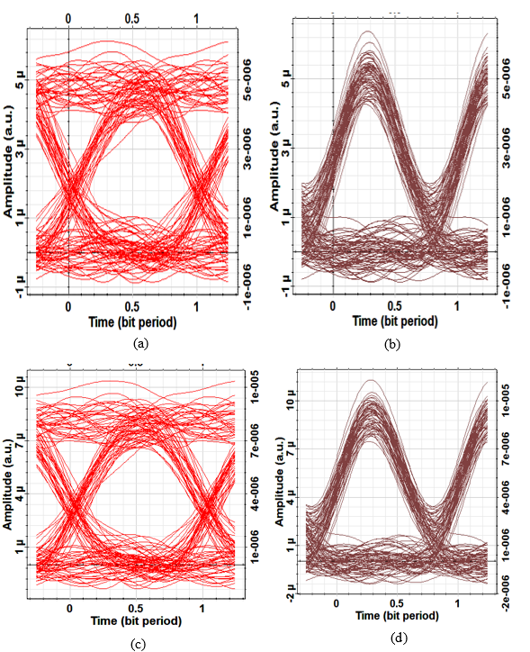
  . The bandwidth of the driving circuit is set equal to 0.75 of the bit rate.Figures 9a and 9b show the transmitter eye diagrams corresponding to 40Gb/s nonreturn-to-zero (NRZ) and 50% return-to-zero (RZ) signaling, respectively, at 1550nm operation. Results related to 100Gb/s are given in Figs. 9c and 9d. No DC (bias) voltage is applied to the modulator while the binary data voltage is 0V for logic Zero and 1V for logic One.
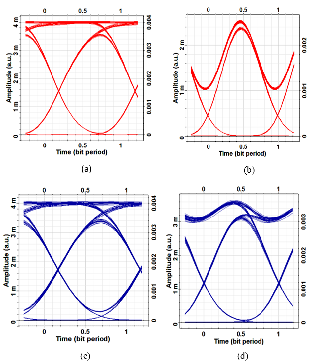 | Figure 9. Transmitter eye diagrams at 1550 nm operation for   |
3.1. Long-Reach Optical Communication System
- In general, this communication system relies heavily on the deployed long-haul optical communication links and operates at 1550nm. The dispersion and losses of these links are generally compensated using dispersion compensated fibers (DCFs) and optical amplifiers (OAs), respectively. Figure 10 shows a block diagram for the long-reach optical communication system under investigation. The link consists of
 identical spans. Each span contains a 80km SMF, with
 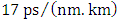 2nd-order dispersion
  and
and  loss
loss  , and a
  DCF having dispersion
 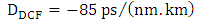 and loss
  . Note that the average 2nd-order dispersion of the span
 which indicates that the span is dispersionally compensated. (Here
  and
and  are lengths of the SMF and DCF sections, respectively). An optical amplifier is also inserted after each fiber section to compensate its losses and hence spans with zero average loss are obtained. An optical bandpass filter, with optical bandwidth equals twice the receiver electrical bandwidth, is also inserted at the end of the transmission link to reduce the amount of accumulated amplified spontaneous emission generated by optical amplifiers that incident at the photodiode. An optical amplifier is also placed right of the modulator which acts as a power booster amplifier to compensate the modulator losses. Other parameter values used in the simulation are listed in Table 7.
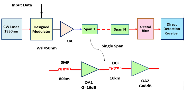 | Figure 10. Long-reach optical communication system. The insert gives the components of a single span |
|
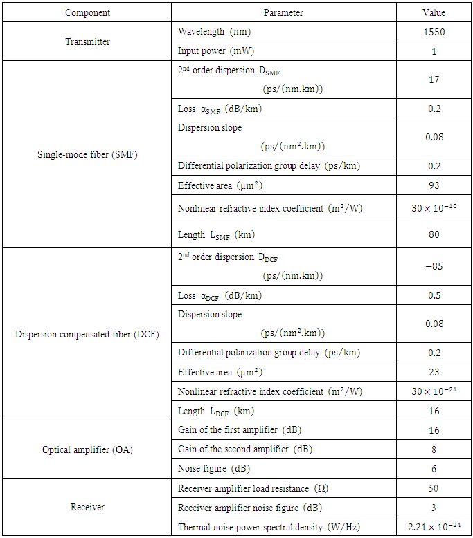
 , the number of spans
  should be less than 9, 11, 5, and 4, respectively.
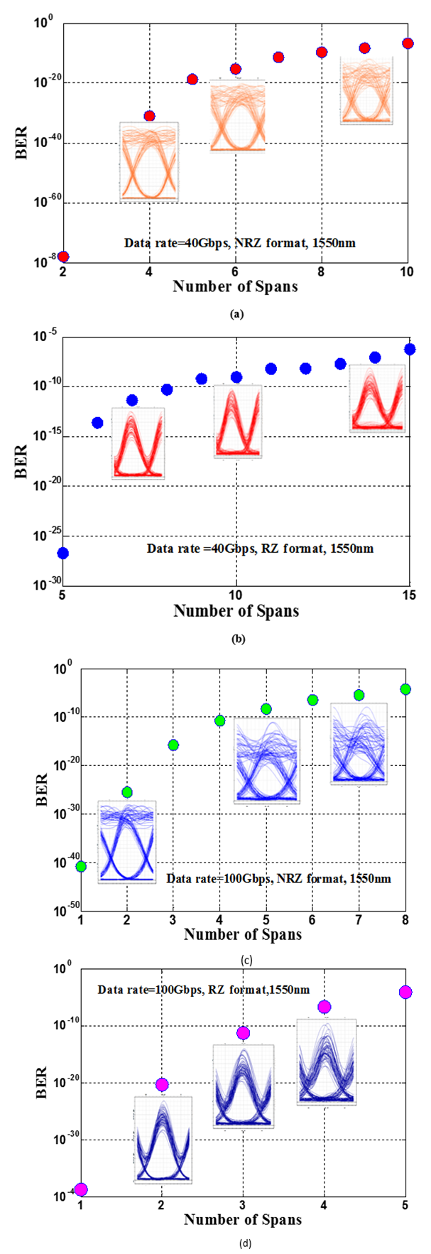 | Figure 11. Dependence of BER on number of spans for 40Gb/s NRZ (a), 40Gb/s RZ (b), 100Gb/s NRZ (c), and 100Gb/s RZ (d) |
3.2. Short-Reach Optical Communication System
- This subsection examines the performance of a short-reach system incorporates the designed modulators along with a SMF connecting the transmitter with receiver. From cost point of view, no DCF or OA is used to compensate the fiber dispersion and link losses, respectively.Two modulators are considered in the simulation, one is designed for 1550nm operation and the other for 1310nm operation, both with slot width=50nm. At the 1310nm, the second-order dispersion of the SMF is approximately zero and therefore one should take the effect of the third-order dispersion through the dispersion slope
 .Table 8 lists the maximum allowable transmission distance that yields a BER
  . Results are reported for 40 and 100Gb/s bit rates, NRZ and RZ signal format, and 1550 and 1310nm operation.
|
 in short reach optical communication system
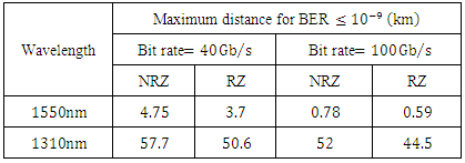
 | Figure 12. Receiver eye diagrams for 1550nm short-reach operation with 40Gb/s NRZ (a), 40Gb/sRZ (b), 100Gb/sNRZ (c), and 100Gb/s RZ (d) |
 | Figure 13. Receiver eye diagram for 1310nm short-reach operation with 40Gb/s NRZ (a), 40Gb/s RZ (b), 100Gb/s NRZ (c), and 100Gb/s RZ (d) |
4. Conclusions
- Performance predictions have been presented for plasmonic ring modulators designed for 1550nm and 1310nm wavelengths. The key role played by polymer slot width and the length of the hybrid phase shifter have been identified in detail. An extinction ratio more than 40dB is obtained at 1V applied voltage for both operating wavelengths. The average energy per bit is about 0.05fJ(0.1fJ) when the 1550nm (1310nm) modulator is designed with phase shifter length equals two times the coupling length of the virtual hybrid coupler covering the interaction between photonic mode and plasmonic mode in the phase shifter.
ACKNOWLEDGMENTS
- The authors would like to thank the anonymous reviewers for their valuable comments and suggestions to improve the quality of the paper. The work is a part of a PhD research program in the Institute of Laser for Postgraduate Studies, University of Baghdad, Iraq. One of the authors, Mrs. Al-mfrji, wishes to thank the College of Engineering at Al-Nahrain University, Baghdad, Iraq, for offering her the PhD scholarship.