-
Paper Information
- Paper Submission
-
Journal Information
- About This Journal
- Editorial Board
- Current Issue
- Archive
- Author Guidelines
- Contact Us
International Journal of Optics and Applications
p-ISSN: 2168-5053 e-ISSN: 2168-5061
2015; 5(4): 121-132
doi:10.5923/j.optics.20150504.03
Modeling and Analysis of a Miniaturized Ring Modulator Using Silicon-Polymer-Metal Hybrid Plasmonic Phase Shifter. Part I: Theoretical Framework
Alhuda A. Al-mfrji1, Shelan K. Tawfeeq1, Raad S. Fyath2
1Institute of Laser for Postgraduate Studies, University of Baghdad, Iraq
2College of Engineering, Al-Nahrain University, Iraq
Correspondence to: Raad S. Fyath, College of Engineering, Al-Nahrain University, Iraq.
| Email: |  |
Copyright © 2015 Scientific & Academic Publishing. All Rights Reserved.
This paper presents comprehensive analysis and investigation for 1550nm and 1310nm ring optical modulators employing an electro-optic polymer infiltrated silicon-plasmonic hybrid phase shifter. The paper falls into two parts which introduce a theoretical modeling framework and performance assessment of these advanced modulators, respectively. In this part, analytical expressions are derived to characterize the coupling effect in the hybrid phase shifter, transmission function of the modulator, and modulator performance parameters. The results can be used as a guideline to design compact and wideband optical modulators using plasmonic technology.
Keywords: Ring modulator, Hybrid plasmonic phase shifter, Electro-Optic polymer
Cite this paper: Alhuda A. Al-mfrji, Shelan K. Tawfeeq, Raad S. Fyath, Modeling and Analysis of a Miniaturized Ring Modulator Using Silicon-Polymer-Metal Hybrid Plasmonic Phase Shifter. Part I: Theoretical Framework, International Journal of Optics and Applications, Vol. 5 No. 4, 2015, pp. 121-132. doi: 10.5923/j.optics.20150504.03.
Article Outline
1. Introduction
- Silicon-based photonic integrated circuits (PICs) are an attractive solution for next generation high-speed data transmission [1, 2]. Usually these circuits are realized using standard complementary metal-oxide semiconductor (CMOS) fabrication technology [3, 4] where silicon photonics offer low cost, low power consumption, and high bandwidth [2]. Recently silicon PICs have been demonstrated for both intra- or inter chip -link, and long haul telecommunication links [2]. Optical interconnects have recently emerged as promising solution for alleviating the bandwidth in modern computing electronics [5]. As a key part of optical interconnect on silicon chips, electro-optic (EO) modulators have been made great progress in recent years and attracted many interests [6]. In addition to that, optical networks have been growing up and integrated components such as optical modulators are widely developed and employed as key components for such application. Especially, the next generation optical networks are demanded to have the features of high capacity, high-speed and high- agility which require the aggregate carrier data per optical fiber to be extended toward 100 Tb/s [7]. This requires high performance modulators capable to deal with ultrahigh speed data rate of single-channel optical signals (100 Gb/s and higher in the future compared with current 10 and 40 Gb/s) [7, 8].Conventional CMOS-compatible silicon optical modulator are usually realized using the linear EO (Pockels) effect rather than carrier depletion effect in order to achieve high speed operation [9-11]. Unfortunately, these modulators suffer from two main limitations(i) CMOS compatibility sets limit to the required operating voltages [6]. Silicon is characterized by relatively low linear EO coefficients and hence requires relatively high modulating voltages. This problem has been solved by incorporating polymer with higher EO coefficient in the active region of the modulator leading to silicon-polymer hybrid modulators [12-15].(ii) Advances in CMOS technology enable the fabrication of integrated electronics on nano-scale size. In contrast, the size of a conventional optical modulator is in order of operating wavelength or higher. A technology emerging recently which can scale down the dimensions of optical devices far beyond the diffraction limit is plasmonics [16]. This technology is based on surface plasmon polariton (SPP) which travels through a form of hybrid electrical/optical propagation [17-19]. A plasmon is a quasi-particle formed from the coupling of a photon and a travelling electron density wave at the interface between a metal and a dielectric [20]. Recently, plasmonic technology has been used to realize ultra-compact modulators suitable for integration with electronic components and hence meet footprint and efficiency requirement of PICs [21].Several ultra-compact plasmonic modulators have been proposed in the literature for 50 Gb/s (and above) operation using silicon-metal [6, 22, 23] or silicon-polymer-metal hybrid structures [11, 24, 25]. The proposed modulators have been designed using Mach-Zehnder interference (MZI) [10, 22, 25-30], nonresonant (forward) waveguide [9, 15, 31-34], or microring resonator (MRR)-based structure [35-37]. Plasmonic modulator for high-level modulation have been also proposed using a combination of MZI and waveguide topologies [11-13]. The microring resonator attracts increasing interest as a promising photonic device for integrated optical interconnects and novel photonic architectures which can be implemented easily in silicon photonic platforms. The main advantages of this device are(i) It can be configured either as an optical modulator or a wavelength division multiplexing drop filter [38].(ii) It offers smaller footprint than the Mach-Zehnder modulator (MZM) [16].(iii) When fabricated using silicon-on-insulator (SOI) platforms, the microning resonator exhibits a great potential to build space, power, and spectrally efficient on-chipphotonic networks that could be seamlessly integrated with CMOS electronics [39].(iv) The microning modulator exhibits smaller chip size and capacitance, resonant-enhanced efficiency, and high wavelength selectively in comparison to MZM [39].(v) When compared to MZM, ring resonator has the potential for low power consumption and array integration [40]. Unfortunately, the performance of MRRs is very sensitive to the operating wavelength, due to their high thermal sensitivity, and to the geometric and material parameter variations, due to their small size. Therefore, the design of microning modulators should be addressed carefully.Recently, Xu et al. [36, 37] have proposed a race track ring-based optical modulator employing an EO polymer infiltrated silicon- plasmonic hybrid phase shifter. Their simulation results reveal a 15dB extinction ratio under 1.2V.This paper presents comprehensive analysis and detailed performance investigation for this modulator structure when it is designed to operate at optical telecommunication wavelengths. The results can be used as a guideline to design ultra-compact and high speed plasmonic modulator suitable for implementation in CMOS platform. The first part of this paper constructs the theoretical framework required to design the modulator and develops general expressions to assess its performance. Simulation results related to modulator performance and its capability to be implemented in high bit rate optical communication systems are given in part II.The simulation results stand heavily on COMSOL 4.3b and partially on OptiSystem 12 software packages.
2. Device Description and Design Methodology
- The silicon-plasmonic racetrack modulator proposed in [36, 37] will be investigated in this paper. This modulator consists of racetrack resonator coupled to a bus waveguide as shown in Fig. 1. The plasmonic slot waveguide with EO organic cladding material is positioned above one of the straight arms (silicon waveguide) of the resonator. This principle is similar to directional coupling between two waveguides. The plasmonic photonic hybrid directional coupler consists of two arms. The upper arm is silver-polymer-silver plasmonic slot waveguide while the lower arm is silicon dielectric waveguide embedded in silicon di-oxide. Different widths of silicon waveguide are obtained according to phase matching condition corresponding to different polymer slot widths.
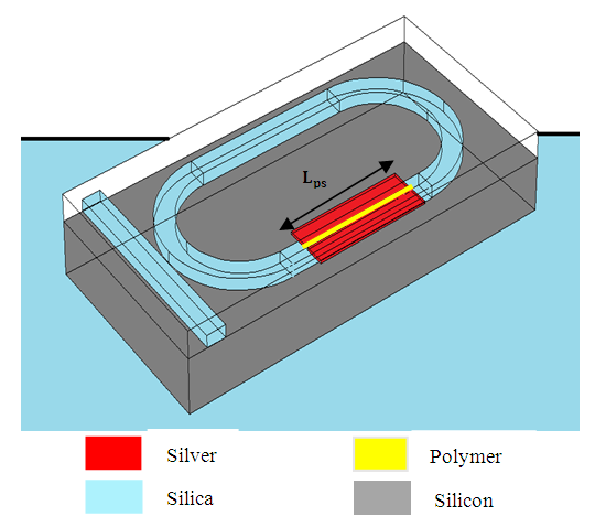 | Figure 1. Structure of Silicon-plasmonic racetrackresonator modulator |
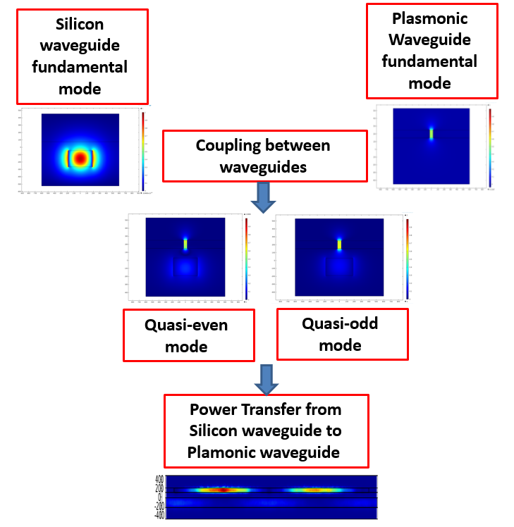 | Figure 2. Basic principle of plasmonic photonic hybrid coupler |
 via Pockels effect, where
  is the modulating voltage and
  is polymer slot width. The refractive index of the polymer is changed by
  , where
  is EO coefficient,
  is the polymer refractive index, and
  is the optical confinement factor of the slot. By modulating the refractive index of the polymer in the slot, the information is encoded in the phase of the SPP.To design the hybrid phase shifter, some important factors should be taken into account.(i) Phase matching condition: The real part of the effective refractive index of the fundamental photonic mode should be equal the real part of the effective refractive index of the fundamental plasmonic mode. This condition is satisfied for a specific polymer slot width as represented by the operating point A in Fig. 3. Thus the required silicon waveguide width
  is obtained. Note that the effective index of the plasmonic mode is independent of
  .
.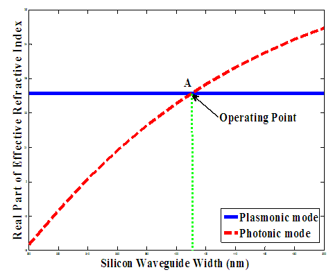 | Figure 3. Real parts of the effective refractive indices of photonic and plasmonic modes as a function of silicon waveguide width |
 . Here
  and
and  represent propagation constants for the quasi-even and quasi-odd modes, respectively.
3. Coupling between Silicon and Plasmonic Waveguides
- The coupling between the modes of plasmonic waveguide and silicon waveguide can be investigated using the concept of parallel two-waveguide coupler as shown in Fig. 4. Both waveguides are assumed to be homogeneous along the direction of propagation (i.e., z axis) with refractive index distribution which is in general a function of x and y axes.
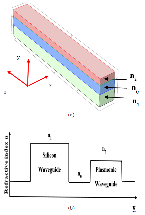 | Figure 4. (a) Parallel two-waveguide coupler model to characterize the interaction between plasmonic and silicon waveguides. (b) Refractive index distribution in the transverse plane of the coupler |
 | (1) |
 | (2a) |
 | (2b) |
 | (3) |
 and
and  are introduced to take into account the coupling effects along the axial direction of the waveguide. The electric field of the propagating wave in the coupler strucure should obey the scalar wave equation
  | (4) |
 is the electrical field complex amplitude,
  is the Laplacian operator, c is the speed of light in vacuum, and
  | (5a) |
 | (5b) |
 | (5c) |
 and
and  obey the orthogonality since they refer to separate transverse regions
 | (6) |
 The transverse behavior of the field in a waveguide can be described by using the wave equation [42, 43]
 | (7) |
 is the transversal Laplacian operator. Therefore, the individual coupler waveguides modes satisfy these equations
 | (8a) |
 | (8b) |
 | (9) |
 | (10) |
 and
and  , respectively, and integrating over the entire xy plane yields two-coupled mode equations
 | (11a) |
 | (11b) |
 | (12a) |
 | (12b) |
 represents the permitivity of vacuum.The coupling constants
  and
and  represent only a small correction to the propagation constants
  and
and  , respectively. The terms with
  and
and  in eqn. (11) result from the dielectric perturbations to one of the waveguide dueto the presence of the other waveguide. Under the assumption that the individual waveguides modes are locallized almost totally in its waveguide, then according to eqn. (12b) one can set
  These leaves eqns. (11a) and (11b) with two coupling constants
  and
and  which form a complex conjugate
  . Under this assumption, eqns. (11a) and (11b) can be rewritten as
 | (13a) |
 | (13b) |
 is assumed to be real without loss of generality and set equals to κ.
 Then
Then | (14a) |
 | (14b) |
 | (15a) |
 | (15b) |
 Then
Then  | (16a) |
 | (16b) |
 | (16c) |
 | (16d) |
 and
and  if the possible values of q obey the following dispersion relation (obtained by setting the determinant of the cofficient matrix to be zero)
 | (17) |
 Dividing eqn. (16a) by (16b) yields
  This gives
 | (18a) |
 | (18b) |
 | (18c) |
 and recall that
  give
give | (19a) |
 yeilds
 | (19b) |
4. Design Concepts of the Plasmonic Ring Modulator
- Based on Fig. 5, the linear input-output relationship of the bus-ring coupler can be described by the matrix relation
 | (20) |
 Straight-through coupling coefficient between bus and ring waveguide.
  Cross-coupling coefficient between bus waveguide and ring waveguide.
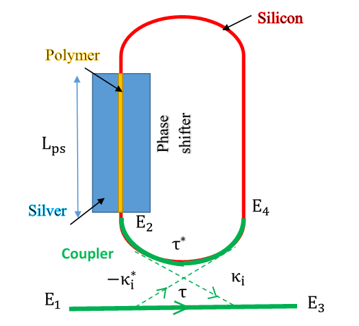 | Figure 5. Model of single racetrack resonator with hybrid phase shifter and one bus waveguide |
 | (21) |
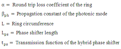 From eqn. (21)
 | (22) |
 | (23a) |
 | (23b) |
 | (24) |
 | (25) |
 is the electric field concentrated on silicon waveguide consisting the hybrid phase shifter. By using coupled mode theory between plasmonic waveguide and silicon waveguide and setting the plasmonic feild
  yields
 | (26) |
 is the mean attenuation length of the hybrid waveguide
  . Here
  is the imaginary part of the effective refractive index of the plasmonic mode
  .The transmission function of the hybrid phase shifter can be written as
 | (27a) |
 | (27b) |
 is the phase velocity mismatch between the silicon waveguide photonic mode and the metal-dielectric-metal (MDM) plasmonic mode [37]
 | (28a) |
 is the propagation constant of the silicon waveguide mode whose effective index
  is assumed to be real (lossless waveguide). Further,
  is the real part of the complex propagation constant of the MDM plasmonic mode
 | (28b) |
 is the complex effective index of the plasmonic mode.In eqn. (27b), the parameter s is defined as [37]
  | (28c) |
 .By assuming that coupler's transmission and coupling coefficients are related by
  (i.e., lossless coupler), then eqn. (24) becomes
 | (29) |
 which reflects the effective loss of the resonator.
 | (30) |
 | (31) |
 | (32a) |
 | (32b) |
 | (32c) |
 The power transfer function is given by
 | (33) |
 can be obtained by searching for the values of
  which leads to
  . The following equation is obtained under this condition (see eqn. (33)).
 Values of
  that satisfy the solution of the above equation should make
  This occurs when
 At resonance
  , eqn. (33) reduces to
  | (34) |
 is
is  evaluated at the resonance wavelength
  . It is worth to mention here that according to eqn. (32c), the resonance condition
  implies that the following two subconditions should satisfied simultaneously.
 | (35a) |
 | (35b) |
 where
where  is a positive integer. Note that negative integer values for
  cannot be used since s and
  are positive. Recall that the coupling length
  . This implies that
  and hence
  is even number of the coupling length
  . In this case, the optical power coupled from the silicon waveguide to the MDM plasmonic waveguide equals to zero at
  (see eqn. (27)). This means that at the end of the phase shifter, the optical power is completely transfer from the hybrid waveguide to the silicon waveguide.The second subcondition (eqn. 35b) can be used to estimate the resonance wavelength
  | (36a) |
 is related to
  by
by | (36b) |
 should be a positive integer to yield a positive value for L.(ii) For a given resonance wavelength, higher coupling efficiency between the two waveguides (i.e., δ is smaller) leads to a slightly shorter ring circumference.(iii) The resonance condition in conventional optical resonators (i.e., the round trip optical length should be even number of resonance wavelength) is not satisfied in the resonator under investigation unless strong coupling between the two waveguide exists
  .Using eqn. (35a) into eqn. (32b) yield
  Hence eqn. (34) is simplified to
  | (37) |
 tends to zero at a critical coupling coefficient
 | (38) |
 approaches 1 when
  (i.e., lossless modulator) as shown in Fig. 6.
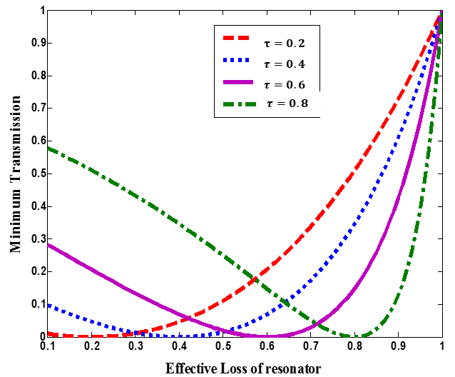 | Figure 6. Relationship between minimum transmission and effective loss of theresonator |
5. Bandwidth of the Transmission Characteristics
- The analysis is carried further to determine the 3-dB bandwidth of the power transmission characteristics
 . The maximum value of
  occurs when
  where
where  is an odd integer
 | (39) |
 and
and  satisfy the relation
 After simplification, one gets
 | (40a) |
 gives
gives | (40b) |
 , yields
  . Therefore, the full width-at-half maximum (FWHM) bandwidth of the transmission spectrum
  .The analysis of the transmission spectrum bandwidth
  is extended further to obtain a simplified expression related to practical designs. For high efficiency operation, the design of the ring modulator should satisfy the following two requirements(i) High-quality factor (Q) resonator to reduce the required applied voltage to switch the device from the ON state to OFF state (or vice versa).(ii) Operation under critical coupling to ensure maximum extinction ratio.The first requirement implies that
  deviates slightly from the resonance condition
  where
where  is a positive integer. Therefore,
  can be treated as a small angle relative to
  . Hence one can use the approximation
 to simplify eqn. (40b). The final result is
 | (41a) |
 | (41b) |
 | (41c) |
 | (42) |
 and can be considered as the resonance wavelength when
  . Here
  denote the lower and upper half-power wavelengths, respectively.Using eqn. (42) into eqn. (41) yields
 | (43) |
 with wavelength is not taken into account and it is assumed that
  for high Q-resonator. Otherwise,
  should be replaced by the group refractive index
 .It is worth to examine eqn. (43) under the condition of critical coupling where
  In this case
  | (44) |
 is given as
 | (45a) |
 | (45b) |
 (assuming strong coupling). The results are
 | (46a) |
 | (46b) |
 | (46c) |
 | (46d) |
 , both
  and
and  are proportional to the resonator circumference. This leaves the quality factor to be independent of L. Note further that
  approaches
  when
when  . This case corresponds to a lossless resonator where
  .
.6. Chirp Characteristics
- This section addresses the chirp (frequency modulation effect) when the device is used for analog intensity modulation. The phase characteristics of the output transfer function is governed by the following expression
 | (47) |
 is related to
  by
by | (48a) |
 with
with  is the speed of light in vacuum, the wavelength chirp is then computed as
 | (48b) |
 is a function of the angle
  which is a function of the applied voltage.From eqn. (32c), it is clear that
  is a function of
  and the coupling length
  is voltage dependent. Therefore, the frequency chirp can be calculated as
  | (49) |
 is the total applied voltage consisting of a bias voltage
  and the ac modulating signal
  . Note that although the bias voltage does not affect
  it plays a key role in determining the chirp through the factor
  .From eqn. (47) and after using the relation
  , one gets
 | (50) |
 | (51a) |
 | (51b) |
 | (51c) |
 | (51d) |
 can be computed from
 | (52a) |
 | (52b) |
 value.(ii) Positive DC voltage should be used to achieve low chirp intensity modulation.
7. Modulation Bandwidth
- Three factors affect the modulation bandwidth of the modulator under investigation (i) Modulator RC time constant(ii) Modulator photon lifetime(iii) Bandwidth limitation of the derive circuit.Parallel-plate capacitance model can be used to estimate the modulator capacitance that seen between the two contacts
 | (53) |
 . Here
  represents the permittivity of the vacuum. Further
  and
and  represent slot height and width, respectively. The bandwidth due to RC time constant is
  where
where  is the loading resistance and sets to
  in the simulation. Note that
  is directly proportional to slot width and inversely proportional to both slot height and phase shifter length.The modulation bandwidth due to photon lifetime
  is related to photon life time
  by [44]
 | (54) |
 | (55) |
 (per unit time) which is equivalent to the rate
  per cycle, where T is the period of the optical wave. Therefore
 | (56a) |
 | (56b) |
 | (57a) |
 | (57b) |
 .
.8. Electrical Power Consumption
- The electrical power dissipated during switching the modulator from one state (applied voltage = 0) to another state (applied voltage=
 ) can be considered mainly due to charging (or discharging) the modulator capacitor. To calculate this dissipated power, the modulator under investigation is modeled simply as a series RC network driven by a voltage source
  through a switch S whose operating state (i.e., ON or OFF state) is controlled by the binary modulating bits (see Fig. 7).
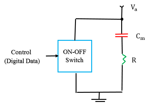 | Figure 7. Simplified model to calculate the electrical power consumption during the switching modulator state |
 is given by
 | (58a) |
 | (58b) |
 , where
  is the bit rate, can be calculated as
 | (59a) |
 and therefore
 | (59b) |
 is independent of the resistance R. Few remarks related to the switching dissipated power
  can be noted here (i) The power consumption associated with discharging the modulator capacitance (i.e., the switch is off in Fig. 7) is also governed by eqn. (59).(ii) In driving the modulator with real binary digital signal, the number of charge discharge cycles depends on the pattern of bits. In average, there is one complete charge/discharge cycle every four bits under the assumptions of equal numbers of "Ones" and "Zeros" are transmitted [46]. This can be understood by observing two successive bits which fall into four equally likely sequences (11, 00, 01 and 10). In the first two sequence, there is no change of state, so no energy is dissipated in charging the capacitance [46]. Therefore, the actual average dissipated power is
  . In other words, the average dissipated energy per bit is given by
 | (60) |
 . Note that the modulator capacitance depends only on the slot structure parameter (i.e., polymer refractive index
  and slot dimensions
  ).(iv) If the stray capacitance due to the connection with driving circuit is included in the calculation, then the effective modulator capacitance increases and this will increase the dissipated power.
9. Extinction Ratio and Insertion Loss
- Assume the modulator is excited by an optical signal having a wavelength equal to modulator resonance wavelength
 associated with zero applied voltage
  . (See Fig. 8a). Figure 8b shows the transmission characteristics as a function of wavelength for two values of applied voltages. The applied voltage
  shifts the resonance frequency. Positive values of
  increases the polymer refractive index and hence introduce red shift to the resonance frequency.In decibel scale, the insertion loss (IL) and extinction ratio (ER) are defined as
 | (61) |
 | (62) |
 Hence
Hence | (63) |
 is the insertion loss when
  .Note that the summation of insertion loss and extinction ratio is independent of applied voltage and it is equal to
  | (64) |
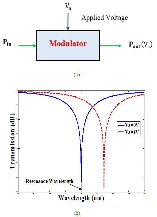 | Figure 8. (a) Basic modulator model. (b) Modulator transmission characteristics versus wavelength |
10. Conclusions
- A design methodology has been explained for an optical ring modulator incorporating silicon-polymer-metal hybrid plasmonic phase shifter. Analytical expressions have been derived to characterize the transmission characteristics and performance parameters of this modulator. The results can be used as a guide line to design compact modulators for optical communication wavelengths.
ACKNOWLEDGMENTS
- The work is a part of a PhD research program in the Institute of Laser for Postgraduate Studies, University of Baghdad, Iraq. One of the authors, Mrs. Al-mfrji, wishes to thank the College of Engineering at Al-Nahrain University, Baghdad, Iraq, for offering her the PhD scholarship.
 Abstract
 Reference
 Full-Text PDF
 Full-text HTML