Shayan Saeidi, Hassan Kaatuzian
Photonics Research Laboratory (P.R.L.), Electrical Engineering Dept., Amirkabir University of Technology, Tehran, Iran
Correspondence to: Shayan Saeidi, Photonics Research Laboratory (P.R.L.), Electrical Engineering Dept., Amirkabir University of Technology, Tehran, Iran.
| Email: |  |
Copyright © 2015 Scientific & Academic Publishing. All Rights Reserved.
Abstract
In this paper, improving internal quantum efficiency of a tensile-strained n-type Germanium in Si/SiGe/Si heterojunction laser has been analysed in theory. We discuss substituting Ge with an Alloy Si0.05Ge0.95, as active laser medium, sandwiched between n-Si(100) and p-Si(100). This new structure lowers mismatching and will be CMOS compatible for Integrated Photonic circuits. The results of our analysis, compared with former experimental reports in Si/Ge/Si semiconductor laser, demonstrate considerable improvement of efficiency and reliability. The internal quantum efficiency as high as 50% can be obtained in the proposed device which is a noteworthy achievement for an indirect bandgap material. We also study if this substitution has an impact on optical gain; Therefore, we theoretically discuss the effect of substituting tensile-strained germanium with tensile strained silicon-germanium alloy on the direct-gap optical gain, and the results are compared with each other. It can be seen that the optical gain of the proposed device has been slightly improved. The optical gain of proposed device in both strained and unstrained cases is also analysed and compared.
Keywords:
Silicon-Germanium, Internal Quantum Efficiency, Optical Gain, Silicon Photonics
Cite this paper: Shayan Saeidi, Hassan Kaatuzian, Theoretical Estimation to Improve Optical Characteristics of Germanium Lasers for Integrated Silicon Photonics Application, International Journal of Optics and Applications, Vol. 5 No. 3, 2015, pp. 65-70. doi: 10.5923/j.optics.20150503.03.
1. Introduction
Over the past decades, there has been a significant improvement in information technology mostly caused by decreasing the size of transistors. This attitude was predicted by Moore’s Law, which claims that number of integrated circuits doubles almost every 18 months. Such a trend leads to other problems as heat concern, losses of resistance, and so on. Therefore, these problems will not allow Moore’s Law to scale. As technology makes smaller, communication between different parts of chips will be limited. Silicon photonics has been introduced as a promising solution of communication between different parts of chips. Semiconductor lasers play important roles for Silicon based photonic technology and among semiconductors, Ge is suggested as the only material capable of conforming to the CMOS standards and also be a light emitter for photonic integration [1]. However, progresses in optical communications demand for low cost high speed technology and thus, SiGe based devices are promising solutions for filling these gaps [2]. Fabrication of Ge laser has already been reported for experimental analysis, in which the Ge waveguides are grown epitaxially on Si using ultrahigh vacuum chemical vapour surrounding by SiO2 mask layer [3]. In this study, we suggest using a Si substrate at the above surface of device and analyse it vertically in order to demonstrate a Si/SiGe/Si p-n-n heterojunction, as shown in Figure 1.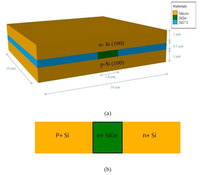 | Figure 1. (a) Cross sectional view of SiGe waveguide. (b) A schematic that shows the vertically view of structure with the p-type and n-type Si substrates doping of 1×1019 cm-3 and SiGe alloy with n-type doping of 1×1020cm-3 |
A similar p-n-n heterojunction was reported earlier [4]. In this study, we use specialized software semiconductor device simulator, to simulate this new proposed device. In simulation, the heterojunction is composed of two Si layer along each 1 μm with n-type and p-type doping of 1×1019 cm-3 and a 0.5 μm of SiGe with doping of 1×1020 cm-3 with composition of 95% Ge and 5% of Si. This composition leads to a better compatibility and lower mismatching with substrates around. We also investigate if this composition makes an improvement in internal quantum efficiency. Analytical and one-dimensional simulations are performed to study the effect of new proposed device on internal quantum efficiency.Another important characteristic of a semiconductor laser is its optical gain. We use reported relations and equations in order to calculate optical gain of both the proposed device, which silicon-germanium alloy is used as its active medium, and the former device in which germanium is defined as active medium. The peak gain for both structures, have almost the same result, but there is a difference in the wavelengths each device covers. We will study devices from this point of view.This paper is organized as follows. In section 2, first we’ll introduce physical structure for our proposed Germanium laser, which will be followed by reviewing theoretical equations and relations in order to calculate quantum efficiency. In section 3 we’ll illustrate the results of simulation and improvements of internal quantum efficiency obtained from substituting germanium with silicon-germanium in Si/Ge/Si p-n-n heterojunctions. Our work on calculating optical gain for both tensile-strained silicon-germanium alloy and germanium is presented in section 4. Eventually, the conclusion will be presented in section 5.
2. Quantum-Efficiency of Si/SiGe/Si
2.1. Structure of Device
The structure of device is shown in Figure. 1(a). The height of SiGe waveguide is 0.5 μm and the width is 1.6 μm [3]. The height of each Si substrate is 1 μm and the width and length dimensions are considered 10 μm. However simulation has been done in one-dimension. The vertical view of this structure is shown in Figure. 1 (b) (not all of the parts are shown).
2.2. Internal Quantum Efficiency
In order to calculate internal quantum efficiency (IQE), we have to consider radiative and nonradiative recombination rates. The recombination processes are given by [5]: | (1) |
In which A is the impurity recombination coefficient, B is the bimolecular coefficient, C is the Auger coefficient and N is also considered as carrier concentration. The bimolecular recombination rate is radiative while the rest is nonradiative. The A, B and C coefficients used in this calculation are 10-7 s-1, 10-14 cm3 s-1 and 10-31 cm6 s-1 respectively which were reported earlier in [5] and [6]. Since calculations are done in room temperature, carrier concentration can be estimated by Nd [7] and by considering high doping level and applied bias voltage Va, carrier density can be expressed as shown in (2), where K represents Boltzmann constant, T represents lattice temperature and q represents electron charge. | (2) |
The internal quantum efficiency of this heterojunction has been calculated from ratio of the bimolecular recombination rate in the active region to the total recombination rate, in other words, IQE is formed by: | (3) |
The results are in the scale of 10-3 which are comparable with simulation results (will be discussed in this paper). However, with increasing applied voltage, the nonradiative recombination rate which includes mostly Auger recombination, become significant at high carrier densities which leads to a decrease in quantum efficiency [4].For the verification of our software simulation, first of all, we tried to simulate the behaviours of a prefabricated p-n-n Si/Ge/Si hetero-junction laser device. The simulation results have had good agreements with experimental measurements reported before in [4]. Then we’ve tried to analyse and simulate the behaviour of our new proposed p-n-n Si/SiGe/Si laser device in comparison with previous one.
3. Simulation and Discussion on IQE
The simulation involves results from semiconductor device simulator SimWindows and general properties of Ge which were gathered from different resources ([8], [9]). In this simulation, all the lengths and doping levels are assumed as discussed in section 1. The Schockley-Read-Hall (SRH) lifetime needed for simulating is calculated by (4) in which the recombination time is modelled as a function of trap density NT, the trap-capture cross-sections for carriers σT, and thermal carriers’ velocities ν. The distance with surface is shown via y and surface recombination velocities are represented by sn,p [10]. However, surface recombination velocities are not considered in simulation. | (4) |
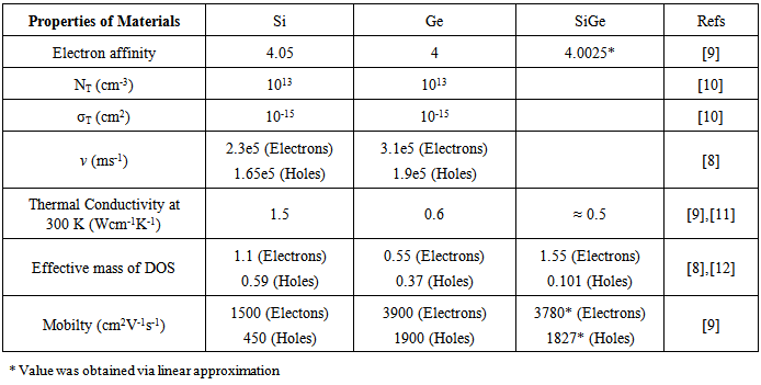
Some of the important parameters required for simulation can be seen in Table.1. In the proposed device, general properties and values of SiGe were calculated either using a linear approximation or derived through observations of a diagram. Equation (5) is the linear approximation which includes the value of Silicon VSi, the value of Germanium VGe and the percentage of composition x (in this case 0.95) [9].  | (5) |
Table 1. Properties of Materials
 |
| |
|
The values for energy gap were determined from following expressions [8]: | (6) |
 | (7) |
The recombination coefficients used in simulation are the same as ones discussed in section 2. The simulated internal quantum efficiency versus forward bias for both p-n-n Si/Ge/Si heterojunction and p-n-n Si/SiGe/Si is shown in Figure.2. It can be observed that internal quantum efficiency improves about two orders of magnitude with substituting Ge with an alloy SiGe in Si/Ge/Si heterojunction, thus, the internal quantum efficiency as high as 50% can be obtained in the proposed device which is a noteworthy achievement for an indirect bandgap material. It is encouraging for efficiency of tensile-strained n+ Ge to reach similar quantum efficiencies on Si.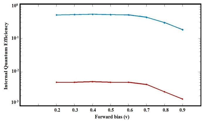 | Figure 2. Simulated internal quantum efficiency versus forward bias for p-n-n Si/Ge/Si heterojunction (red line) and p-n-n Si/SiGe/Si heterojunction (blue line) |
The amount of internal quantum efficiency increases with growth of applied voltage, however it begins to diminish above the forward bias of almost 0.6 V for both types of heterojunctions because nonradiative recombination processes become significant at high injected carrier densities and begins to control carrier density [4].
4. Optical Gain in Silicon-Germanium
The direct gap optical gain of Ge tensile strained has been reported earlier [4], [13]. The gain coefficient of the direct band transition is related to absorption coefficient of the direct band transition by:  | (8) |
The expression, (fc – fv), shows the population inversion factor which is calculated based on Fermi- Dirac distribution. For tensile-strained Ge, absorption coefficient of the direct band transition can be expressed as following [14]: | (9) |
Which  and
and  are direct bandgaps related to light hole and heavy hole bands to direct valley, respectively, and constants 0.318 and 0.682 are related to contribution of light and heavy hole bands to the total absorption relying on their reduced effective mass. Coordinating to experimentally measured absorption results A= 2.01 × 10⁴ eV1/2cm-1 for tensile strained germanium. However, since we are considering Si0.05Ge0.95 as the active medium of device in which 95 percent is based on germanium, these constants seem fair to be used in this study. The dependence of direct bandgaps of SiGe related to tensile strain has been derived from deformation potential theory.According to earlier reports [15], bandgap of silicon-germanium as a function of strain and germanium fraction was calculated using deformation potential theory, in which the bandgap of alloys with germanium fraction less than 0.85, reduces strongly with strain both in tension and compression modes, however for alloys with germanium fraction greater than 0.85 the bandgap decreases only in tensile-strained case. Since we are studying germanium fraction of 0.95, the band structure of 0.25% tensile strain silicon-germanium, represents that direct bandgap related to light hole to direct valley reduces to 0.7 eV.The optical gain of 0.25% tensile strained Ge and SiGe had been calculated and compared in Figure. 3. These calculations, as discussed, are based on direct band to band transition model. The shoulders of optical gain for both materials indicates the optical transition between light and heavy hole bands and the direct valley. It can be seen that the optical gain of the proposed device has been slightly improved. Although this improvement is not impressive, but it has broadened the gain spectrum and it has shifted the optical gain peak to lower photon energies at about 0.72 eV which is at 1700 nm. Therefore, the optical gain spectrum covers longer wavelengths. It’s good to notice that the wavelength of 1550 nm which is calculated for tensile-strained germanium (peak optical gain at 0.8 eV) is more desirable for communication applications. This spectrum provides a peak optical gain of 1400 cm-1 which is similar to a direct bandgap material.
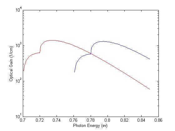 | Figure 3. Optical gain spectra of germanium (blue line) and silicon-germanium alloy (red line) |
The effect of tensile strain on optical gain of silicon-germanium alloy has been approximately shown in Figure. 4 and the strained and unstrained Si0.05Ge0.95 are compared. As it can be seen the shoulder observed in tension case has been removed since light and heavy hole bands have same energy and both have the same momentum as direct valley. The optical gain in strained case has been improved, however this enhancement is not over a magnitude because the strain level, 0.25%, is low compared to the strain level of 1.8% which leads to a direct bandgap germanium. The bandgap of silicon-germanium alloy as a function of strain (0.25%) and germanium fraction (95%) has been obtained from [15], calculated using deformation potential theory.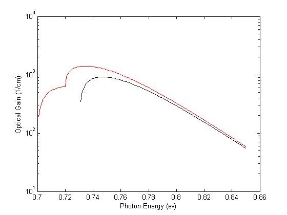 | Figure 4. Optical gain spectra of silicon-germanium alloy in strained case (red line) and unstrained case (blue line) |
5. Conclusions
In this paper, we proposed a device in which SiGe replaces Ge in Si/Ge/Si heterojunction. The active medium of this device is more compatible with surrounded Silicon layers which lead to less mismatching. The internal quantum efficiency of n-type doped Ge heterojunction is calculated and the results agree with the simulated one. Therefore, we study the properties of SiGe heterojunction, internal quantum efficiency for both type of (p+Si/n+Ge/n+Si) and (p+Si/n+SiGe/n+Si) was simulated and compared. It is shown that internal quantum efficiency improves for about two orders of magnitude compared to Ge heterojunction. In the following, it could be seen that the results were promising and internal quantum efficiency as high as 50% can be obtained.The effect of tensile strain on optical gain in silicon-germanium alloy is approximately calculated. It could be clearly seen that optical gain will slightly improve and it covers wider range of wavelengths in case of using SiGe alloy instead of germanium. However, the calculated wavelength of optical gain’s peak (1700nm) is not very suitable for fiber communication applications, but the use of silicon-germanium is recommended over germanium because of its more compatibility with silicon based technology.
References
| [1] | R. E. Camacho-Aguilera, “Ge-on-Si LASER for Silicon Photonics,” Massachussets Institute of Technology, 2013. |
| [2] | H. Davoodi, H. Kaatuzian, “Base Composition Effects Study On NBR Current and Current Gain in SiGe HBT,” Int. J. Mod. Phys. B 27, 1350097, 2013. |
| [3] | J. Liu, X. Sun,R. Camacho-Aguilera, L. C. Kimerling, and J. Michel, “Ge-on-Si laser operating at room temperature,” Opt.Lett.35, 679-681, 2010. |
| [4] | X. Sun, J. Liu, L. C. Kimerling, and J. Michel, “Toward a Germanium Laser for Integrated Silicon Photonics,” Selected Topic in Quantum Electronics, IEEE Journal of 16, 124-131, 2010. |
| [5] | S. Marchetti, M. Martinelli, R. Simili, M. Giorgi, and M. Fantoni, “measurement of ge electrical parameters by analysing its optical dynamics,” Phys. Scr., vol 64, pp 509-511, 2001. |
| [6] | Smirl A. L., Moss S. C. and Ryan Lindle J., “Picosecond dynamics of high-density laser-induced transient plasma gratings in germainum”, Phys. Rev. B 25, 2645, 1982. |
| [7] | H. Kaatuzian, “Photonics,” 3rd ed., vol 1, AKU Press, 2012. |
| [8] | “Semiconductors on NSM,”http://www.ioffe.ru/SVA/NSM/Semicond/. |
| [9] | Virginia Semiconductor, “The General Properties of Si, Ge, SiGe, SiO2 and Si3N4,” 2002. |
| [10] | V. Palankovski, R. Quay, “Analysis and Simulation of Heterostructure Devices,” Springer:Wien, 2004. |
| [11] | Stohr, H., W. Klemm, Z. Anorg. Allgem. Chem. 241, 1954, 305. |
| [12] | R. F. Pierret, Modular Series on Solid State Devices, vol 1, Addison-Wesley, 1983. |
| [13] | J. Liu, X. Sun, D. Pan, X. Wang, L. C. Kimerling, T. L. Koch, J. Michel, “Tensile-Strained, n-type Ge as a gain medium for monolithic laser integration on Si,” Opt. Exp., vol. 15, pp. 11272-11277, 2007. |
| [14] | J. Liu, L. C. Kimerling, J. Michel, “Monolithic Ge-on-Si lasers for large-scale electronic-photonic integration,” Semicond. Sci. Technol., vol. 27, 2012. |
| [15] | Laura Marie Giovane, “Strain-Balanced silicon-germanium materials for near IR photodetection in silicon based optical interconnects,” Massachussets Institute of Technology, 1993. |
 Abstract
 Reference
 Full-Text PDF
 Full-text HTML