-
Paper Information
- Paper Submission
-
Journal Information
- About This Journal
- Editorial Board
- Current Issue
- Archive
- Author Guidelines
- Contact Us
International Journal of Optics and Applications
p-ISSN: 2168-5053 e-ISSN: 2168-5061
2014; 4(3): 92-100
doi:10.5923/j.optics.20140403.04
Analytical Framework to Investigate the Performance of WDM Cascade Demultiplexer
 Abstract
 Reference
 Full-Text PDF
 Full-text HTML
1Department of Laser and Optoelectronics Engineering, Alnahrain University, Baghdad Iraq
2Department of Computer Engineering, Alnahrain University, Baghdad, Iraq
Correspondence to: R. S. Fyath, Department of Computer Engineering, Alnahrain University, Baghdad, Iraq.
| Email: |  |
Copyright © 2014 Scientific & Academic Publishing. All Rights Reserved.
The aim of this paper is to present a framework to analysis the performance of wavelength-division demultiplexers incorporating cascaded stages. Each stage is used as a single-channel drop filter. The analysis is based on the coupled-mode theory (CMT) and takes into account the interaction between successive stages. The CMT is first applied to characterise a single-channel demultiplexer and the results are used to drive expressions for its scattering parameters. Then the analysis is extended to a multi-channel demultiplexer using matrix formulation in order to calculate the scattering parameters related to various ports. Simulation results are presented for two 3-channel demultiplexers, namely (1550, 1300, 850 nm) and (1650, 1550, 1450 nm) demultiplexers. The results reveal that the interaction between successive stages should be taken into account to extract the demultiplexer performance accurately.
Keywords: WDM Demultiplexer, Cascade Demultiplexer, Coupled-Mode Theory
Cite this paper: Rasha H. Mahdi, R. S. Fyath, Analytical Framework to Investigate the Performance of WDM Cascade Demultiplexer, International Journal of Optics and Applications, Vol. 4 No. 3, 2014, pp. 92-100. doi: 10.5923/j.optics.20140403.04.
Article Outline
1. Introduction
- Wavelength-division multiplexing (WDM) is one of the commonly used technologies to increase the capacity of optical communication systems [1-3]. In WDM system, multiple wavelength carriers, each modulated by relatively low bit rate, are grouped (multiplexed) at the transmitter side before launching into the fiber link. At the receiver side, the WDM signal is separated (demultiplexed) to individual wavelengths. Generally, the capacity of WDM system is scaled by the number of used channels (wavelengths). Optical demultiplexers are key components in WDM systems and should be designed carefully to extract the single channel at the base rate where electronics can be used. In the past few years, there has been a tremendous interest in the design of WDM demultiplexers using plasmonic technology [4, 5], photonic crystal technology [6, 7], and silicon photonic platform [8, 9].One of the simplest methods to design multiple-channel demultiplexers is based on cascade configuration [10-12]. Here the demultiplexer consists of multiple units connected in series; each one is tuned to drop one wavelength (see Fig. 1). Each unit behaves as a narrow bnndpass filter and can be implemented using different techniques.
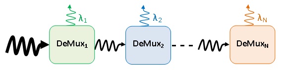 | Figure 1. Concept of a cascade demultiplexer. DeMuxi represents the ith unit used to drop the ith wavelength λi |
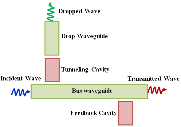 | Figure 2. Schematic diagram of a single-channel demultiplexer consisting of a drop nanocavity coupled with a feedback nanocavity |
2. Background
- This section presents CMT formulation for an optical configuration containing a cavity coupled laterally to a waveguide. The analysis stands heavily on the formulation reported in [15] which has been used widely by other workers [13, 14, 16-20].
2.1. Analysis of Channel Drop Filter Cavity
- Figure 3 shows the basic structure of a cavity which is side coupled to a bus waveguide and axially coupled to a drop waveguide. The cavity is used for a resonant tunnelling-based drop operation. The structure is treated as a three-port system with a reference plane passing through the centre of the cavity. It is assumed that the cavity, bus waveguide, and drop waveguide support single mode in the frequency range of interest with negligible nonlinear optics effect. The cavity possesses mirror reflection symmetry with respect to the reference plane. The amplitude of the incoming waves are denoted by
 and
and  . The amplitudes of the outgoing waves are denoted by
  and
and  .
.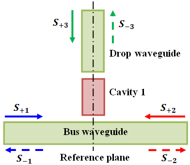 | Figure 3. Channel drop filter with cavity 1 used for a resonant tunnelling-based channel drop operation |
 | (1) |
 = Cavity field amplitude.
 = Resonance frequency of the cavity.
 = Quality factor due to intrinsic loss.
 = Quality factor of the cavity which is connected with rate of decay into the bus waveguide.
 = Quality factor of the cavity which is related to the rate of decay into the drop waveguide.
 = Phase of the coupling coefficient between the cavity and the bus waveguide.
 = Phase of the coupling coefficient between the cavity and the drop waveguide.The incoming and outgoing waves can be described as
 | (2a) |
 | (2b) |
 | (2c) |
 . Assume that
  has a
has a  time dependence. Due to the linearity of the system under observation, each wave can be expressed as
  , where
  is the complex amplitude.Using
  and
and 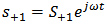 in Eqn. (1), with
 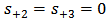 , yields
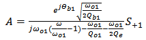 | (3a) |
 | (3b) |
 , yields the following expressions describing the reflection
  at the input port, the transmission
  through the bus, and the transmission
  through the drop port
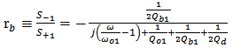 | (4a) |
 | (4b) |
 | (4c) |
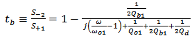
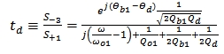
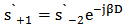
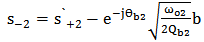
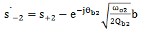
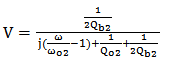
2.2. Analysis of Wavelength-Selective Reflection Cavity
- Figure 4 shows the basic structure of a feedback cavity side coupled to a bus waveguide. It is assumed that both the cavity and bus waveguide support single mode in the frequency range of interest with negligible nonlinear optics effect. The cavity possesses mirror reflection symmetry with respect to the reference plane. The amplitudes of the incoming waves are denoted by
 and
and  . The amplitudes of outgoing waves are denoted by
  and
and  .
.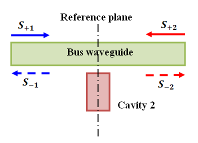 | Figure 4. Basic structure of a waveguide side-coupled to cavity 2 which is used to realize the wavelength-selective reflection function |
 | (5) |
 = Cavity field amplitude.
 = Resonance frequency of the cavity.
 = Quality factor due to intrinsic loss.
 = Quality factor due to the rate of decay into the bus waveguide.
 = Phase of the coupling coefficient between the cavity and the bus waveguide.The outgoing waves are given by
 | (6a) |
 | (6b) |
 time dependence. Using
  and assuming the input signal is applied at port 1 (i.e.,
  ) then Eqn. (5) gives
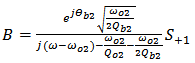 | (7) |
 | (8a) |
 | (8b) |
 ), then Eqns. (8a) and (8b) reduce to Eqns. (9a) and (9b), respectively
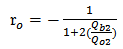 | (9a) |
 | (9b) |
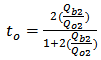
 , then
  and
and  tend to 1 and 0, respectively.The full-width at half-maximum (FWHM) of the reflection spectrum can be obtained after finding the half power cut-off frequencies
 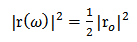 | (10) |
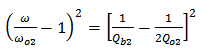
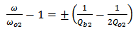 | (11) |
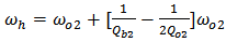 | (12a) |
 | (12b) |

 | (13a) |
 | (13b) |
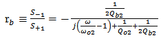
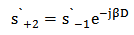
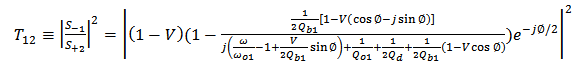
3. Analysis of Single-Channel Demultiplexer
- The single-channel demultiplexer can be represented as two cavities coupled to a waveguide with one drop port. As seen in Figure 5. The cavities 1 and 2 are used to realize resonant tunnelling-based channel drop filterer and wavelength-selective reflection feedback, respectively. The structure can be considered as a three-port network where ports 1, 2, and 3 represent, respectively, the input port, the output port, and the drop port.
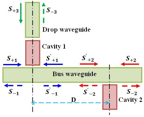 | Figure 5. Schematic diagram of demultiplexer filter based on the resonant tunneling effect of the cavity (i.e., Cavity 1) near a bus waveguide with a side-coupled reflection cavity (i.e., Cavity 2) |
 | (14a) |
 | (14b) |
 = Resonance frequency of cavity 1.
 = Resonance frequency of cavity 2.
 = Quality factor due to intrinsic loss of cavity 1.
 = Quality factor due to intrinsic loss of cavity 2.
 = Quality factor of cavity 1 that is connected with rate of decay into the bus waveguide.
 = Quality factor of cavity 2 that is connected with rate of decay into the bus waveguide.
 = Quality factor of cavity 1 that is related to the rate of decay into the drop waveguide.
 = Phase of the coupling coefficient between cavity 1 and the bus waveguide.
 = Phase of the coupling coefficient between cavity 2 and the bus waveguide.
 = Phase of the coupling coefficient between the cavity 1 and the drop waveguide.The incoming and outgoing waves can be described as
 | (15a) |
 | (15b) |
 | (15c) |
 | (15d) |
 | (15e) |
 | (15f) |
 | (15g) |
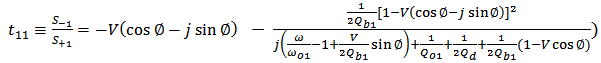
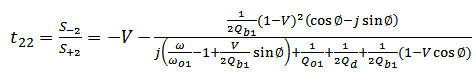
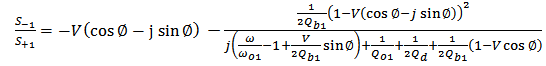
 ), then the optical scattering coefficient can be expressed as (see Appendix for details)
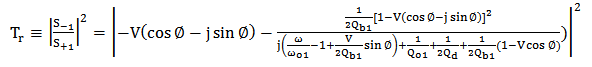 | (16a) |
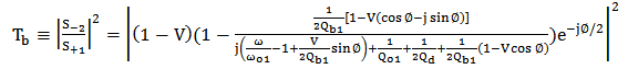 | (16b) |
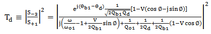 | (16c) |
 | (17a) |
 | (17b) |
 = Phase between the two reference planes.
 = Propagation constant of the bus waveguide.
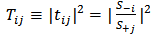
 = Distance between the two reference planes.It is worthing to introduce the amplitude and power scattering parameters from port
  to port
 | (18a) |
 | (18b) |
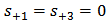
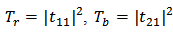 , and
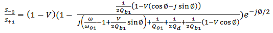
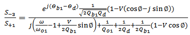
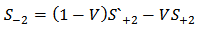
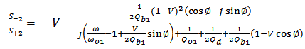
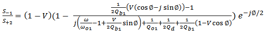
, and  .The analysis is carried further to investigate the demultiplexer characteristics when the incoming optical signal is applied at port 2. This is useful to characterise the behaviour of a multi-channel demultiplexer implemented by cascading multi single-channel units. Inserting
 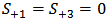 in Eqns. (14) and (15) yields (see Appendix for more details)
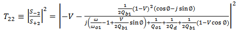 | (19a) |
 | (19b) |
 | (19c) |
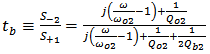
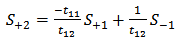
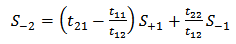
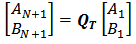
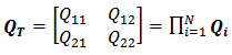
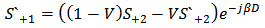
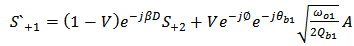
4. Analysis of Multi-Channel Demultiplexer
- The aim of this section is to compute the scattering parameters of a multi-channel demultiplexer constructed by cascading single-channel demultiplexers (see Fig. 6(a)). In this figure, the forward and backward fields are presented by
 (solid lines) and
  (dashed lines), respectively. The
  stage of this configuration corresponds to the ith channel demultiplexer
  .
.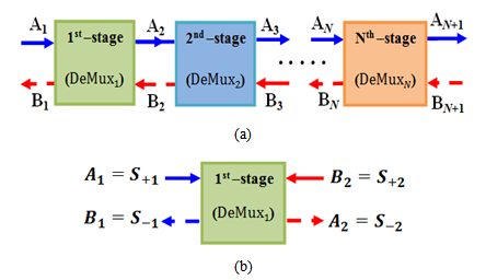 | Figure 6. (a) Block diagram of an N-channel cascade demultiplexer showing the forward fields (A) and backward fields (B). The drop ports are not shown for purpose of clarity. (b) The first channel demultiplexer |
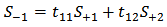
 . Here
  and
and  . This stage can be described using the concept of scattering matrix
 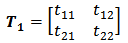 | (20a) |
 | (20b) |
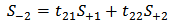 | (20c) |
 yields
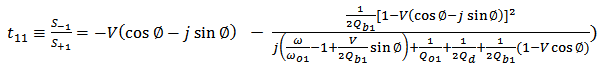 | (21a) |
 | (21b) |
 is set to zero
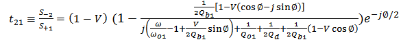 | (21c) |
 | (21d) |
 | (22a) |
 | (22b) |
 | (23a) |
 | (23b) |
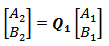
 relates the fields at port 2 to those at port 1. The elements of the matrix
  are
are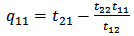 | (24a) |
 | (24b) |
 | (24c) |
 | (24d) |
 demultiplexer
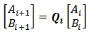 | (25) |
 | (26a) |
 | (26b) |
 ), then the reflection and transmission coefficients can be expressed as
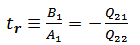 | (27a) |
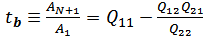 | (27b) |
 from Eqn. (27b) and
  ). Then one can go in opposite direction from port (N+1) to port 1 to determine the field components
  and
and  for each demultiplexer unit. For example, for the Nth channel demultiplexer
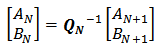 | (28a) |
 channel demultiplexer
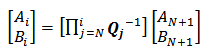 | (28b) |
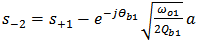
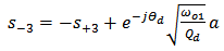
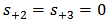
 for the case under observation.The above analysis can be extended further to calculate the signal waves at the drop ports. Let the drop port of the ith demultiplexer is denoted by
  (see Fig. 7). Note that
  and
and 
 | Figure 7. Basic description of the single-channel demultiplexer including the drop port |
 (i.e.,
  ), then
 | (29a) |
 | (29b) |
 | (29c) |
 | (29d) |
5. Simulation Results
- Simulation results are presented for two three-channel demultiplexers, (1550, 1300, 850 nm) and (1650, 1550, 1450 nm). The parameters values used in the simulation are
 ,
,  ,
,  ,
,  , and
, and  . Further,
  .The spectral characteristics of the two demultiplexers are displayed in Figs. 8 and 9, respectively. Each figure contains three parts with part “a” displays the drop efficiency at each of the three ports. Parts “b” and “c” show, respectively, the power transmission coefficient at the demultiplexer output port and the power reflection coefficient at the demultiplexer input port. Comparing the result in Fig. 8(a) and Fig. 9(a) reveals the effect of the channel spacing on the drop efficiency.
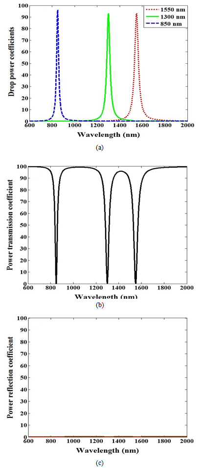 | Figure 8. Power spectra associated with the (1550, 1300, 850 nm) demultiplexer. (a) Drop efficiency at each of the three ports. (b) Power transmission coefficient at the output port. (c) Power reflection coefficient at the input port |
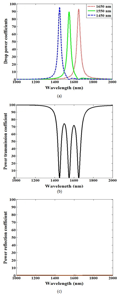 | Figure 9. Power spectra associated with the (1650, 1550, 1450 nm) demultiplexer. (a) Drop efficiency at each of the three ports. (b) Power transmission coefficient at the output port. (c) Power reflection coefficient at the input port |
6. Conclusions
- This paper has presented a methodology for the analysis of a multi-channel WDM demultiplexer incorporating cascaded stages. The scattering parameters of each stage have been derived using CMT and the results have been used to characterise the performance of the multi-channel demultiplexer using signal flow transformation. The analysis can be used as a guideline to address the effect of interference between adjacent channels in WDM demultiplexers.
Appendix
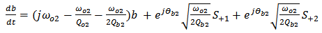
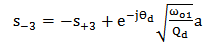
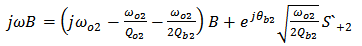
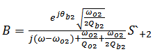
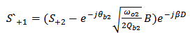
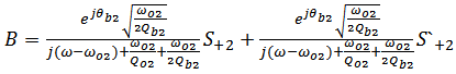
- Derivation of Transmission Coefficients of the Single-Cannel DemultiplexerThe single-channel demultiplexer under investigation consists of two cavities laterally coupled to a bus waveguide. The demultiplexer is treated as a three-port network as illustrated in section 3 and its characteristics is governed by Eqns. (14) and (15). The aim of this appendix is to derive the transmission coefficient of the demultiplexer when the signal is incident only at port 1 (forward-incident signal) or port 2 (backward-incident signal).a. Forward-Incident SignalSet
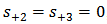 , and let
  , and b have a
  time dependence. then from Eqns. (14a) and (14b) one gets
 | (A1) |
 | (A2) |
 | (A3) |
 | (A4) |
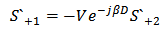 | (A5) |
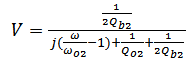 | (16a) |
 | (A6) |
 | (A7) |
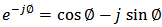 , one gets
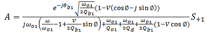 | (A8) |
 | (A9) |
 | (A10) |
 | (A11) |
 | (A12) |
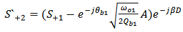
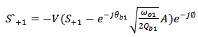
 , and let
  has a
has a  time dependence, then from Eqns. (14a) and (14b) one gets
 | (A13) |
 | (A14) |
 | (A15) |
 | (A16) |
 one gets
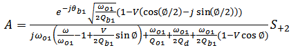 | (A17) |
 | (A18) |
 | (A19) |
 | (A20) |
 | (A21) |