-
Paper Information
- Next Paper
- Previous Paper
- Paper Submission
-
Journal Information
- About This Journal
- Editorial Board
- Current Issue
- Archive
- Author Guidelines
- Contact Us
International Journal of Optics and Applications
p-ISSN: 2168-5053 e-ISSN: 2168-5061
2014; 4(2): 46-53
doi:10.5923/j.optics.20140402.04
Simulation and Temperature Characteristics Improvement of 1.3μm AlGaInAs Multiple Quantum Well Laser
 Abstract
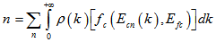
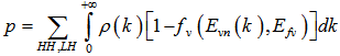
 Reference
 Full-Text PDF
 Full-text HTML
Vahid Bahrami Yekta, Hassan Kaatuzian
Photonics Research Laboratory (PRL), Electrical Engineering Department, Amirkabir University of Technology, Tehran, Iran
Correspondence to: Hassan Kaatuzian, Photonics Research Laboratory (PRL), Electrical Engineering Department, Amirkabir University of Technology, Tehran, Iran.
| Email: |  |
Copyright © 2014 Scientific & Academic Publishing. All Rights Reserved.
In this paper the effects of strain on the barriers of a 1.3 μm AlGaInAs-InP multiple quantum well laser are investigated by solving Kohn-Luttinger and effective mass equations. The results have shown that many enhancements can be made to the laser structure by introducing 0.2% compressive strain to the barriers. 20% improvement in mode gain-current density characteristic and 3% improvement in material gain spectra were obtained while the leakage and Auger currents reduced significantly. Energy levels in conduction and valence bands are calculated and used to simulate the material gain. The effects of temperature increase on the recombination and Auger current densities are also investigated.
Keywords: AlGaInAs-InP multiple quantum well laser, Uncooled laser, Strain in barrier, Kohn-Luttinger hamiltonian
Cite this paper: Vahid Bahrami Yekta, Hassan Kaatuzian, Simulation and Temperature Characteristics Improvement of 1.3μm AlGaInAs Multiple Quantum Well Laser, International Journal of Optics and Applications, Vol. 4 No. 2, 2014, pp. 46-53. doi: 10.5923/j.optics.20140402.04.
Article Outline
1. Introduction
- The performance of the semiconductor laser has been dramatically improved since its invention in 1962. Today it came to be indispensable for our life as optical components connecting home and the Internet as well as long-distance large-capacity trunk networks. Wavelengths used for optical communication are mainly 1.55 μm for long-distance transmission and 1.3 μm for short- and mid distance transmission due to the minimum loss and minimum dispersion in optical fiber. It is required that the band gap of the material composing semiconductor laser correspond to the oscillation wavelength of the laser and its lattice constant match to the lattice constant of the substrate to maintain high crystal quality. Typical compound semiconductors that meet these conditions are GaInAsP, AlGaInAs grown on the InP substrate and GaInNAs, (Ga)InAs dots structure grown on the GaAs substrate. Today, GaInAsP is widely used from view points of reliability of device and handling in its process. The lattice constant and the band gap of a compound semiconductor can be controlled by changing the composition of the compound. In the structure that two compound semiconductors with different band gaps pile up alternatively, electrons and holes are confined in the lower band gap layers. The thickness of the lower band gap layer approaches to electron mean free pass (several 10 nm), energy levels of electron and hole are quantized. This structure is called quantum well (QW) or multiple quantum well (MQW) when the structure consists of multiple layers. In the MQW structure, novel phenomenon which cannot be obtained in the bulk material appears. By applying MQW structure to the active region of the laser, the performances of the laser such as threshold current, temperature characteristics and modulation frequency were significantly improved and MQW became an essential technology for realizing high performance lasers.Uncooled laser that can operate at room temperature with a stable wavelength and output power is very desirable. Commercial GaInAsP laser needs to have huge cooling system which is caused mainly by poor confinement of electrons in the conduction band due to relatively small conduction band offset (∆Ec = 0.4∆Eg). The effective mass of electrons in conduction band is much less than the effective mass of holes in valence band so the laser efficiency increases more with making stronger barriers for electrons rather than holes at high temperatures. Large conduction band offset up to (∆Ec = 0.72∆Eg) is achieved with AlGaInAs barriers and wells [1].When a MQW system is pumped, the carriers travel in the barriers and drop in the quantum wells. The excess carriers separate the Fermi level into two quasi Fermi levels. The separation between two quasi Fermi levels depends on the pump strength. When the pump is strong enough to a separation equal to the material bandgap, the material becomes transparent for photon energies equal to the bandgap. Optical gain is achieved when the system is pumped beyond transparency condition. The differential gain is the rate that the gain increases with carrier density. It depends on how quickly the band edge carrier density can be increased. The band edge carrier density can be increased by symmetric band structure (mc = mv) and steep change in density of states. Both these conditions exist in strained quantum well. Two dimensional density of state has a perfect step like shape and the effective masses can be adjusted by the strain of the well.Strain in barriers enhances the effective mass of the injected carriers and the quantum wells are populated more efficiently as more carriers can get into the wells before recombination. This effect has been investigated and calculated in this paper. We used COMSOL Multiphysics software to solve Kohn-Luttinger Hamiltonian equations for finding valence band energy levels and single band effective mass equation to find conduction band energy levels. At first we simulated the structure that was fabricated and presented in [2], it is a MQW ridge wave guide AlGaInAs-InP laser with lattice match barriers, Then we investigated the same structure with 0.2% compressive strain and 0.2% tensile strain barriers. (see Figure 1)In section II we introduce the theoretical model for simulating the structure. In section III we describe and discuss the simulation results and improvements. We have a conclusion section at the end.
2. Theory
2.1. Energy Levels in Conduction and Valence Bands
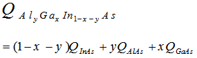
- Figure 1 shows the under study structure. It is a ridge wave guide laser diode. It has active layer with five quantum wells and four barriers between them. Two graded index layers and two spacer layers enwind the active layer.
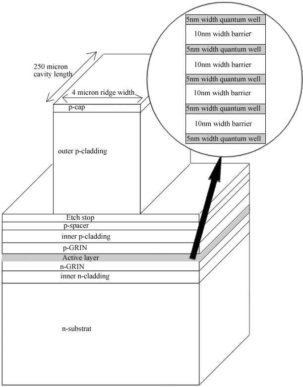 | Figure 1. The ridge wave guide laser structure under study |
|
 | (1) |
 : Envelope function;
 : Planck's constant divided by 2π;
 : Electron effective mass in conduction band;
 : Conduction band potential;
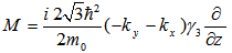
 : Electron energy level in conduction band;The strain can be compressive or tensile. According to Figure 2 we can see the effect of strain on the conduction and valence band structure in a strained quantum well.
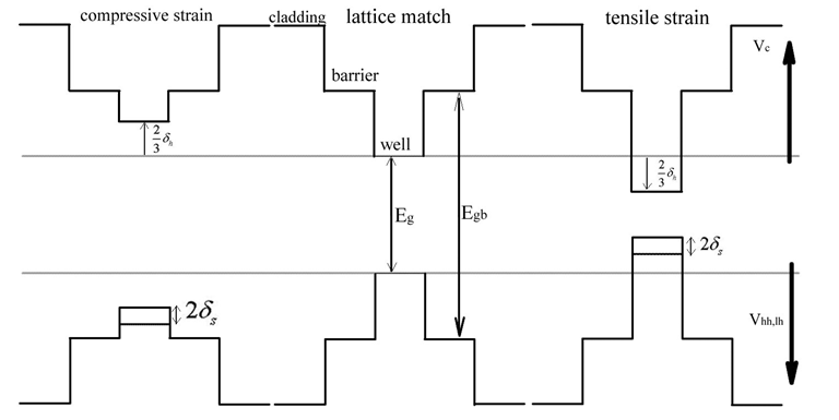 | Figure 2. Effect of strain on conduction and valence bands in MQW |
 | (2) |
 | (3) |
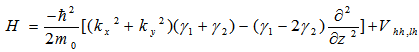
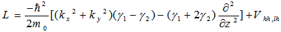
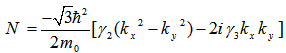
 : Elastic stiffness constants;The valence band structure in quantum well is not parabolic, so multi band effective mass theory is used [4] we solve the resulting coupled differential equations known as Kohn-Luttinger Hamiltonian equations for finding heavy and light holes energy levels and Envelope functions [3]
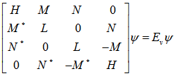 | (4) |
 | (5) |
 | (6) |
 | (7) |
 | (8) |
 : luttinger parameters;
 : Components of the transverse wave vector;
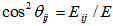
 : Potential of heavy and light holes in the valence band;In Figure 2 δs is the shear potential and defined as follows [3]
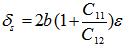 | (9) |
 | (10) |
 | (11) |
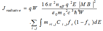
2.2. Optical Gain and Current Models
- The optical gain transition depends on the polarization and as a function of photon energy can be written as [13]
 | (12) |
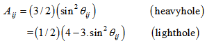
 : Bulk momentum transition matrix element;i,j : quantum numbers in conduction and valence band;
 : Spatial overlap factor;
  : Angular anisotropy factor;
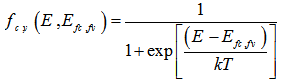
 : Electron Fermi functions;
 is the Lorentzian line shape function that convolved with gain spectra to determine the effects of intra band transitions [14]. Each individual transition contributing to the gain continuum is itself broadened by scattering.
 | (13) |
 is the intra band relaxation time that we choose it 0.1ps according to [2].The carrier effective mass in the ith sub band can be calculated from [5]
 | (14) |
 confinement factor of the carrier Envelope function in the Quantum well for nth sub band;mw: carrier effective mass in the well that calculate by quaternary formula;mb: carrier effective mass in the barriers that calculate by quaternary formula;So the reduced effective mass between ith conduction sub band and jth valence sub band is obtained [5]
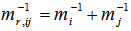 | (15) |
 | (16) |
 | (17) |
 | (18) |
 | (19) |
 | (20) |
 | (21) |
 | (22) |
 | (23) |
 | (24) |
 | (25) |
 | (26) |
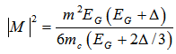
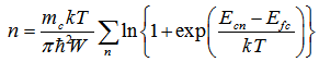
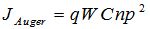
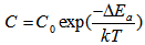
 , respectively.In high temperatures leakage current density becomes important [5]
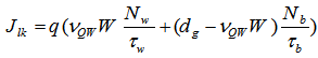 | (27) |
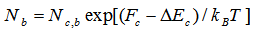 | (28) |
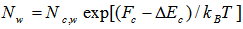 | (29) |
 life time of electrons above the barriers;Peak material gain multiply by optical confinement factor will result in peak mode gain. Optical confinement factor is a portion that shows the confinement of optical mode in active region that depends on the structure of the device. For our structure, optical confinement factor is taken from [2], 0.009 respectively.As described in [2] the mode gain-current density characteristic can be estimated by McIlroy formula (14). So using (14), we obtain mode gain-current density plots for three different barrier compositions in 25℃ and 85℃ [21].
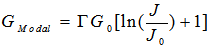 | (30) |
 optical confinement factor;We can also calculate the optimum gain per quantum well with McIlroy formula [21], Total threshold gain is calculated by the fact that in threshold gain should be equal with total losses [22]
 | (31) |
3. Simulation and Results Discussions
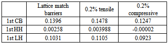
- Figure 3 shows the material gain-photon energy plot for three different barrier compositions ,as it is obvious the compressive strain barriers has the best gain spectra that it has more quantity in peak and the peak gain photon energy is about 0.956 eV that it is closer to 1.3µm wavelength photon energy.The first peak gain photon energy depends on the first conduction band energy level and the first heavy hole energy level. Table 2 shows the energy levels in these three situations.
|
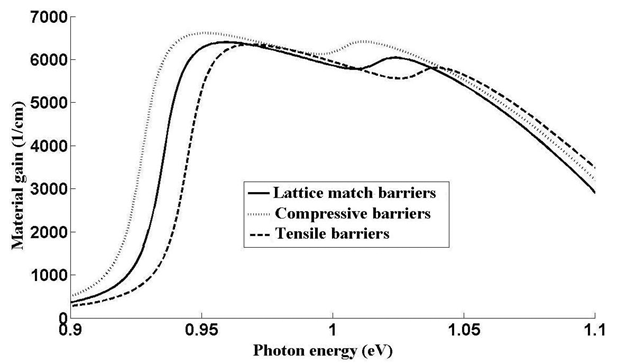 | Figure 3. Material gain Vs photon energy for different barrier strains |
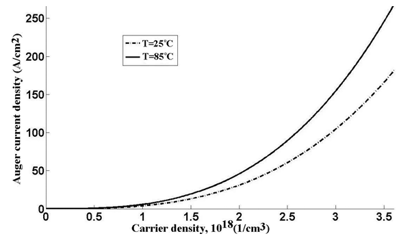 | Figure 4. Auger current density-carrier density characteristic in different temperatures |
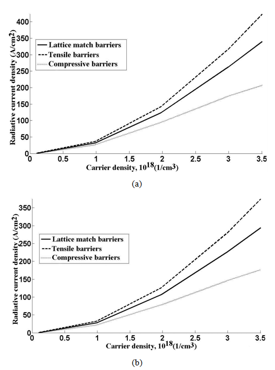 | Figure 5. Radiative current density-carrier density. (a)T=25℃. (b) T=85℃ |
 | (32) |
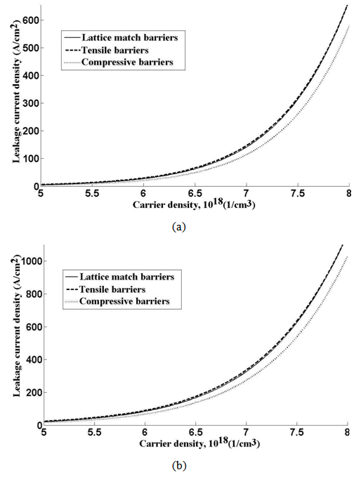 | Figure 6. Leakage current density-carrier density. (a) T=25℃. (b) T=85℃ |
 | (33) |
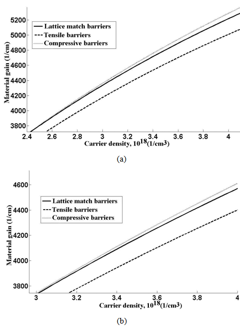 | Figure 7. Material gain-carrier density. (a) T=25℃. (b) T=85℃ |
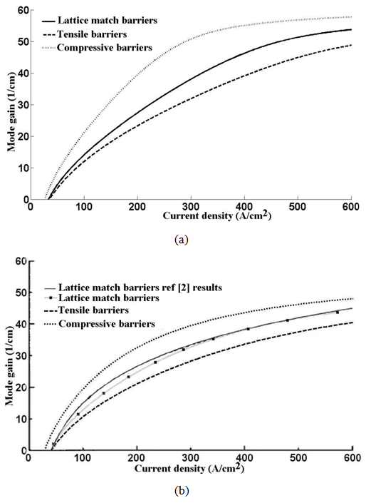 | Figure 8. Mode gain-current density. (a) T=25℃. (b) T=85℃ |
4. Conclusions
- In summary we have presented the background theory for optical gain and current density simulation of strained multiple quantum well lasers. We applied this theory to 1.3µm laser structure that was fabricated and presented in [2] with three different barrier compositions. In the lattice match barriers case simulations, good agreements have been obtained in comparison with results reported in [2]. For the first time we showed 0.2% compressive strain barriers in multiple quantum wells can make 20% improvement in mode gain-current density characteristic and 3% improvement in material gain spectra. Also Radiative, Auger and leakage current densities have been reduced significantly at higher temperature 85℃.
ACKNOWLEDGMENTS
- We would like to thank the Research Deputy of Amirkabir University of Technology for the research grant support. Also we thank Mr. Mohammad Sedghi for his role in editing and submission procedure of this paper.