-
Paper Information
- Next Paper
- Previous Paper
- Paper Submission
-
Journal Information
- About This Journal
- Editorial Board
- Current Issue
- Archive
- Author Guidelines
- Contact Us
International Journal of Optics and Applications
p-ISSN: 2168-5053 e-ISSN: 2168-5061
2014; 4(2): 31-39
doi:10.5923/j.optics.20140402.02
Optical Properties of Micro and Nanostructured Bioinspired Materials
 Abstract
 Reference
 Full-Text PDF
 Full-text HTML
Abdessitir Deraoui, Kamel Mallat, Alain Cornet, Pierre Defrance
Institute of Condensed Matter and Nanoscience (IMCN)/Nanophysics (NAPS), Université Catholique de Louvain Belgium
Correspondence to: Abdessitir Deraoui, Institute of Condensed Matter and Nanoscience (IMCN)/Nanophysics (NAPS), Université Catholique de Louvain Belgium.
| Email: |  |
Copyright © 2014 Scientific & Academic Publishing. All Rights Reserved.
The nature shows us a great many situations where the optics plays a crucial part; this is particularly the case for birds and insects whose color is usually associated with their behavior as a factor of recognition. This variation of coloration depends on the illumination and depending on the direction of observation: it is the phenomenon of iridescence. The material forming for example the elytra of beetles is the chitin and its refractive index is close to that of ordinary glass. The SEM observation shows that the material is in the form of multilayer separated by layers of air. These layers disturb the refractive index of chitin and cause multiple reflections which interfere and explain the phenomenon of iridescence. The models clearly confirm this interpretation [1], but they also show that it is possible to produce structured surfaces in the laboratory with properties similar to natural structures. By using design ideas from nature we are able to work towards the development of applications in a range of different technologies. This paper aims to develop methods for producing samples based on natural structures where optical properties can be interesting. We will review typical bio-inspired photonic structures and focus on the biomimetic fabrications. These samples will be characterized by various methods in order to understand its properties.
Keywords: Optical Properties, Iridescence, Multilayer, Photolithography, Anisotropic Wet Etching, Structured Surfaces, Scatterometry
Cite this paper: Abdessitir Deraoui, Kamel Mallat, Alain Cornet, Pierre Defrance, Optical Properties of Micro and Nanostructured Bioinspired Materials, International Journal of Optics and Applications, Vol. 4 No. 2, 2014, pp. 31-39. doi: 10.5923/j.optics.20140402.02.
Article Outline
1. Introduction
- The physical origin of the coloration of insects has been suspected very early [2, 3] and directly confirmed by electron microscopy as soon as this technique was made available [4]. Since then, one- [5], two- [6] and even three-dimensional [7] photonic crystals have been shown to be responsible for the coloration of many living organisms [8].Structural colours created by multilayer are widely used in the animal kingdom for display and/or camouflage [9–11]. There are many mechanisms by which structural colours can be produced. All depend directly or indirectly on the fact that a particular piece of material scatters or refracts different wavelengths of light to different degrees. This property of the material can be expressed in terms of its index of refraction, n, a measure of the degree to which a given wavelength of light entering the material is “retarded” or slowed down. Structural colours described so far in biological systems fall into two general classes, scattering and interference.The general category of interference includes those situations in which the rays of a beam of white light are temporarily separated and then brought back together in such a manner that some have traveled a longer path than others. Depending on the geometry, when the rays recombine, certain wavelengths are in phase and reinforced (“constructive interference”); these will shine with particular brilliance. Others are out of phase and cancel each other (“destructive interference”). The results are the shimmering colors we call “iridescent.” There are many ways of producing iridescence; this article considers only those of known importance in insects.It is now well known that submicron structures are responsible for the structural colour through light interference in layered or lattice structures and also Tyndall scattering [12].The physical structure and surface chemistry of these insects provides surprising properties that could offer a variety of applications ranging from photonic security tags to self cleaning surfaces and protective clothing and to industrial sensors.In this work, we created structures by etching periodic pyramid on surfaces of a flat sample of silicon and coated it with an alternating multilayer of the materials. The optical properties of the bio-inspired structures are also investigated.The combination of the nanofabrication technique, useful design methodologies inspired by biological systems would surely have profound impacts on our society.Subsequently, a theoretical model has been successfully proposed to explain the observed extraordinary reflective properties.
2. Material and Methods
- We wanted to fabricate a sample as shown in Fig.1 below. A pyramid with a base opening of D=100 μm and h=50μm of thickness (see Fig.1). We describe in detail in this paper the micro and nanofabrication steps made in the cleanrooms.
 | Figure 1. Design of the pyramid system |
2.1. Photolithography
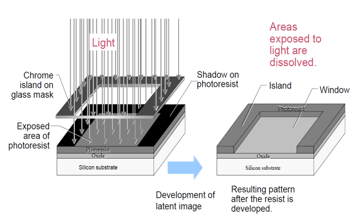
- Photolithography is the standard process to transfer a pattern, which has been designed with computer-aided- engineering (CAE) software packages, on to a certain material. The process sequence is illustrated in Fig.2 A mask with the desired pattern is created thanks to Cadence Virtuoso Layout Editor IC 5.0.0.
 | Figure 2. Schematic of a photolithographic process sequence to structure a thinfilm layer |
2.2. Anisotropic Wet Etching
- Liquid etchants etch crystalline materials at different rates depending upon which crystal face is exposed to the etchant. There is a large difference in the etch rate depending on the silicon crystalline plane. In materials such as silicon, this effect can allow for very high anisotropy. Some of the anisotropic wet etching agents for silicon are potassium hydroxide (KOH), ethylenediamine pyrocatechol (EDP), or tetramethylammonium hydroxide (TMAH). Etching a (100) silicon wafer would result in a pyramid shaped etch pit as shown in Fig.3. The etched wall will be flat and angled. The angle to the surface of the wafer is 54.7°.
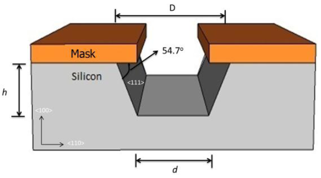 | Figure 3. Anisotropic wet etching a (100) silicon wafer |
 | (1) |
2.3. The Coating
- In order to produce the precise visual effect observed on ‘Chrysochroa vittata’, the structure is copied. The chitin plate (n=1.56) will be replaced by a layer of silicon monoxide SiO (n=1.9) and the nickel Ni (n=1.85) replaced the air layer. The purpose of choosing nickel is simply to produce a periodic perturbation in order to pen the one-dimensional photonic gaps. The multilayer alternates a silicon monoxide layer 170nm thick with 10nm layer nickel spacer.The deposition of SiO was made by evaporation from an electrically heated (by Joule effect) tantalum crucible, and the coating of nickel was applied by the evaporation of the nickel cathode, impacted by accelerated electrons driven by the static magnetic field of a permanent magnet.And because we have several facets in our pyramidal sample, what explains that we didn’t have the same thickness on all facets. To determine experimentally the effect of variation of angles, we deposited the same multilayer on flat substrates placed on oblique supports of 45° with the rotating plate of the evaporator and we measured the thickness of the coating thanks to Dektak profiler.
2.4. Morphology Characterization
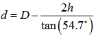
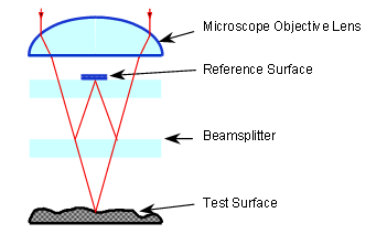
- A schematic of a coherence scanning interferometer is shown in fig.4 (left). The upper beam splitter directs light from the light source towards the objective lens. The lower beam splitter in the objective lens splits the light into two separate beams. One beam is directed towards the sample and one beam is directed towards an internal reference mirror. The two beams recombine and the recombined light is sent to the detector. Due to the low coherence of the white light source, the optical path length to the sample and the reference must be almost identical, for interference to be observed. Note that coherence is the measure of the average correlation between the value of a wave at any pair of times, separated by a given delay. Temporal coherence tells us how monochromatic a source is. In other words, it characterises how well a wave can interfere with itself at a different time (coherence is discussed in detail in the follow up guide discussed at the beginning of this chapter). The detector measures the intensity of the light as the interferometric objective is actuated in the vertical direction (z axis) and finds the interference maximum.
 | Figure 4. (Left) A typical Coherence scanning interferometry design. (right) Schematic of how to build up an interferogram on a surface using CSI. The vertical lines are intensity profiles at the image sensor |
 | Figure 5. Schematic of a Mirau interferometer |
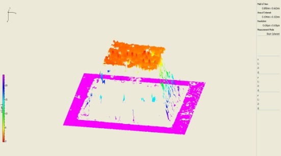 | Figure 6. 3D topography of the final design of sample measured by coherence scanning interferometry Polytec MSA-500 |
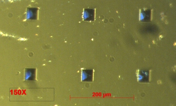 | Figure 7. Imaging microscopy of the structured surface of the bioinspired sample |
 | (2) |
 | (3) |
2.5. Optical Characterization
- The scatterometer we used in this work visualize the scattering patterns of small objects. The scatterometer measurements were helpful to understand the light scattering characteristics of pyramidal sample, and hence provide insight into sample coloration and its biological function. The power of the instrument is that it visualizes the near-field properties of the sample (with camera C1) (Fig.8), and simultaneously visualizes the far-field, hemispherical scattering properties of the study object (with camera C2). The imaging scatterometer consists of standard optical elements, except the ellipsoidal mirror. Mirror ellipsoid that it compresses a hemispherical space in a small cone, which then allows projection by common lenses. The system has an essential and sensitive point in that. The scattering of the sample must be exactly placed in the first focal point of the ellipsoid. In this have a practice is realized by observing the sample with the binocular viewer in which camera C1 is connected (bound), and besides by verifying that all the reflected light beams (shelves) cross (spend) a narrow diaphragm surrounding the second focal point, F2 (fig.8).
 | Figure 8. Diagram of the imaging scatterometer |
3. Results
3.1. Imaging Scatterometry
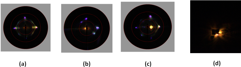
- The power of the imaging scatterometer was investigated on a small fragment of a highly iridescent bioinspired sample. The primary beam with aperture 5° was focused first on a flat surface of the sample and then on one of the pyramids, resulting in a 40 μm diameter spot (Fig.9) The near-field photograph shows the illumination of a small area, diameter about 40 mm, with the primary beam.
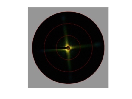 | Figure 9. Imaging scatterometry of flat surface of the sample. A small fragment was positioned in the scatterometer and the primary beam was projected as a 40 μm spot at a single scale |
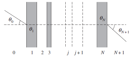
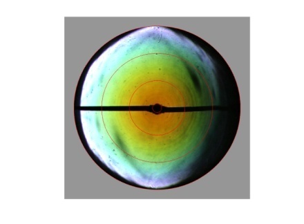 | Figure 10. Wide-aperture illumination yields scattering patterns that are orange in the centre and blue at large angles. The wider secondary light beam caused the additional scattering of the scale assembly |
 | Figure 11. Imaging scatterometry of one pyramid pattern a) Wide-aperture illumination yields scattering patterns with vertically linearly polarized Light b) Rotating the sample piece over angle of 5℃) Side illumination of a pyramid with a primary beam d) Wide-aperture side illumination yields scattering patterns The imaging scatterometer allows straightforward measurement of reflectance spectra. The incident light was scattered into a very wide angle (Fig.10). |
3.2. Detailed Modelling
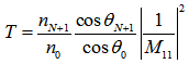
- The reflectance of the multilayer in our model was calculated by applying the classical multilayer theory for dielectric media.
 | Figure 12. Diagram of light propagation through a multilayer existing of N layers with refractive indices nj, = 1, 2, . . . , N, bordered by media with refractive index n0 and nN+1. The angles of light incidence and refraction at the interface of media j and j+1 are  and and  , respectively , respectively |
 , thicknesses of the layers
 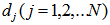 , their refractive indexes and extinction coefficients
  ; the imaginary part of the refractive index,
  , is related to the absorption coefficient of the medium,
  , by
, by  , where
  is the light wavelength. The propagation of light through this multilayer is governed by Snell’s Law:
 Where the angle of incident
  of the light ray at the interface of media j and j+1 can be complex. The light propagation through the multilayer is described by the transfer matrix
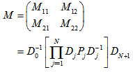 | (4) |
 | (5) |
 | (6) |
 for TE waves,
  and
and  for TM waves and sj = exp (
 ) with
  . The reflectance of the multilayer then is
 | (7) |
 | (8) |
 | (9) |
 and
and  To simulate the spectral response according to the wavelength, we modelled a pattern of pyramid with the same coating experimentally deposited, and by paying attention to the behavior of the variation of coating according to the angle of surface. Then, we simulated a white lighting to have the spectral response of the illuminated coating, and we observed the reflections when we send a package of the beams of light with the same power.
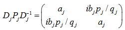
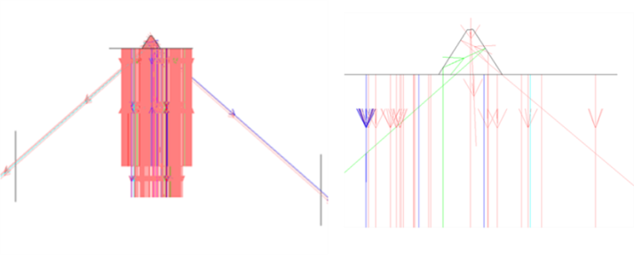 | Figure 13. Modelisation of a pyramid pattern |
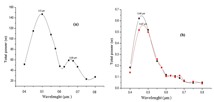 | Figure 14. Predicted reflectance of the bioinspired structure. a) with frontal detector b) with lateral detectors; red spectrum for the left detector and black spectrum for the right one |
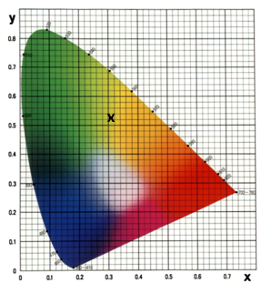 | Figure 15. Predicted colour of the bioinspired structurefrom the chromaticity diagrams |
 | (10) |
4. Conclusions
- The knowledge acquired in performing this study has been used to develop an artificial structured surface which reproduces the visual effect found with the Chrysochroa vittata beetle. In this insect, a combination of multilayer interference, optical gratings, photonic crystals and other optical structures gives rise to complex colour mixing. Although the physics of structural colours is well understood, it remains a challenge to create artificial replicas of natural photonic structures. O. Deparis et al.[25] and J.P. Vigneron et al.[1] used to develop also an artificial bio-inspired multilayer system which reproduces the visual effects provided by the insects cuticle. But our main goal in this work, is to analyze the role of roughness. We determined the optical properties changing of these structured surfaces based on the characteristics of surface roughness. We used a combination of pholithographic process, anisotropic wet etching, to fabricate pyramid structures on silicon subsrate, and we exploited the robustness of this thin-layer design, the changing colours of Chrysochora vittata were copied into a bio-inspired artificial reflector, with thin metal layers acting as periodic perturbation of a dielectric. Morphology characterization is used in this paper thanks to coherence scanning interferometry and stereomicroscopy and we measured the optical properties thanks to scatterometry technics. The measurements compared to theoretical modelling and numerical simulations will confirm the natural-artificial similarities.In this paper, we operated the strength of the surface roughness made by micro and nanofabrication to create the multiple reflections due to the internal surfaces of the pyramid to mimic or to produce samples based on natural structures where optical properties can be interesting. These Iridescent bio-inspired fabrications could find many uses in the hands of objects designers.
ACKNOWLEDGMENTS
- This investigation was conducted with the support of Communauté Française de Belgique through ARC project 10/15-033 “Propriétés optiques des structures naturelles et artificielles».We thank Prof. Doekele G. Stavenga for the scattering measures performed within the University of Groningen, Department of Applied Physics.