Hassan Kaatuzian1, Sadreddin Behjati Ardakani1, Mohammad Sedghi2
1Photonics Research Laboratory (PRL), Department of Electrical Engineering, Amirkabir University of Technology, Tehran, Iran
2Department of Electrical and Computer Engineering, Isfahan University of Technology, Isfahan, Iran
Correspondence to: Hassan Kaatuzian, Photonics Research Laboratory (PRL), Department of Electrical Engineering, Amirkabir University of Technology, Tehran, Iran.
| Email: |  |
Copyright © 2012 Scientific & Academic Publishing. All Rights Reserved.
Abstract
In recent years, effects that are concerned with quantum nature of light have attracted too attention. The more the devices become smaller, the quantum effects become more apparent. Single photon sources are the essential devices in many quantum information processes, such as quantum key distribution. One way for realization of single photon sources is to exploit quantum dots. Single quantum dot has the ability of single photon emission, which can be analyzed by quantum electrodynamics. Emission from quantum dots under special circumstances has non-classically effects. In present paper, first we extract a novel relation for computing optical absorption coefficient in k.p framework and three dimensional carrier confinements. Then with this relation, we analyze an electrically driven single photon source that its wavelength is more tunable in the fabrication process. This tunability is a consequence of exploiting a quantum dot surrounded by a quantum well. Eight-band k.p modeling is used for extracting of energy levels and spectral analyzing of quantum dot. In this work, we investigated theoretically, the emission from an InAs/InxGa1-xAs quantum dot. Using InxGa1-xAs alloy around the InAs provides us a freedom for tuning the source in a wide range of wavelengths. Eventually it is shown that for x=0.53, the peak gain occurs in 1.3µm wavelength which is used widely in fast fiber optic communication.
Keywords:
Single Photon Sources (SPSs), InAs/InxGa1-xAs Quantum Dot (QD), Optical absorption, Optical gain, Eight-band k.p modeling
Cite this paper: Hassan Kaatuzian, Sadreddin Behjati Ardakani, Mohammad Sedghi, Theoretical Analysis of Optical Absorption Coefficient Inside an InAs/InGaAs Semiconductor Quantum Dot Single Photon Source, International Journal of Optics and Applications, Vol. 4 No. 1, 2014, pp. 7-15. doi: 10.5923/j.optics.20140401.02.
1. Introduction
In our fast developing communication world, the thing highly demanded, is the security. Nowadays, the security of the information transportation in classical communication networks, is obtained by software programs and coding methods. If we require a highly secure method, we have to go towards quantum communications. According to no cloning theorem in quantum electrodynamics, if the state of a system is measured, the system does not no longer stay in own previous state and collapse to measured state. We can now exploit this feature of quantum nature of light by using for example polarization of photons as a quantum state. In this wonderful communication world, we will need Single Photon Sources (SPSs) for generating of single photons. Single photon emission is a non-classically feature of light that is described by quantum electrodynamics.The most promising things, which are capable of being SPS, are Quantum Dots(QDs).Because of three-dimensional carrier confinement in QDs[1], they have many amazing features, which have turned them to the center of attentions in many applications. Fabrication of QDs was one of the objections, which has solved in new technologies. Nowadays QDs are usually grown in self-assembled form, by MBE method in Stranski Krastanov (SK) mode. In this mode, after depositing several layers, islands begin to form. Single QD have the potential of emitting only one photon in each time; this property is the consequence of non-zero electron excitation time in QDs from ground state to the excited state. This promising feature of QDs is exploited for realization of SPSs.Another problem that is faced in realization of SPSs with QDs is the excitation method. The excitation can be electrical or optical. Electrical excitation has some advantages that distinguish it from optical ones, due to its controllability. Also in more cases, we need electrical modulation of signals.All the simulations and analyses in this paper based on k.p modeling. Depending on the size of QDs, we can use six or eight band approximation. k.p modeling gives us very good results specially around the band minima of direct semiconductors which is a favorite region in optoelectronics. The rest of the paper is organized in the following manner: In section 2, we describe the theory of k.p that is used for collecting the results. In section 3, we extract a novel relation for optical absorption coefficient in k.p framework and three dimensional carrier confinements. In section 4, we discuss about InAs/GaAs QDs and collect the results obtained from simulations. Our proposed structure and its results are then introduced in section 5.
2. Modeling by k.p Theory
The basic equation that should be solved in quantum mechanics problems is well-known Schrödinger equation. Energy levels and wave functions are obtained after solving of Schrödinger equation. Time independent Schrödinger equation is as follows: | (1) |
In this relation, is Hamiltonian of the system and is wave function. For a particle, Hamiltonian is defined as: | (2) |
 | (3) |
With these modifications, the simple one band Schrödinger equation is turned into a matrix eigenvalue problem. In wide bandgap semiconductors, that the coupling between electrons and holes is negligible, we can neglect conduction-valence band coupling, and therefore conduction band wave function can be obtained easily from the effective mass theory[2] by solving of the following equation: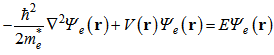 | (4) |
 is the electron’s effective mass that varies from material to material and subscript e means that the wave function belongs to electrons in conduction band. Valence band wave functions are obtained by solving of below matrix equation[3]:
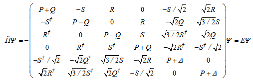 | (5) |
Where elements are as follows: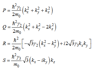 | (6) |
Moreover, Δ is the amount of spin orbit split-off energy, which depends on material. † stands for Hermitian conjugate. The parameters used in above relations are defined as follows: material dependent Luttinger constants,m0 : free electron mass,k: wave vector operator. In the cases, that confinement is in three directions, wave vector operator obeys below relation:
 | (7) |
 is gradient operator and subscripts in k indicate the direction of wave projection vector.Small size of QDs causes coupling of conduction and valence bands. Then finding of wave functions and energy levels reduces to the problem of diagonalization of an eight-order kohn-luttinger Hamiltonian[4], of the below form:
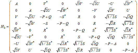 | (8) |
Parameters that their name is the same as previous are defined as before. Additional parameters are defined as follows: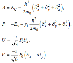 | (9) |
P0 is coupling between conduction and valence bands, it is convenience to define another parameter EP : | (10) |
Ec, Ev are conduction and valence band energies, respectively. As it can be seen, we added subscripts to Hamiltonian, which means that this Hamiltonian is in unstrained case. In presence of lattice mismatch between heterojunction materials, because of the strain, an additional matrix should be added to the Kohn-Luttinger Hamiltonian as in the following is shown[5]: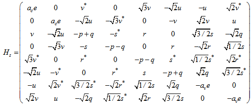 | (11) |
Where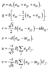 | (12) |
Parameters that are used are as follows:eij : strain tensor elements,b and d : the shear deformation potentials,av : hydrostatic valence band deformation potential,ac : hydrostatic conduction band deformation potential.Therefore total Hamiltonian for diagonalization is: | (13) |
If we approximate derivatives by finite differences, and repeat this procedure for all points in the system space, we will obtain an 8N×8N sparse matrix which N is the number of points in each direction. Therefore, the problem is reduced to diagonalizing of a sparse matrix, which there are some fast algorithms such as lanczos algorithm[6] .
3. Absorption Calculation
A useful quantity in optoelectronics is absorption or gain spectra of device. The optical absorption coefficient can be extracted from the below relation: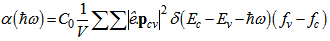 | (14) |
where: | (15) |
δ stands for Dirac delta function. The parameters used in the above relations are:V: volume of the considered structure; : unit vector in direction of polarization of incident light;  : Momentum matrix elements;Ec, Ev: energy levels in conduction and valence bands, respectively;fc, fv : Fermi Dirac distribution function in conduction and valence bands, respectively;
  : Electron charge, refractive index of material, speed of light, vacuum permittivity and free electron mass, respectively.If we write wave functions in the form of complex linear combination of basic wave functions then we have:
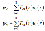 | (16) |
Where subscripts c and v stand for conduction and valence bands respectively; F's are envelope functions and ui's are basic wave functions. We can write momentum matrix elements according to our previous work in[7]: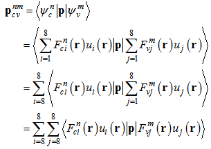 | (17) |
In the above relation we encounter to the term like this:  , because of slow varying envelope function over unit cells, we can approximate the aforementioned term by:
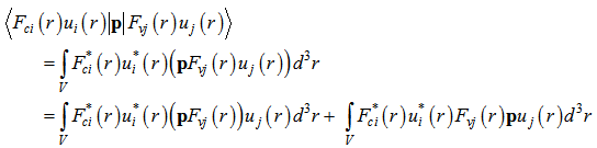 | (18) |
In this stage of manipulation, we use an approximation that can be proved in the following manner: If we have two functions F and G, so that F is a slow varying envelope function and G is a fast varying function over a unit cell, then for the integration of multiplication of two functions we have: | (19) |
On the above relation Ω stands for volume of a unit cell and all the integrations are over the whole volume.If we use this appropriate approximation in equation (18), we will have: | (20) |
Where, the  is the Kronecker Delta function and UC means unit cell. In extractions of above equation, we use the orthonormal property of basic functions, in bellow form:
 | (21) |
We named  as
as  ; which is known for all crystals[8]. With these approximations momentum matrix elements are seen in the form of:
 | (22) |
where: | (23) |
The term  is the overlap integral of envelope and can be calculated diagonalizing of k.p Hamiltonian.
4. Single Photon Emission
The structure that is usually used as electrically driven single photon emitter is PIN diode and an array of self-assembled QDs are grown inside the intrinsic region. The existence of intrinsic layer is necessary for generation of excitons[9], which their recombination leads to generation of photons. Since fabrication of single QD is difficult, therefore we must use a thin insulating AlOx aperture to select one QD among many of them for electrically excitation by current injection. In an experimental work, QDs in form of InAs surrounded by the GaAs alloy have been reported[10]. However, in this paper we are theoretically suggesting a new structure for improving the absorption spectra of the fabricated device reported in[10]. A simple scheme for the whole structure is depicted in figure 1. As it is shown, the whole structure is made of GaAs. InAs islands are grown in intrinsic region. Parameters of materials used in the simulations are tabulated in table 2. In All simulations in this work, we assume the temperature is set to 15K. 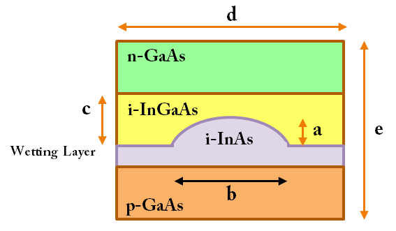 | Figure 1. a simple schematic m SPS, that is used in our simulations |
First we simulated a structure shown in figure 1 with the parameters gathered in Table 1 except for the c,–which is c=0 for this primarily study. In section 5, we will study our proposed structure with nonzero value of c parameter. Table 1. Structure parameters
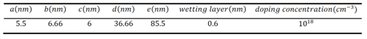 |
| |
|
Table 2. Physical parameters of materials used in simulations. These parameters is calculated in 15K
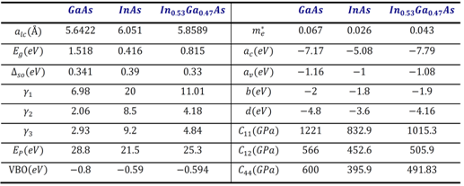 |
| |
|
After simulation of this structure by using the extracted absorption relation, we obtained the absorption spectrum of structure for both TE and TM polarization as shown in figure 2. This figure shows that the peaks occur around 1µm and 1.1µm that are dramatically matched with the results of the experimental work in[10] having similar parameters. The first peak is consequence of recombination in GaAs region and the second peak is due to the QD.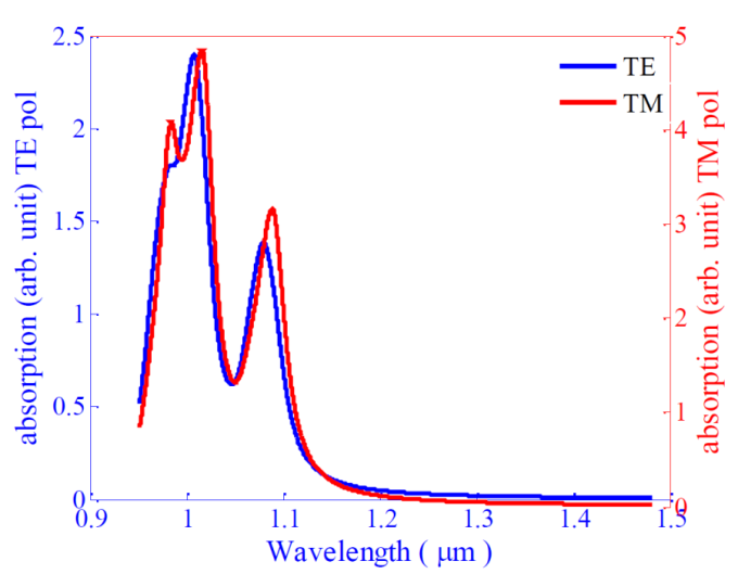 | Figure 2. absorption spectrum of InAs/GaAs QD |
With this structure–i.e. the c parameter is equal to zero, we cannot achieve wavelengths greater than 1.1µm and thus we cannot use this single photon emitter in fiber optic communications utilizing the common single mode fibers. In the following section, we introduce a new modified structure in which the wavelengths can be greater than 1µm.
5. The Proposed Structure for Single Photon Emitter
We know that the strain affects the bandgap of semiconductor such that compressive strain increases bandgap and tensile strain reduces it[11]. Thus, we exploit this property of strain for modifying the bandgap of InAs dot. In InAs/GaAs, heterojunction according to lattice constants in table 2, we have about 7% compressive strain, and therefore increasing of InAs bandgap and this by itself reduces the wavelength of emitted photons. For decreasing of bandgap, we need to reduce the compressive strain in heterojunction. For inclining to this important target, we proposed using of a strain reducing InxGa1-xAs layer around the InAs QD.Therefore transition between InAs QD and GaAs substrate is graded by structure which is depicted in figure 1, by lengths tabulated in table 1. All needed physical parameters are listed in table 1. It is worth noting that physical parameters of InxGa1-xAs alloy are calculated by interpolation, such that if G is a parameter then we have[12]: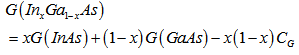 | (24) |
Where CG is bowing parameter related to G. For lattice and stiffness constants, we use simple linear interpolation. And temperature dependent energy gap is calculated from varshni’s model.In figure 3a, variation of InAs bandgap as a function of In fraction (x) of alloy is sketched. As it is expected, the slope of curve is negative. Figure 3b, shows variation of bandgap with respect to InGaAs layer height. As it is shown, increasing of this height leads to decreasing of bandgap; this is because of the fact that increasing of the height leads to reduction of strain. When the height of this layer exceeds the QD height, variations become slower. Figure 4, shows band diagrams of structure in different cases with or without doping and strain reducing layer along vertical direction that goes through the apex of QD.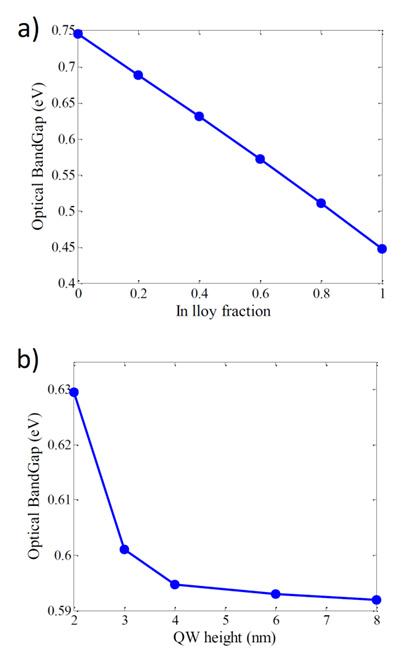 | Figure 3. variations of InAs bandgap as a function of a) In alloy fraction b) InGaAs height |
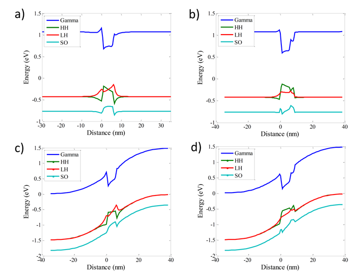 | Figure 4. band structure of system for a) absence of InGaAs layer (QW) and no doping b) existence of InGaAs layer but no doping c) absence of InGaAs layer but materials are doped d) existence of InGaAs layer and materials are doped |
So far, we have not applied any voltage across the diode and all of the results are about unperturbed structure. Here, we apply a voltage of 1.45 Volt across the diode for perturbing the structure. The existence of voltage is necessary for current injection to QD and therefore its excitation. Alternatively, for convenience it is possible to inject current into the diode for applying disturbance. In this circumstance, the gain spectrum is calculated for several values of different In alloy fraction. Eventually we find that for the case that In fraction is 0.53, the peak gain occurs at 1.3µm. Results are shown in figure 5, for both cases of existence and nonexistence of InGaAs layer and also for both TE and TM mode. These results are completely reasonable because any perturbation leads to energy level repulsion, and therefore energy difference between levels increases and leads to blue shift.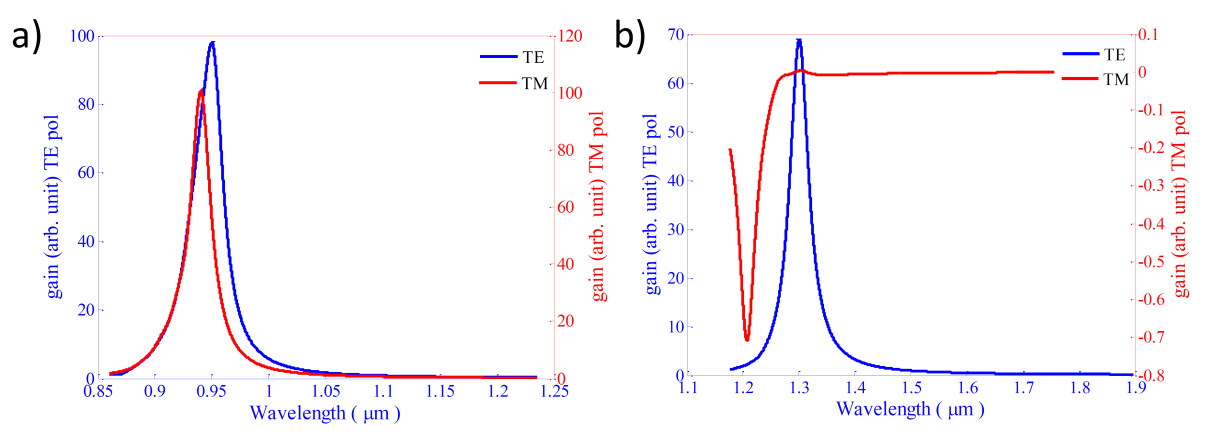 | Figure 5. gain spectra of QD a) with and b) without InGaAs layer. In both of cases, voltage drop across diode is 1.45 volt |
6. Conclusions
In this paper, first of all and in continuation of our previous work in[7], we extracted a novel formula for calculating of optical absorption coefficient in the k.p multiband framework with three dimensional carrier confinements. Next using this formula, we computed the absorption and gain spectra of a quantum dot single photon source. First, we simulated the InAs/GaAs quantum dot. We saw that in this case applying voltage across diode causes a peak gain at 950nm wavelength. It is not a suitable wavelength for common single mode fiber optic communications. Therefore, we modified the structure by exploiting of an InxGa1-xAs layer around the quantum dot. Simulation of this structure showed that for x=0.53, the peak gain occurs at 1.3µm.
References
| [1] | D. Bimberg, M. Grundmann, and N. N. Ledentsov, Quantum dot heterostructures vol. 471973882: John Wiley Chichester, 1999. |
| [2] | P. Harrison, Quantum wells, wires and dots: theoretical and computational physics of semiconductor nanostructures: Wiley-Interscience, 2005. |
| [3] | S. L. Chuang, Physics of optoelectronic devices, 2'nd ed. US: Wiley-Interscience, 1995. |
| [4] | C. Pryor, "Eight-band calculations of strained InAs/GaAs quantum dots compared with one-, four-, and six-band approximations," Phys. Rev. B, vol. 57, pp. 7190-7195, 1998. |
| [5] | M. Holm, "Theory and calculation of the electronic structure of strained InAs/InP quantum dots using the eight-band kp method," Master thesis, Lund University, 1999. |
| [6] | C. Galeriu, "k.p Theory of Semiconductor Nanostructures," Worcester polytechnic institute, 2005. |
| [7] | S. B. Ardakani and H. Kaatuzian, "Theoretical estimation of optical absorption coefficient inside an InAs/InGaAs semiconductor Quantum Dot," in Communications and Photonics Conference and Exhibition (Proc. of Optoelectronic Materials and Devices, and Asia Communications and Photonics (ACP)), 2011, Vol, 8308, pp. 1-6. |
| [8] | Y. Y. Peter and M. Cardona, Fundamentals of semiconductors: physics and materials properties: Springer, 2010. |
| [9] | H. Kaatuzian, Photonics, (In Persian), 3'rd ed. vol. 1. Tehran: Amirkabir University Press, 2012. |
| [10] | D. Bimberg, E. Stock, A. Lochmann, A. Schliwa, J. A. Tofflinger, W. Unrau, et al., "Quantum Dots for Single- and Entangled-Photon Emitters," Photonics Journal, IEEE, vol. 1, pp. 58-68, 2009. |
| [11] | V. B. Yekta and H. Kaatuzian, "Design considerations to improve high temperature characteristics of 1.3 μm AlGaInAs-InP uncooled multiple quantum well lasers: Strain in barriers," Optik - International Journal for Light and Electron Optics, vol. 122, pp. 514-519, 2011. |
| [12] | I. Vurgaftman, J. Meyer, and L. Ram-Mohan, "Band parameters for III–V compound semiconductors and their alloys," Journal of applied physics, vol. 89, pp. 5815-5875, 2001. |
 Abstract
 Reference
 Full-Text PDF
 Full-text HTML