-
Paper Information
- Next Paper
- Paper Submission
-
Journal Information
- About This Journal
- Editorial Board
- Current Issue
- Archive
- Author Guidelines
- Contact Us
International Journal of Optics and Applications
2012; 2(2): 1-5
doi: 10.5923/j.optics.20120202.01
All Optical Binary Divider
 Abstract
 Reference
 Full-Text PDF
 Full-Text HTML
Tamer A. Moniem
Faculty of engineering, MSA, Cairo-Egypt
Correspondence to: Tamer A. Moniem , Faculty of engineering, MSA, Cairo-Egypt.
| Email: |  |
Copyright © 2012 Scientific & Academic Publishing. All Rights Reserved.
This paper demonstrates numerically an all-optical binary divider and its optical control circuit for unsigned binary division by using all optical parallel shift register, optical logic gates and optical parallel adder. The concept is designed at an operation speed of 100 MHz for registers and 10 MHz for binary divider, which is limited by long laser cavities formed by the optical fiber.
Keywords: Optical Logic Gate, Optical Parallel Adder, Optical Central Processing Unit, Optical Flip Flop, Logic Divider, SOA
Article Outline
1. Introduction
- The emergence of increasingly high speed, digital optical system, and optical processing demands an all optical divider to executing a set of optical arithmetic micro-operations. The performing of signal processing operations entirely within the optical domain would exploit the speed and parallelism inherent to optics[1, 2].All-optical signal processing technologies are considered as a possible long-term route in the evolution of current telecommunication network and high-speed signal processing system[1]. In all-optical signal processing, all-optical binary divider is very important, which can have ultra-fast operating speed and eliminate the need of conversions between electronics and optics.The all optical Divider can be constructed with an optical arithmetic unit depicted in ref.[2], and an optical parallel-shift register[3,5] based on cascaded optical flip-flop memories driven by common optical clock pluses. The optical flip-flop memory consists of two coupled polarization switches[4,5] sharing an all-optical DeMultiplexer (DMUX 1*2), Multiplexer, all optical ADC[6], optical ALU[2,10], optical multiplier[5], and all optical divider depicted in this paper can be used in the arithmetic operation to perform a fast central processing unit using optical hardware components. Ultra-compact optical flip-flops with a switching speed greater than 100 GHz were demonstrated[7]. This means that this concept has potential to be integrated and to perform at high speed.
2. Theoretical Description of Division
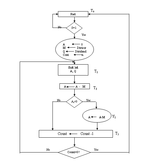
- Binary division is simpler than decimal division because the quotient digits are either 0 or 1 and there is no need to estimate how many times the dividend or partial remainder fits into the divisor. When the division is implemented in a digital computer, it is convenient to change the process slightly. Instead of shifting the divisor to the right, the dividend, or partial remainder, is shifted to the left, thus leaving the two numbers in the required relative position[8].
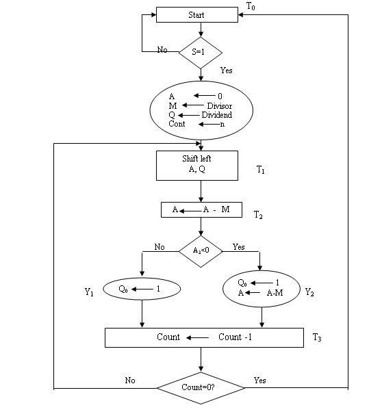 | Figure 1. The ASM flowchart of unsigned binary number |
3. The Optical Hardware Implementation for Binary Divider
- Due to the lack of reliable optical logic devices, the signal processing technology used in current optical packet switched cross-connects and optical processing is based on a combination of electronic and optical technology[5]. The all-optical arithmetic operation such as multiplier and divider is carried out in electronics while the payload remains in the optical domain, where the over-all operation is implemented using all-optical hardware components. All optical divider have many potential applications in optical communication systems and optical computing which lead to construct an all-optical central processing unit.This section describes an all-optical circuit that performs division of two binary optical words of 4 bits and could be used with all optical multiplier[5] for applications such as packet header processing and used in the construction of optical central processor unit.The register configuration for the all optical binary divider is shown in Figure 2. The divisor is stored in register (M), the result of division is stored in register (Q) and the remainder is formed in register (A). The registers Q, and M are formed by an all optical register using optical D flip flops[5, 9] which designed before in ref.[5]. The register A is formed by an all optical parallel-shift register according to the all optical binary multiplier in ref.[5]. A binary all optical parallel adder[2, 10] is employed for subtracting the content of register (A) to the content of register (M).
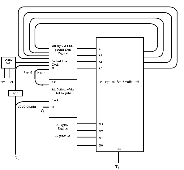 | Figure 2. All optical equipments configuration of optical divider |
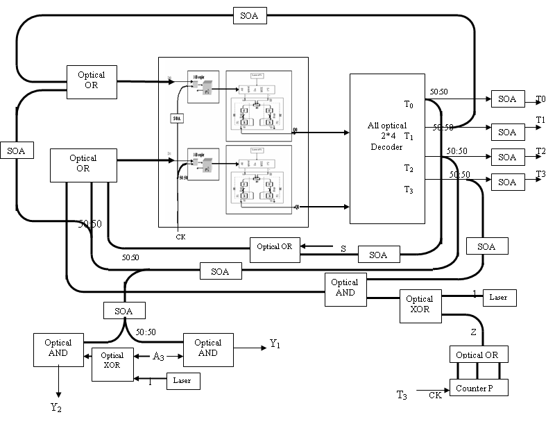 | Figure 3. All optical Control Circuit for unsigned binary divider |
3.1. The Optical Hardware of Divider Control Circuit
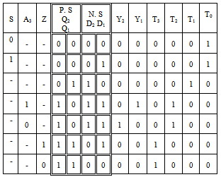
- The control circuit of binary divider is considered as a sequential circuit, its control lines are depicted in the ASM chart shown in figure 1. The control lines T0, T1, T2, and T3 are chosen for the state boxes, the control lines Y1, and Y2 are chosen for the conditional boxes, finally there are three decision boxes S, A3, and Z (Count=0). The state transition table of the control circuit according to the ASM flowchart is depicted in Table 1.
|
 | (1) |
 | (2) |
 | (3) |
 | (4) |
 | (5) |
 | (6) |
 | (7) |
 | (8) |
3.2. Simulation Results of Optical Unsigned Binary Division
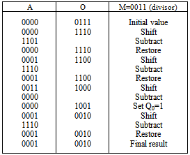
- The numerical example is depicted in table 2 to clarify the proposed division process. The divisor is stored in register M, and the double length dividend is stored in register A and Q.
|
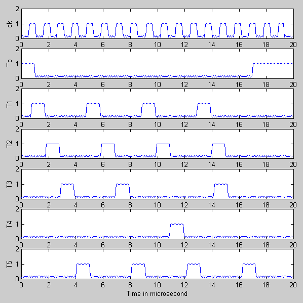 | Figure 4. Simulation result waveform of the control signals T0, T1, T2, T3 |
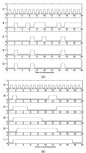 | Figure 5. (a) Simulation results waveform of Register A. (b) Simulation results waveform of Register Q and Zero flag Z Divider |
3.3. All Optical Signed Binary Divider
- The proposed all optical divider can be used also for the division of signed numbers except the setting of Qo=1 step is eliminated from the overall process of flow chart as shown in figure 6[14].
 | Figure 6. The ASM flowchart for signed binary number |
4. Conclusions
- An all-optical binary divider and its all-optical control circuit of unsigned binary division based on all optical parallel shift register at an operation of 10MHz to100 MHz, all-optical arithmetic unit based on the design of ref.[10] are designed and proven using the numerically simulated (Beam propagation method V.5) at an operation of 1MHz to 10 MHz for the overall division process.All-optical system computation eliminates the conversion from optical to electrical and vice versa. Accordingly, the latency is smaller than that using electrical digital computation. The time taken by each all-optical digital device is reduced to sub nanoseconds by building integrated Bragg gratings and optical fibers on SOI ridge waveguides[13, 7], where the optical integrated circuit processing is going to fabricate the fiber Bragg grating, SOA, TOAD elements, optical amplifiers and all optical digital circuits using the semiconductor devices[15, 16]. The operation speed may increase to perform a fast optical central processing unit by using the photonic integration, which would decrease the dimensions of the building blocks.
Acknowledgments
- The author would like to express his great thanks for Prof. Elsayed M. Saad and the late prof. M. K. Ahmed.
References
| [1] | D. Cotter, R. J. Manning, K. J. Blow, A. D. Ellis, et al., Science 286, 1523 (1999). |
| [2] | Tamer A. Rahman, Mohamed K. Ahmed and El Sayed M. Saad. “All-Optical Arithmetic-Logic Unit”.WSEAS Trans. On computer.ISSue 7, Volume 6, pp 985-990, July 2007. |
| [3] | S. Zhang, Z. Li, Y. Liu, G. D. Khoe and H. J. S. Dorren” Optical shift register based on an optical flip-flop memory with a single active element” . Vol. 13, No. 24, OPTICS EXPRESS. PP 9708-9713.Nov. (2005) |
| [4] | Y. Liu, M.T. Hill, H. de Waardt, G.D. Khoe, D. Lenstra, H.J.S. Dorren. “All optical flip-flop memory based on two polarization switches”. Electron. Lett. 38 (2002) pp 904-905 |
| [5] | Tamer A. Moniem, Nabil Abd Rabou, and E. M. Saad.” Parallel-shift register and binary multiplier using optical hardware components”, International SPIE optical engineering journal Vol 47, No3. March 2008. |
| [6] | K. Ikeda, J. Abdul, S. Namiki, ans K. Kitayama,”Optical Quantizing and coding for ultrafast A/D conversion using nonlinear fiber optic switches based on sagnac interferometer” Optic express, Vol 13, issue 11, PP. 4296-4302 (2005) |
| [7] | M. T. Hill, H. J. S. Dorren, T. J. de Vries, X. J. M. Leijtens, J. H. den Besten, E. Smalbrugge, Y. S. Oei, G. D. Khoe, and M. K. Smit, “A fast low-power optical memory based on coupled micro-ring lasers”. Nature 432, pp 206-209 (2004). |
| [8] | M.Morris Mano. ” Computer engineering hardware design”. prantice Hall international 1988. |
| [9] | Y. Liu, M.T. Hill, H. de Waardt, G.D. Khoe, D. Lenstra, H.J.S. Dorren. All optical flip-flop memory based on two polarization switches. Electron. Lett. 38 (2002) pp 904-905 |
| [10] | Tamer A. Rahman, Mohamed K. Ahmed and El Sayed M. Saad.”All optical arithmetic unit based on the hardlimiters”, in 6th WSEAS conference-corfu-Greece, pp 64-67, Feb2007. |
| [11] | Tamer A. Rahman, Mohamed K. Ahmed and El Sayed M. Saad." All-Optical Digital Full Adder, Decoder and Multiplexer by using Hardlimiters". in ICSES conference, Lodz- Poland, pp 775-778 Sep. 2006. |
| [12] | L. Brzozowski, and Edward H."A11- optical analog to digital converters, hardlimiters, and logic gates," IEEE J. lightwave technology, vol 19, pp 114-119, Jan 2001. |
| [13] | T. Murphy, T. Hastings, and H. Smith ,Fabrication and Characterization of Narrow-Band Bragg-Reflection Filters in Silicon on Insulator ridge wave guides, IEEE J. lightwave technology. PP.1938-1942, December 2000. |
| [14] | M.Morris Mano. ” Computer system architecture”.3rd edition, prantice Hall international 1993. |
| [15] | H. Nishihara, Masamitsu Haruna and Toshiaka Suhara"optical integrated circuit",1989, McGraw Hill. |
| [16] | Behzad Razavi, "Design of Integrated Circuits for Optical Communications", McGraw-Hill,2002. |