| [1] | Kimerling, L. C., Dal Negro, L., Saini, S., Yi, Y., Ahn, D.; Akiyama, S., Cannon, D., Liu, J., Sandland, J. G., Sparacin, D., Michel, J., Wada, K., Watts, M. R., 2004, Silicon Photonics: Topics in Applied Physics, Springer, Berlin. |
| [2] | Jalali, B., and Fathpour, S., 2006, Silicon Photonics, J. Lightwave Technol., 24(12), 4600-4615. |
| [3] | Rowe, L. K., Elsey, M., Tarr, N. G., Knights, A. P., Post, E., 2007, CMOS-compatible optical rib waveguides defined by local oxidation of silicon, Electron. Lett., 43(6), 392-393. |
| [4] | Vivien, L., Pascal, D., Lardenois, S., Marris-Morini, D., Cassan, E., Grillot, F., Laval, S., Fedeli, J. M., El Melhaoui, L., 2006, Light injection in SOI microwaveguides using high-efficiency grating couplers, J. Lightw. Technol., 24(10), 3810-3815. |
| [5] | Xu, Q., Manipatruni, S., Schmidt, B., Shakya, J., Lipson, M., 2007, 12.5 Gbit/s carrier-injection-based silicon micro-ring silicon modulators, Opt. Express, 15(2), 430-436. |
| [6] | Michael, C. P., Borselli, M., Johnson, T.J., Chrystal, C., Painter, O., 2007, An optical fiber-taper probe for wafer-scale microphotonic device characterization, Opt. Express, 15(8), 4745-4752. |
| [7] | Liu, A., Jones, R., Cohen, O., Hak, D., Paniccia M., 2006, Optical amplification and lasing by stimulated Raman scattering in silicon waveguides, J. Lightw. Technol., 24(3), 1440-1445. |
| [8] | Liu, A., Liao, L., Rubin, D., Nguyen, H., Ciftcioglu, B., Chetrit, Y., Izhaky, N., Paniccia, M., 2007, High-speed optical modulation based on carrier depletion in a silicon waveguide, Opt. Express, 15(2), 660-668. |
| [9] | Schares, L., Schow, C., Doany, F., Schuster, C., Kash, J., Kuchta, D., Pepeljugoski, P., Schaub, J., Trewhella, J., Baks, C., John, R., Shan, L., Hegde, S., Kwark, Y., Rogers, D., Libsch, F., Budd, R., Chiniwalla, P., Rosner, J., Tsang, C., Patel, C., Kucharski, D., Guckenberge, D., Dangel, R., Offrein, B., Tan, M., Trott, G., Nystrom, M., Tandon, A., Lin, C.K., Dolfi, D., 2005, “Terabus” - A waveguide based parallel optical interconnect for Tb/s-class on-board data transfer in computer system. Proc. of 31st European Conference on Optical Communications, 3, 369-372. |
| [10] | Kartalopoulos, S.V., 2002, Elastic bandwidth, IEEE Circuits Devices, 18, 8-13. |
| [11] | Schaub, J.D., Li, R., Csutak, S.M., Campbell, J.C., 2001, High-speed monolithic silicon photoreceivers on high resistivity and SOI substrates, J. Lightw. Tech., 19, 272-278. |
| [12] | Fan, H. Y., and Ramdas, A. K., 1959, Infrared Absorption and Photoconductivity in Irradiated Silicon, Journal of Applied Physics, 30, 1127-1134. |
| [13] | Wertheim, G. K., 1957, Energy Levels in Electron-Bombarded Silicon, Phys. Rev., 105, 1730. |
| [14] | Hill, D. E., 1958, Ph.D. thesis, Purdue University. |
| [15] | Longo, T. A., 1957, Ph.D. thesis, Purdue University. |
| [16] | Fan, H. Y., and Lark-Horovitz, K., 1958, Effects of radiation on Materials, Harwood, Hausner, Morse and Rauch: New York. |
| [17] | Lark-Horovitz, K., 1951, Semi-Conducting Materials, H. K. Henisch: London. |
| [18] | Wertheim G. K., 1958, Neutron-Bombardment Damage in Silicon, Phys. Rev., 111, 1500-1505. |
| [19] | Loferski, J. J., and Rappaport, P., 1958, Radiation Damage in Ge and Si Detected by Carrier Lifetime Changes: Damage Thresholds, Phys. Rev., 111, 432-439. |
| [20] | Geis, M. W., Spector, S. J., Grein, M. E., Schulein, R.T., Yoon, J. U., Lennon, D. M., Wynn, C. M., Palmacci, S. T., Gan, F., Kärtner, F. X., Lyszczarz, T. M., 2007, All silicon infrared photodiodes: Photo response and effects of processing temperature, Opt. Express, 15, 16886-16895. |
| [21] | Libertino, S., Coffa, S., Benton, J. L., Halliburton, K., Eaglesham, D. J., 2001, Formation, evolution and annihilstion of interstitial clusters in ion implanted Si, Phys. Rev. B, 63, 195206. |
| [22] | Harrick, N. J., 1962, Optical Spectrum of the Semiconductor Surface States from Frustrated Total Internal Reflections, Phys. Rev., 125, 1165. |
| [23] | Samoggia G., Nuciotti A., Chiarotti G., 1996, Optical Detection of Surface States in Ge, Phys. Rev., 144, 749. |
| [24] | Chiarotti, G., Del Signore, G., Nannarone, S., 1968, Optical Detection of Surface States on Cleaved (111) Surfaces of Ge., Phys. Rev. Letters, 21, 1170. |
| [25] | Allen, F. C., and Gobeli, G. W., 1962, Work Function, Photoelectric Threshold, and Surface States of Atomically Clean Silicon, Phys. Rev., 127, 150. |
| [26] | Garcia-Moliner, F., and Rubio, J., 1969, A new method in the quantum theory of surface states, J. Phys. C: Solid State Phys., 2, 1789. |
| [27] | Bortolani, V., Calandra, C., Sghedoni, A., 1971, Surface states in Si, Phys. Letters A, 34, 193. |
| [28] | Schocley, W., 1939, On the Surface States Associated with a Periodic Potential., Phys. Rev., 56, 317-323. |
| [29] | Chiarotti, G., Nannarone, S., Pastore, R., Chiaradia, P., 1971, Optical Absorption of Surface States in Ultrahigh Vaccum Cleaved (111) Surfaces of Ge and Si, Physical Review B, 4, 3398-3402. |
| [30] | Fowler, R. H., 1931, The analysis of photoelectric sensitivity curves for clean metals at various temperatures, Phys. Rev., 38, 45-56. |
| [31] | Vickers, V. E., 1971, Model of schottky barrier hot-electron-mode photodetection, Appl. Opt., 10, 2190-2192. |
| [32] | Chan, E. Y., Card, H. C., Teich, M. C., 1980, Internal Photoemission Mechanism at interfaces between Germanium and Thin Metal Films, IEEE J. Quantum Electron., 16, 373-381. |
| [33] | Scales, C., and Berini, P., 2010, Thin-film Schottky barrier Photodetector Models, IEEE Journal of Quantum Electronics, 46(5), 633-643. |
| [34] | Sze, S. M., 1981, Physics of Semiconductor Devices; John Wiley & Sons, New York. |
| [35] | Yuan H. X., and Perera, A. G. U., 1995, Dark current analysis of Si homojunction interfacial work function internal photoemission far-infrared detectors, Appl. Phys. Lett., 66, 2262-2264. |
| [36] | Boggess, T. F., Bohnert, K. M., Mansour, K., Moss, S. C., Boyd, I. W., Smirl, A. L., 1986, Simultaneous measurement of two-photon coefficient and free-carrier cross section above the bandgap of crystalline silicon, IEEE J. Quantum Electron., 22, 360-368. |
| [37] | Reintjes J. F., McGroddy, J. C., 1973, Indirect two-photon transitions in Si at 1.06 μm, Phys. Rev. Lett., 30, 901-903. |
| [38] | Reitze, D. H., Zhang, T. R., Wood, W. M., Downer, M. C., 1990, Two-photon spectroscopy of silicon using femtosecond pulses at above-gap frequencies, J. Opt. Soc. Am. B, 7, 84-89. |
| [39] | Tsang, H. K., Wong, C. S., Liang, T. K., Day, I. E., Roberts, S. W., Harpin, A., Drake, J., Asghari, M., 2002, Optical dispersion, two-photon absorption and self-phase modulation in silicon waveguides at 1.5 μm wavelength, Appl. Phys. Lett., 80(3), 416-418. |
| [40] | Cowan, A. R., Rieger, G. W., Young, J. F., 2004, Nonlinear transmission of 1.5 µm pulses through single-mode silicon-on-insulator waveguide structures, Opt. Express, 12, 1611-1621. |
| [41] | Dinu, M., Quochi, F., Garcia, H., 2003, Third-order nonlinearities in silicon at telecom wavelengths, Appl. Phys. Lett., 82, 2954-2956. |
| [42] | Dinu, M., 2003, Dispersion of phonon-assisted nonresonant third-order nonlinearities, IEEE J. Quantum Electron., 39, 1498-1503. |
| [43] | Bristow, A. D., Rotenberg, N., van Driel H. M., 2007, Two-photon absorption and Kerr coefficients of silicon for 850-2200 nm., Appl. Phys. Lett., 90, 191104. |
| [44] | Euser, T. G., Vos, W. L., 2005, Spatial homogeneity of optically switched semiconductor photonic crystals and of bulk semiconductors, J. Appl. Phys., 97, 043102. |
| [45] | Garcia H., and Kalyanaraman, R., 2006, Phonon-assisted two-photon absorption in the presence of a dc-field: the nonlinear Franz-Keldysh effect in indirect gap semiconductors, J. Phys. B, 39, 2737-2746. |
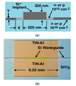
| [46] | Knights, A., House, A., MacNaughton, R., Hopper, F., 2003, Optical power monitoring function compatible with single chip integration on silicon-on-insulator Proc. of conference on Optical Fiber Communication, Technical Digest Series, 2, 705-706. |
| [47] | Bradley, J. D. B., Jessop, P. E., Knights, A. P., 2005, Silicon waveguide-integrated optical power monitor with enhanced sensitivity at 1550 nm, Appl. Phys. Lett., 86, 241103. |
| [48] | Knights, A. P., Bradley, J. D., Gou, S. H., Jessop, P. E., 2006, Silicon-on-insulator waveguide photodetector with self-ion-implantation-engineered enhanced infrared response, J. Vac. Sci. Technol. A, 24, 783-786. |
| [49] | Liu, Y., Chow, C. W., Cheung, W. Y., Tsang, H. K., 2006, In-line channel power monitor based on helium ion implantation in silicon-on-insulator waveguides, IEEE Phot. Technol. Lett., 18, 1882-1884. |
| [50] | Giri, P. K., and Mohapatra, Y. N., 2000, Thermal stability of defect complexes due to high dose MeV implantation in silicon, Mater. Sci. Eng., 71, 327-332. |
| [51] | Geis, M. W., Spector, S. J., Grein, M. E., Schulein, R. T., Yoon, J. U., Lennon, D. M., Denault, S., Gan, F., Kaertner, F. X., Lyszczarz, T. M., 2007, CMOS-compatible all-Si high-speed waveguide photodiodes with high responsivity in near-infrared communication band, IEEE Photon. Technol. Lett., 19, 152-154. |
| [52] | Geis, M. W., Spector, S. J., Grein, M. E., Yoon, J. U., Lennon, D. M., Lyszczarz, T. M., 2009, Silicon waveguide infrared photodiodes with >35 GHz bandwidth and phototransistors with 50 AW-1 response, Opt. Express, 17, 5193-5204. |
| [53] | Shafiiha, R., Zheng, D., Liao, S., Dong, P., Liang, H., Feng, N., Luff, B. J., Feng, D., Li, G., Cunningham, J., Raj, K., Krishnamoorthy, A. V., Asghari, M., 2010, Silicon waveguide coupled resonator infrared detector. Proc. of Optical Fiber Communication Conference, 21–25. |
| [54] | Almeida, V. R., Barrios, C. A., Panepucci, R. R., Lipson, M., Foster, M. A., Ouzonnov, D. G., Gaeta, A. L., 2004, L-optical switching on a silicon chip, Opt. Lett., 29, 2867-2869. |
| [55] | Baehr-Jones, T., Hochberg, M., Walker, C., Scherer, A., 2004, High-Q ring resonators in thin silicon-on-insulator, Appl. Phys. Lett., 85, 3346-3347. |
| [56] | Little, B. E., Chu, S. T., Haus, H. A., Foresi, J., Laine, J. P., 1997, Microring resonator channel dropping filters, J. Lightw. Technol., 15, 998-1005. |
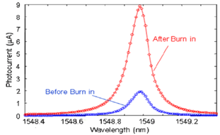
| [57] | Doylend J. K., Jessop P. E., Knights A. P., 2010, Silicon photonic resonator-enhanced defect-mediated photodiode for sub-bandgap detection, Opt. Express, 18, 14671-14678. |
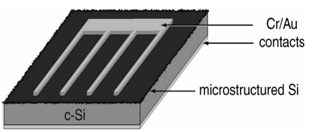
| [58] | Wu, C., Crouch, C. H., Zhao, L., Carey, J. E., Younkin, R., Levinson, J. A., Mazur E., Farrell, R. M., Gothoskar, P., Karger, A., 2001, Near-unity below-band-gap absorption by microstructured silicon, Appl. Phys. Lett., 78, 1850-1852. |
| [59] | Carey, J. E., Crouch, C. H., Shen, M., Mazur. E., 2005, Visible and near-infrared responsivity of femtosecond-laser microstructured silicon photodiodes, Opt. Lett., 30, 1773-1775. |
| [60] | Baehr-Jones, T., Hochberg, M., Scherer, A., 2008, Photodetection in silicon beyond the band edge with surface states, Opt. Express, 16, 1659-1668. |
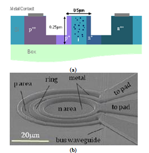
| [61] | Chen, H., Luo, X., Poon, A. W., 2009, Cavity-enhanced photocurrent generation by 1.55 µm wavelengths linear absorption in a p-i-n diode embedded silicon microring resonator, Appl. Phys. Lett., 95, 171111. |
| [62] | Kosonocky, W. F. , Shallcross, F. V., Villani, T. S., 1985, 160x244 Element PtSi Schottky-Barrier IR-CCD Image Sensor, IEEE Trans. Electron Dev., ED-32( 8), 1564. |
| [63] | Casalino, M., Sirleto, L., Moretti, L., Della Corte, F., Rendina, I., 2006, Design of a silicon RCE schottky photodetector working at 1.55 micron, Journal of luminescence, 121, 399-402. |
| [64] | Casalino, M., Sirleto, L., Moretti, L., Della Corte, F., Rendina, I., 2006, Design of a silicon resonant cavity enhanced photodetector based on the internal photoemission effect at 1.55 µm. Journal of Optics A: Pure and applied optics, 8, 909-913. |
| [65] | Casalino, M., Sirleto, L., Moretti, L., Rendina, I., 2008, A silicon compatible resonant cavity enhanced photodetector working at 1.55 μm, Semicond. Sci. Technol., 23(7), 075001. |
| [66] | Elabd, H., Villani, T., Kosonocky, W. F., 1982, Palladium-Silicide Schottky-Barrier IR-CCD for SWIR Applications at Intermediate Temperatures, IEEE Trans. Electron Devices Lett., EDL-3, 89-90. |
| [67] | Lee, M. K., Chu, C. H., Wang Y. H., 2001, 1.55-µm and infrared-band photoresponsivity of a Schottky barrier porous silicon photodetector, Opt. Lett., 26(3), 160-162. |
| [68] | Casalino, M., Sirleto, L., Moretti, L., Gioffrè, M., Coppola, G., Rendina, I., 2008, Silicon resonant cavity enhanced photodetector based on the internal photoemission effect at 1.55 µm: Fabrication and characterization, Appl. Phys. Lett., 92(25), 251104. |
| [69] | Casalino, M., Coppola, G., Gioffrè, M., Iodice, M., Moretti, L., Rendina, I., Sirleto, L., 2010, Cavity enhanced internal photoemission effect in silicon photodiode for sub-bandgap detection, J. Lightw. Technol., 28(22), 3266-3272 |
| [70] | Casalino, M., Sirleto, L., Iodice, M., Saffioti, N., Gioffrè, M., Rendina, I., Coppola, G., 2010, Cu/p-Si Schottky barrier-based near infrared photodetector integrated with a silicon-on-insulator waveguide, Appl. Phys. Lett., 96(24), 241112. |
| [71] | Zhu, S., Yu, M. B., Lo, G. Q., Kwong, D. L., 2008, Near-infrared waveguide-based nickel silicide Schottky-barrier photodetector for optical communications, Appl. Phys. Lett., 92(8), 081103. |
| [72] | Zhu, S., Lo, G. Q., Kwong, L., 2008, Low-cost and high-gain silicide Schottky-barrier collector phototransistor integrated on Si waveguide for infrared detection, Appl. Phys. Lett., 93(7), 071108. |
| [73] | Zhu, S., Lo, G. Q., Kwong, D. L., 2008, Low-Cost and High-Speed SOI Waveguide-Based Silicide Schottky-Barrier MSM Photodetectors for Broadband Optical Communications, IEEE Phot. Tech. Lett., 20(16), 1396-1398 |
| [74] | Reather, H., 1988, Surface Plasmons on Smooth and Rough Surfaces and on Gratings. Springer, Berlin. |
| [75] | Ebbesen, W., Lezec, H. J., Ghaemi, H. F., Thio, T., Wolff, P. A., 1997, Extraordinary optical transmission through sub-wavelength hole arrays, Nature, 391, 667-669. |
| [76] | Barnes, W. L., Dereux, A., Ebbesen, T. W., 2003, Surface plasmon subwavelength optics. Nature, 424(6950), 824–830. |
| [77] | Maier A., 2006, Plasmonics: Fundamentals and Applications. Springer, New York. |
| [78] | Scales, C., and Berini, P., 2004, Schottky Barrier Photodetectors, U. S. Patent No. 7,026,701. |
| [79] | Scales, C., Breukelaar, I., Berini, P., 2009, Surface-plasmon Schottky contact detector based on a symmetric metal stripe in silicon, Opt. Lett., 35(4), 529–531. |
| [80] | Scales, C., Breukelaar, I., Charbonneau, R., Berini, P., 2011, Infrared Performance of Symmetric Surface-Plasmon Waveguide Schottky Detectors in Si, IEEE J. Lightw. Tech., 29(12), 1852-1860. |
| [81] | Akbari A., and Berini, P., 2009, Schottky contact surface-plasmon detector integrated with an asymmetric metal stripe waveguide, Appl. Phys. Lett., 95(2), 021104. |
| [82] | Akbari, A., Tait, R. N., Berini, P., 2010, Surface plasmon waveguide Schottky detector, Opt. Express, 18(8), 8505- 8514. |
| [83] | Olivieri, A., Akbari A., and Berini, P., 2010. Surface plasmon waveguide Schottky detectors operating near breakdown, Phys. Status Solidi RRL, 4(10), 283 – 285. |
| [84] | Goykhman, I., Desiatov, B., Khurgin, J., Shappir, J., Levy U., 2011, Locally Oxidized Silicon Surface-Plasmon Schottky Detector for Telecom Regime, Nano Lett., 11, 2219–2224. |
| [85] | Tsang, H. K., and Liu, Y., 2008, Nonlinear optical properties of silicon waveguides, Semicond. Sci. Technol., 23, 064007. |
| [86] | Liang, T. K., Tsang, H. K., Day, I. E., Drake, J., Knights, A. P., Asghari, M., 2002, Silicon waveguide two-photon absorption detector at 1.5 µm wavelength for autocorrelation measurements, Appl. Phys. Lett., 81, 1323-1325. |
| [87] | Bravo-Abad, J.; Ippen, E.P.; Soljačić, M. Ultrafast photodetection in an all-silicon chip enabled by two-photon absorption. Appl. Phys. Lett. 2009, 94, 241103. |
| [88] | Tanabe, T., Sumikura, H., Taniyama, H., Shinya, A., Notomi, M., 2010, All-silicon sub-Gb/s telecom detector with low dark current and high quantum efficiency on chip, Appl. Phys. Lett., 96, 101103. |
| [89] | Akahane, Y., Asano, T., Song, B. S., Noda, S., 2003, High-Q photonic nanocavity in a two-dimensional photonic crystal, Nature, 425, 944-947. |
| [90] | Tanabe, T., Nishiguchi, K., Kuramochi, E., Notomi, M., 2009, Low power and fast electro-optic silicon modulator with lateral p-i-n embedded photonic crystal nanocavity, Opt. Express, 17, 22505-22513. |
| [91] | Chen H., and Poon, A. W., 2010, Two-photon absorption photocurrent in p-i-n diode embedded silicon microdisk resonators. Appl. Phys. Lett., 96, 191106. |
| [92] | Kikuchi, K., 1998, Highly sensitive interferometric autocorrelator using Si avalanche photodiode as two-photon absorber. IEEE Elec. Lett., 34, 123-125. |
| [93] | Kikuchi, K., 1998, Optical sampling system at 1.5 µm using two photon absorption in Si avalanche photodiode. IEEE Elec. Lett., 34, 1354-1355. |
| [94] | Salem, R., and Murphy, T. E., 2004, Polarization-insensitive cross correlation using two-photon absorption in a silicon photodiode, Opt. Lett., 29, 1524-1526. |
| [95] | Tanaka, Y., Sako, N., Kurokawa, T., 2003, Profilometry based on two-photon absorption in a silicon avalanche photodiode, Opt. Lett., 28, 402-404. |
| [96] | Shi, B., Liu, X., Chen, Z., Jia, G., Cao, K., Zhang, Y., Wang, S., Ren, C., Zhao, J., 2008, Anisotropy of photocurrent for two-photon absorption photodetector made of hemispherical silicon with (110) plane, Appl. Phys. B, 93, 873-877. |
| [97] | Sheperd, F. D., Vickers, V. E., Yang, A. C., 1971, Schottky Barrier Photodiode with a Degenerate Semiconductor Active Region, U.S. Patent No. 3.603.847. |
 Abstract
 Reference
 Full-Text PDF
 Full-text HTML
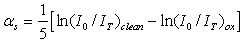
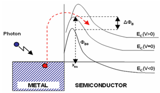
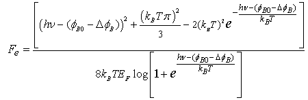
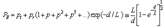
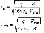


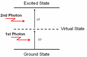
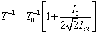
 is a coefficient taking into account the probability that the two-photon absorption process occurs. It is clear that in conventional linear optics, the absorption cross section σ is a constant. Atomic transition rate R, due to two-photon absorption, scales as the square of the laser intensity, is shown in the following formula:

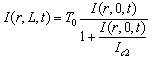
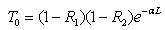
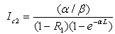
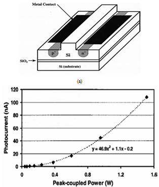
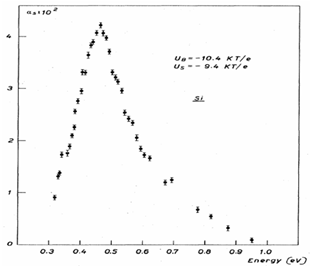
 plane, on which aluminum electrodes were evaporated. The electrodes consisted of concentric circular and annular metal contacts with a spacing of 0.15 mm and a radius of 0.5 mm for the central electrode. The contacts between the aluminum and the silicon hemisphere are considered to be ohmic contacts. Because TPA substantially occurs in the vicinity of the focused spot (the center of the hemisphere), the concentric electrodes collect the photo-excited carriers efficiently.The responsivity of the detector was about 2 μA/W at 1300 nm and 1 V of applied bias. This silicon photodetector is easy to fabricate and is useful in autocorrelation for measuring ultra-short laser pulses with wavelengths in the region of 1.2–2.1 μm.