-
Paper Information
- Previous Paper
- Paper Submission
-
Journal Information
- About This Journal
- Editorial Board
- Current Issue
- Archive
- Author Guidelines
- Contact Us
International Journal of Optics and Applications
p-ISSN: 2168-5053 e-ISSN: 2168-5061
2011; 1(1): 8-12
doi: 10.5923/j.optics.20110101.02
Implementation of 1-Bit Random Access Memory Cell in All-Optical Domain with Non-linear Material
 Abstract
 Reference
 Full-Text PDF
 Full-Text HTML
Samir Sahu 1, Radha Raman Pal 1, Shantanu Dhar 2
1Department of Physics and Technophysics, Vidyasagar University, Midnapore, 721102, India
2Department of Physics, Jhargram Raj College, Jhargram, 721507, India
Correspondence to: Samir Sahu , Department of Physics and Technophysics, Vidyasagar University, Midnapore, 721102, India.
| Email: |  |
Copyright © 2012 Scientific & Academic Publishing. All Rights Reserved.
This paper demonstrates an all-optical 1-bit Random Access Memory (RAM) with massive use of nonlinear material. All-optical switching mechanism is exploiting here to realize the all-optical 1-bit RAM. The all-optical switch by a composite slab of linear medium (LM) and non-linear medium (NLM) is the building block of our proposed 1-bit RAM circuit. An all-optical clocked D flip flop is the main storing element of the RAM. These circuits are simple and all-optical in nature. It can also gear up to the highest capability of optical performance in high-speed all-optical data storing, computing and communicating system.
Keywords: Nonlinear Material, All-Optical Switch, All-Optical D Flip-Flop, 1-Bit Read/Write Memory Cell, All-Optical RAM
Cite this paper: Samir Sahu , Radha Raman Pal , Shantanu Dhar , "Implementation of 1-Bit Random Access Memory Cell in All-Optical Domain with Non-linear Material", International Journal of Optics and Applications, Vol. 1 No. 1, 2011, pp. 8-12. doi: 10.5923/j.optics.20110101.02.
Article Outline
1. Introduction
- To cope with the explosive growth of the internet traffic, the expected necessity for parallel, ultrahigh speed, ultrahigh bandwidth, no crosstalk, low loss information processing[1] has provided remarkable impetus for understanding of all-optical devices and circuits[1-3]. Last few years have witnessed an enhanced weight in optical communication[3-4] and computing[5] due to some important advancement, namely, the development of laser, optical fiber and novel materials that exhibit high nonlinearities[1, 5-12]. These developments of optics offer tremendous scope to overcome the obstacle to implement various arithmetic[2, 7-8], logic[9-14, 18-20], algebraic[15] and image operations[16] in all-optical domain successfully. The advent of non-linear optical material based all-optical switching mechanism[1, 5-12, 18, 25] has opened exciting new possibilities for improvement of several new all-optical components of terahertz all-optical computer, our dream goal.This promising technique of all-optical switching can show its potential in combinational logic circuits[2, 7-8, 17] as well as sequential logic circuits[9-12, 18]. For examples, all-optical S-R, S-R with clock, D, J-K and J-K master-slave type flip-flops using non-linear material[9-12, 18-20], all optical register[11, 22-23], all optical counter[12] have been reported. Various all-optical memories have also been pro posed[22-24]. They are not as fast as to fulfil the demand ofnow-a-days. To gear up the performance speeds (storing speed and retrieving speed) we implement an all-optical 1-bit random access memory[21] which is constructed by the clocked D flip flop[9,11].This circuit can raise to a higher bit other types of RAM. As this 1-bit RAM is purely all-optical in nature, it is very simple as well as very fast. Also the scheme has capacity of cascading. These circuits are key elements for the implementation of a high-speed, all-optical data processing device, which has the potential to outperform its electronic equivalent and constitute a possible new product for next generation computation[1,5] and communication[3-4] to scale their capacity to the traffic demand.
2. Ultra Fast All-optical Switching behaviour of Nonlinear Material and their Application in All-Optical NOT Gate as well as AND Gate
- The phenomenon photorefractivity[6, 8-12] of some nonlinear optical material is used in nonlinear all-optical intensity switching mechanism. The refractive index[1, 6, 8-12, 25-27] of some nonlinear materials (NLM) such as carbon disulfide, pure silica, potassium dihydrophosphate (KH2PO4), (KDP) crystal etc. varies linearly with the intensity of the light incident on it. The refractive index (n) of such isotropic dielectric non-crystalline media can be put into an equation as in (1). Here n0 is the linear term, n1 is the nonlinear correction term and I is the intensity of the incident light beam on the material.
 | (1) |
2.1. Ultra Fast All-Optical Switching Behavior of Nonlinear Material
- We can implement the switching mechanism with such nonlinear material by taking an interface between two media of which one is a linear material (LM), whose refractive index n0 is independent of the intensity of light and the other is aforesaid NLM. A laser beam, highly intense polarized light, preferably pulse laser of intensity I1, is allowed to incident on the interface from linear to nonlinear part in a particular direction XO (incidence angle θ1) as depicted in Figure 1. The refracted beam from the NLM follows the path OZ. But when another higher intense laser beam of intensity I2 (I2> I1) is made to incident along XO, after refraction from the NLM the light passes through OY direction (angle of refraction θ2). The deviation of refractive angle for different incident light intensity I1 and I2 is
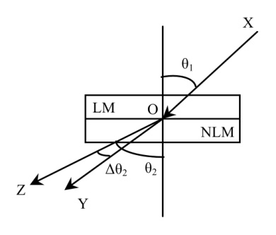 | Figure 1. Intensity switching of optical nonlinear material |
2.2. All Optical NOT Gate
- To implement an all optical NOT gate using non-linear material a constant intensity pulse laser source (CILS) is used as shown in Figure 2. It is also called probe beam. Here P1 is taken as input beam. A detector is placed at P2 will detect the output beam after refraction. If P1 is absent, the light will follow a path OP2 and will be detected by the detector due to presence of CILS. But if P1 is present, after refraction, the light will follow a path other than OP2, may be OP3, and the detector will not detect any light signal. Thus the system acts as optical NOT gate.
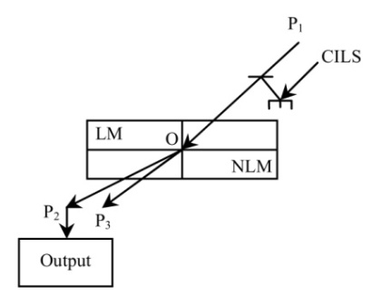 | Figure 2. All-optical NOT gate |
2.3. All Optical AND Gate
- The all-optical AND gate using two inputs and three inputs are shown in Figure 3. The two inputs all-optical AND gate using NLM is shown in Figure 3(a). Here R1 and R2 are two input channels. A detector placed at R4 gives the output. Now when both the channels carry light signal, the light beam after refraction will detected by the detector at R4, unless not.
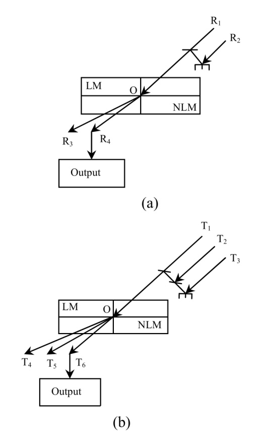 | Figure 3. All-optical AND gate using NLM. (a) two-input AND gate. (b) three-input AND gate |
|
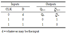
3. All-optical 1-bit Random Access Memory Cell
- We now describe the all-optical circuit of 1-bit random access memory (RAM) cell as shown in Figure 4. Here Di is the Data Input of the 1-bit RAM and D0 is the Data Output of the cell. There are two other inputs namely Address Select input (An) and Read/Write Control input (R/
 ). The main storing component of this RAM cell is the clocked D flip-flop[9, 11] shown in the dash box as in Figure 4. The truth table is depicted in Table 2. Except the D flip-flop, here we use one all-optical NOT gate (NG6) and two AND gates (AG5 and AG6). AG5 is a two-input AND gate while AG6 is a three-input AND gate. All the gates are based on optical nonlinear material as the basic building block of our proposed RAM cell. The R/
  input is complemented at the D10 terminal through NG6 due to the presence of probe beam CILS6. Now AG5 has An and D10 as two inputs and E11 as output. Again Data Input (Di) of the RAM cell is fed to D input of the D flip-flop and E11 is fed as clock (CLK) of the D flip-flop. The flip-flop has outputs Q and
  , complement to each other. An, R/
  and Q are the three inputs of the AND gate AG6. The output (F12) of AG6 is the final output (D0) of the proposed all-optical 1-bit Read/Write memory cell.
|
 and Di. Now CLK of the D flip-flop is absent which preserved the previous state (Qn+1 = Qn). So as long as An = 0, the input and output activities are blocked, and the cell is in the hold mode where its stored data is protected.(2) If Address Select input bears photon (An = 1), the cell is enabled for writing and reading operation. There are two possibilities.
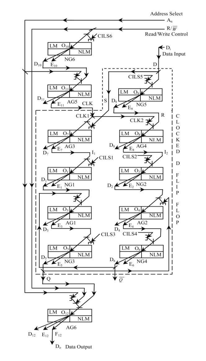 | Figure 4. All optical random-access memory cell using NLM as switch |
 is equal to 0. Then the output D0 (= F12, output of AG6) becomes 0 independent of Q. i.e. the output of the cell is detached from Q. One cannot read from the memory cell in this state. But light will follow the path O11E11 when passing through AG5 as both the input beams (An = D10 = 1) have light. Now the clock of the D flip-flop becomes at logical ‘1’ state. So the D flip-flop stores 0 if Di = D = 0 and writes 1 if Di = D = 1 according to Table 2. Therefore, if An = 1 and R/
  = 0, writing (storing) operation of single bit data (Di) is done into the memory cell.
|
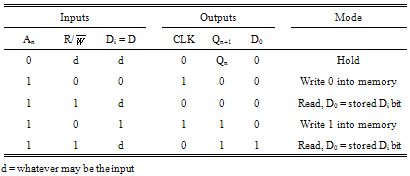
 as 1. There will be no light at E11 terminal as D10 = 0. Again the clock of the D flip-flop is absent. The flip-flop remain in its former output state ignoring D (= Di) input. In the present situation none can write into the memory cell. But for AG6, as two inputs (An = R/
  = 1) are at logically high state, the output follows the third input Q. That means Q comes out at D0 through O12F12 direction. Q is nothing but the stored Di bit. So we can conclude that stored digital data will be retrieved from 1-bit read/write memory cell when both the inputs An and R/
  transmit light.The function table is given in Table 3. All-optical 1-bit RAM cell can store digital optical data and retrieve it as desired. In our scheme we use all optical AND and NOT gate in designing the all optical 1-bit RAM cell. In our design the light beam which is fed back is coming from the output of a NOT gate. Again the concept used here to design the all optical NOT gate has an advantage. Whenever the output of a NOT gate is assumed to be at ‘1’ state, the source of that ‘1’ state is a constant intensity pulse laser source (CILS) used as probe beam. So in each feedback arrangement described in our scheme similar intense light beam is fed back. In this way the reduction of intensity by using beam splitter will not affect the non-linear response of the device. The light sources are so chosen that each input beam intensity is in the range of intensity which is detected as ‘1’ by the detector after refraction. The source of the final output (D0) of the RAM cell is CILS3. As long as the power is on, the stored data bit is protected and the data retrieval is possible. Therefore the proposed all-optical RAM cell can be used as volatile memory cell.
5. Conclusions
- The proposed technique of all optical implementation of all optical 1-bit RAM cell is very fast (above THz)[8-12, 26-27] as it is fully all-optical. It is volatile in nature. The storing and reading time of this memory cell will be in fs. The light signals which are severally used and the feedback light signals from the outputs are made by mirrors and beam splitters to make the circuits simple. Another important feature is that other higher order all-optical temporary data storage memories may be developed by cascading the cell. Other different types of memories can be implemented from this read/write memory cell. Proper findings of non-linear material[25-27] may be a significant issue here. Essentially inputs and constant intensity light source should be chosen properly to run the system accurately. The clock pulse signal should also be selected suitably.
ACKNOWLEDGEMENTS
- The authors want to acknowledge Professor Sourangshu Mukhopadhyay of the for his valuable suggestions.