E. A. Odo
Department of Physics, Federal University Oye-Ekiti, Oye-Ekiti, Nigeria
Correspondence to: E. A. Odo, Department of Physics, Federal University Oye-Ekiti, Oye-Ekiti, Nigeria.
| Email: |  |
Copyright © 2015 Scientific & Academic Publishing. All Rights Reserved.
Abstract
The morphology and elemental composition of silicon nanoparticles, produced by means of a vibratory disc mill in a top-down synthesis route has been investigated, using scanning electron microscopy (SEM), energy dispersive x-ray spectroscopy (EDX) and transmission electron microscopy (TEM). Both SEM and TEM reveals that the particles consisted of a wide range of size distributions, ranging from a few faceted particles about 1-3 μm in size, to a large number of much rounder particles in the 100nm range. This size distribution pattern fits in well with a log-normal distribution function, with a mean size being observed to shift to the lower particle size ranges with increasing milling time. The EDX analysis reveals that the level of contaminants, which may have resulted from reactions with the milling medium, as well as with the atmospheric oxygen, remains insignificant for the duration of the milling process.
Keywords:
Nanoparticles, Microscopy, Morphology
Cite this paper: E. A. Odo, Morphology and Elemental Study of Silicon Nanoparticles Produced Using a Vibratory Disc Mill, Nanoscience and Nanotechnology, Vol. 5 No. 3, 2015, pp. 57-63. doi: 10.5923/j.nn.20150503.02.
1. Introduction
Nanostructured materials have received much interest and intense research efforts in recent times because of their great potential for engineering and scientific applications [1]. Annexing such geometry scaling, and other novel properties of semiconductors at this length scale will lead to great improvement in electronic device performance [2]. The ability to produce silicon nanoparticles in large quantities, has accelerated the development of printed electronic devices on flexible substrates [3, 4]. One of the stark limitation to the application of bulk nanostructured materials, however, is their poor ability to provide fully dense and defect-free parts [1]. The route that is generally employed to circumvent this shortcoming in the production of isolated and uncontaminated nanostructured particles, is to use either inert gas condensation [5], or chemical reactions of a precursors. In the case of silicon, this has traditionally involved one of two forms of thermal processing: pyrolysis of silanes [6-9], or evaporation of bulk silicon in an inert atmosphere [10, 11]. Of these, two methods, the most widely used is the decomposition of silane gas, which can be achieved by using simple thermal pyrolysis [5] or laser decomposition [8], to produce particles with sizes in the range of 100nm. However, the application of soft chemical synthesis methods to create silicon nanoparticles, is limited by their complexity, as it involves multi-stage synthesis [12] or growth in inverse micelle structures, as well as by their low yield [13].The high cost and complexity of the above mentioned route limits its application, predominantly to the laboratory [14]. The “top-down” approaches, employing high energy mechanical milling or chemical reduction, which are widely used in the industrial production of metal and ceramic powders, have been successfully employed for silicon and other notable semiconductor materials too [15]. Mechanical milling in particular enables the low-cost production of nanostructured materials with the added advantage being simplicity and effectiveness. Many reports have however suggested, that mechanical milling of crystalline materials often results in particles that vary in size and structure, varying from isolated spherical particles to agglomerate of complex structures. Therefore, a major concern associated with this method is the control of the resulting physical features, such as the average diameter and morphology of the particles. Another concern is the possible contamination of the processed materials by the milling medium [16, 17].In this work, standard techniques SEM and TEM was used to investigate the propagation of morphological properties (size and shape) of silicon nanoparticles produced through mechanical attrition of silicon wafer by a vibrator disc mill. The elemental compositions of the produced particles, and the proliferation of the contaminants resulting from the milling process was also studied as a function of milling time.
2. Experimental Procedure
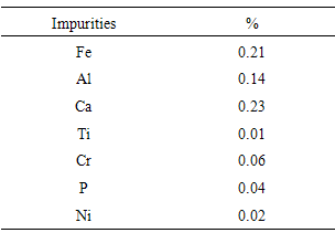
Batch milling of two types of bulk silicon was done by using a Siebtechnik 800W TS laboratory vibratory disc mill, equipped with a 52100 chrome steel pestle and mortar [18]. The bulk silicon sources used in this work were, p-type silicon wafers and, for comparison purposes, a metallurgical grade silicon (more specifically, a 2503 grade polycrystalline silicon metal), provided by Silicon Smelters (PTY) Ltd. Polokwane, South Africa. The purity of the p-type silicon wafer was nominally 99.99%, while the metallurgical grade silicon, according to the manufacturer’s analysis, contained 99.40% silicon. Table 1 lists the known elemental impurities constituting the remaining 0.60% of the metallurgical grade silicon. The milling process pulverized the materials by means of impact and friction, usually in a few minutes, while at the same time homogenizing the grounded powder. The first set of powder produced came from milling the silicon wafers for 1 hour through to 5 hours. The second set came from milling the metallurgical grade silicon for 3 hours.Table 1. Impurities listed by the producer of the metallurgical grade silicon
 |
| |
|
The morphology and the elemental composition of the nanostructured sets of powdered silicon produced above were studied using a Leica Stereoscan S440i scanning electron microscope (SEM). For imaging, the operating beam energy used was 20keV with a probe current of 50-100pA, which gave an estimated resolution for images of about 10nm in secondary electron mode. SEM micrographs of the different samples were taken from three different regions at magnifications ranging from relatively low (x10000) to higher (x50000) levels. Different areas of the samples were then examined for their elemental compositions, with a focus on silicon (as the primary constituent), oxygen, chromium and iron from possible contamination from the atmosphere and the milling medium. This was achieved by using a beam energy of 20keV and a beam current of 1000pA with a working distance of 25.0mm.Small quantities of each of the different powders were dispersed in ethanol contained in separate plastic bottles. The contents of the bottles were then sonicated in an ultra-sonic bath for 1 hour. This was to ensure that the clustered lumps were properly broken down and fully dispersed in the ethanol. Two drops each of the dispersed powders in the ethanol, were placed by means of a pipette on a carbon coated surface of a sample holder made of aluminum. The sample was then placed under a 100W electric bulb to vaporize the ethanol before measurements were taken.The transmission electron microscopy (TEM) study was carried out by using a LEO 912 transmission electron microscope, operating at 120keV. The samples for the TEM study were prepared by placing two drops, from each of the different powder dispersions in ethanol on holey (porous) carbon coated TEM grids. To ensure that enough particles were viewed for the particle size distribution analysis, pictures from four different areas of a given sample were taken at the same magnification and later merged at their common boundaries to produce a panoramic (wide view) micrograph.
3. Results and Discussion
Fig. 1 (a) - (e) are micrographs of the powder milled for 1-5 hours. The morphology and size distribution of the particles in the powder after an hour of milling as seen in Fig. 1 (a), shows that the powder consisted of particles with a wide range of sizes and two predominant shape type. On the one hand are large faceted particles, cleaved along closely packed planes, with sizes ranging from 1 – 3μm, and on the other hand are relatively smaller particles, with sizes ranging from 100 – 400nm with a generally spherical shape. The size distribution, based on a random measurement of 150 particles that have clearly defined boundaries along their longest axis, shows a typical log-normal distribution pattern. The more spherical particles (100 – 400nm) were found to dominate the distribution.After 2 hours of milling, the resulting powder exhibited a similarly wide size distribution pattern like that after 1 hour of milling. Comparing the two powder, the proportion of the particles in the size range of 100 – 400nm was observed to have increased after 2 hours. The average particle size was also observed to have shifted toward the lower numbers. Further milling of the powder up to 5 hours, (as seen in Fig. 1 (c) - (e)), shows a progressive increase in the proportion of the particles towards the size range of 100 – 400nm resulting from a consistent reduction of the larger faceted particles with milling time. Also worth mentioning is the presence of clustering of the smaller particles into super clusters of relative larger sizes. Fig. 1 (f) is a micrograph of the metallurgical grade silicon after it has been milled for 3 hours. It has a similar size distribution as the 3 hours milled powder produced from the wafer. Unlike the milled wafer powder that has large faceted particles in the size range 1 – 3μm, the larger particles, in this case are predominately spherical with smoother surfaces. 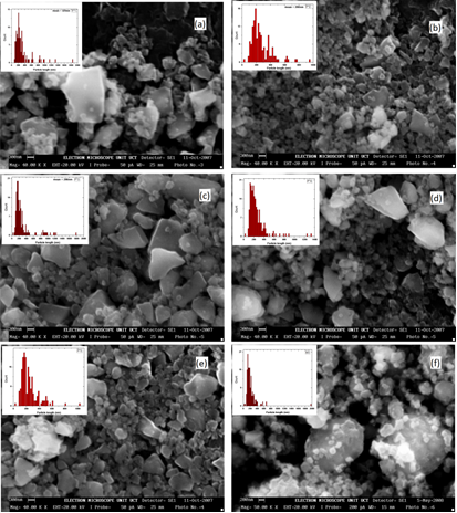 | Figure 1. SEM micrographs of milled silicon wafer after (a) 1 hour (b) 2 hours (c) 3 hours (d) 4 hours and (e) 5 hours milling, consisting of a wide range of sizes and two predominant shape type. The average particles size decreases with increasing milling time. (f) A 3 hours milled metallurgical silicon shows particles with wide range of sizes and predominately spherically shaped |
Fig. 2 shows the plot of the spectra intensity versus X-ray energy on a semi-log scale for the EDX analysis carried out on the 5 hours milled wafer powder. From the spectra, silicon at  is clearly the dominant element in the powder constituting about
  , with oxygen at
  , iron at
  and chromium at
  constituting only trace amounts in the powder. No clear peaks were found in the different energy positions indicated by the arrows, corresponding to the energy levels for the possible contaminants. The trace amount of contaminant detected within the instruments resolution is indicative that the contamination from the milling medium and the possible atmospheric oxidation from the milling process were insignificant.
 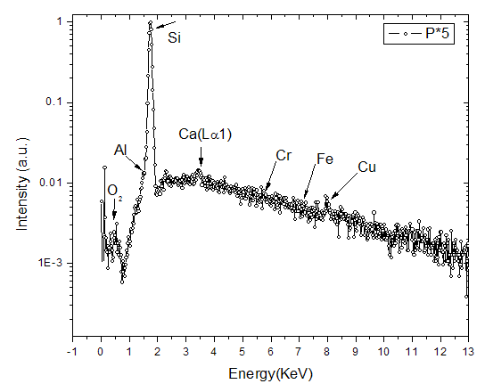 | Figure 2. EDX plot of spectra intensity versus X-ray energy for milled silicon powder after 5 hours on semi-log scale, showing silicon at 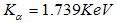 as the dominant element, with possible contaminants like oxygen, chromium and iron appearing in trace amount as the dominant element, with possible contaminants like oxygen, chromium and iron appearing in trace amount |
Fig. 3 shows the effect of milling time on the levels of the detected oxygen, chromium and iron, estimated from the spectra intensity of the EDX analysis carried out on the milled wafer samples milled from 1 to 5 hours using a standard software installation for the instrument. From the figure, oxygen appears to be the most contaminating element; this level of oxygen may be associated with an initial surface oxidation of the starting bulk wafer rather than any oxidation resulting during milling. since the oxygen level remains fairly constant throughout the period of milling. This reasoning is supported from the Raman spectroscopy study on both the bulk and milled powder reported in [19], where oxide phases were identified in both starting materials. The two other possible contaminants, chromium and iron, appears in trace amounts, with no considerable changes in their levels with changing milling time.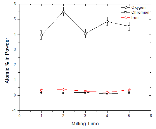 | Figure 3. Showing the levels in atomic % of detected oxygen, chromium and iron in the milled powder remaining relatively constant for the entire milling period |
Fig. 4 shows the TEM images at the same magnification for the powders from the milled silicon wafer (a) – (e) and the milled metallurgical silicon (f). The TEM micrograph for the 1 hour milled powder (see Fig. 4(a)), clearly shows that the powder is composed of large faceted particles whose cross-section are in the range of  . There are also scattered clusters of particles, consisting of the relatively smaller particles in the range of
  , where
  represents the length of the longest cross-section of the particle, with the smallest measured particle recorded, been
  .
. | Figure 4. TEM micrographs showing a continuous reduction from the larger faceted particles to smaller rounder particles, varying with increasing milling time for the milled wafer silicon powder, (a) 1 hour, (b) 2 hours, (c) 3 hours, (d) 4 hours, (e) 5 hours and (f) a larger distribution of more rounder shape of 3 hours milled metallurgical silicon powder |
A comparison of the 1 and 2 hours milled powders (see Fig. 4(a) and (b)) shows a clear reduction in the average particle sizes after 2 hours of milling. The distribution of particles in the 2 hours milled sample, shows a relative larger population of the smaller and predominantly spherical particles than those in the 1 hour sample as earlier observed in the SEM study. As the milling time reaches 5 hours, as seen in Fig. 4(e), the population of the smaller and spherically shaped particles in the size range of  becomes dominant.A closer look at a larger grain at higher magnification (Fig. 5) shows darker areas either overlaying or embedded in the particle (the areas indicated in the dotted circle). This may be the result of either the agglomeration and compacting of small particles into relatively bigger clusters due to the hammering process in the mill, or the result of plastic deformation of particle, thus giving rise to stacks of crystallites, with planes of orientation different to those of the initial material [19].
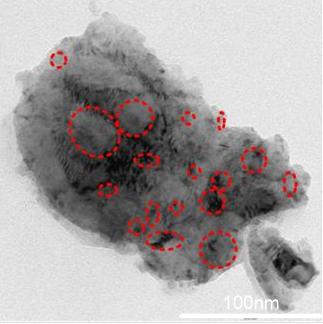 | Figure 5. TEM micrograph of a single large grain showing either an agglomeration of smaller particles or a possible stacking of re-oriented crystallites |
To quantify how the average particle size and hence the particle size distribution varied with milling time, each of the micrographs in Fig. 4(a) - (e) was analyzed by using an image processing software equipped with length measurement tools. The longest axis of each clearly identified (in other words, having well defined boundaries) particle or cluster was measured. For the purposes of this measurement, in regions where there were no clear boundaries, some of the clusters were taken as a single particle.Fig. 6 and 7 show the size distribution pattern of the 5 hours milled silicon wafer particles, and of the 3 hours milled metallurgical grade silicon powder respectively. The distribution of the measured cross-sectional lengths of the particles can be described by a log-normal function (1), with a peak center shifting to the lower particle cross-sectional region as the milling time increases.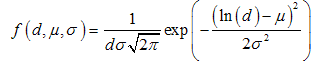 | (1) |
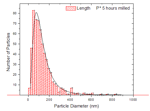 | Figure 6. Particle size distribution for powder 5 hours milled silicon wafer fits well to a log-normal pattern with a mean cross-section size of 113nm |
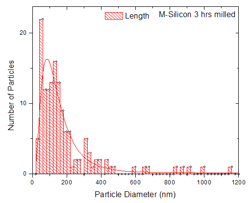 | Figure 7. Particle size distribution for milled metallurgical silicon powder showing a similar size distribution pattern as 5 hours milled wafer powder. It fits well to a log-normal function with a mean cross section size of 127nm |
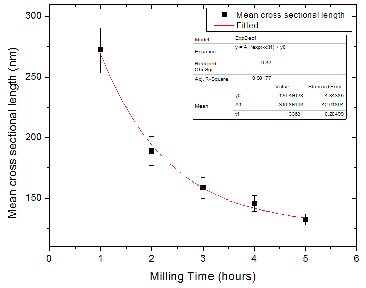 | Figure 8. The variation of the mean cross-sectional particle sizes for the milled wafer with increasing milling time |
In (1),  is the cross-sectional length of the particle,
  and
and  are the logarithmic mean and standard deviation respectively. The fit of this function to the size distribution histogram was used to derive a mean particle size for each of the milled powders. The center position of the fitted function, which corresponds to the average cross-sectional length, was plotted against milling time in Fig. 8. The plot shows a decrease in the average particle size with milling time, and this data can be well represented with a first order exponential decay function given as,
 | (2) |
Where  describes the particle diameter after milling for a time
  ,
,  is the initial particle diameter,
  defines a time constant and
  represents a constant size value for the particles diameter after a very long milling time.A fit of (2) to the data of Fig. 8 yields a value for
  . It is reasonable to conclude that this value represents the average cross-sectional size of particle that can be achieved after a long time of milling using this method. A similar analysis carried out on the metallurgical silicon powder can be adequately represented by a log-normal distribution function, centered at 96nm.From the above, it is reasonable to suggest that the production of silicon powder from a single crystalline silicon wafer, using a vibratory disc mill in a top-down synthesis route, starts with cleavage of the wafer along its preferred orientation, followed by a gradual attrition of the particles surfaces toward the smaller particle size, reaching a fairly constant size distribution after about 3 hours of milling. The effect of further milling only reduces more of the larger particles to the size range 100 nm – 400nm.The shape and size distribution, as observed for the five hours milling of the wafer is comparable to those obtained from high-energy ball milling of single crystalline silicon for 50 hours reported by Di-Guerra et. al [19]. This finding suggests that the present method is a fast and efficient method of producing silicon nanoparticles from its bulk state.While cleavage and later attrition is true for the wafers, this may not be the case for the metallurgical silicon. The differences in the surface texture of particles derived from the wafers, which have sharp edges, and those derived from the metallurgical silicon bulk, which have smoother round surfaces, suggests that the process of reduction in the metallurgical powder is due to attrition alone. However, the size distribution after 3 hours of milling is comparable in both systems.
4. Conclusions
In this study silicon nanoparticles were produced via a top-down synthesis route, from both single crystalline and a polycrystalline bulk form, using a laboratory disc mill. The milled silicon nanoparticles powders produced via this process showed a continuous reduction of particle size with milling time. In the case of powder from the single crystalline bulk (i.e. the wafers), the process started with cleavage along its main crystal orientation, followed by attrition of the edges of the particles as they became smaller. In the case of powders from the polycrystalline bulk, the reduction process appeared to be due to attrition alone. In general, the produced powders irrespective of the starting bulk materials were composed of an agglomeration of smaller particles, resulting in bigger clusters. The effect of milling time on the contaminant level was negligible. The detected oxygen level remained fairly constant for the entire milling period, suggesting minimal silicon oxidation from the process, and the measured value was most likely an intrinsic oxygen level that was already part of the bulk.
References
| [1] | X. Phung, J. Groza, E.A. Stach, L.N. Williams, S.B. Ritchey, Materials Science and Engineering A, 359 (2003) 261-268. |
| [2] | S.T. Lee, N. Wang, C.S. Lee, Materials Science and Engineering A,, 286 (2000) 16-23. |
| [3] | A. Reindl, C. Cimpean, W. Bauer, R. Comanici, A. Ebbers, W. Peukert, C. Kryschi, Colloids and Surfaces A, 301 (2007) 382-387. |
| [4] | A. Reindl, A. Voronov, P.K. Gorle, M. Rauscher, A. Roosen, W. Peukert, Colloids and Surfaces A, 320 (2008) 183-188. |
| [5] | K. Kim, D. Woo, J.-H. Park, S.-G. Doo, T. Kim, Journal of the Korean Physical Society, 54 (2009) 1021 - 1026. |
| [6] | K. Tonokura, T. Murasaki, M. Koshi, J. Phys. Chem. B., 106 (2002) 555 - 563. |
| [7] | V.G. Kravets, C. Meier, D. Konjhodzic, A. Lorke, H. Wiggers, J. Appl. Phys. , 97 (2005) 084306. |
| [8] | M. Ehbrecht, F. Huisken, Physical Review B, 59 (1999) 2975-2985. |
| [9] | N.-M. Hwang, I.-D. Jeona, D.-Y. Kim, Journal of Ceramic Processing Research, 1 (2000) 34 – 44. |
| [10] | H. Hofmeister, P. Kodderitzsch, J. Dutta, Journal of Non-Crystalline Solids. , 232 - 234 (1998) 182-187. |
| [11] | T. Seto, T. Orii, M. Hirasawa, N. Aya, Thin Solid Films, 437 (2003) 230-234. |
| [12] | Q. Liu, S.M. Kauzlarich, Materials Science and Engineering B, 96 (2002) 72-75. |
| [13] | D.T. Britton, M. Harting, Pure Appl. Chem., 78 (2006) 2704-2727*. |
| [14] | R.C. Flagan, M.M. Lunden, Materials Science and Engineering A, 204 (1995) 113-124. |
| [15] | R. Radoi, A.S. Heintz, M.J. Fink, B.S. Mitchell, Advanced Materials, 19 (2007) 3984 - 3988. |
| [16] | C.L. De-Castro, B.S. Mitchell, Synthesis, Functionalization and Surface Treatment of Nanoparticles American Scientific Publishers, 2003. |
| [17] | J.E. Kogel, N.C. Trivedi, J.M. Barker, S.T. Krukowsk, (2006). |
| [18] | E.A. Odo, D.T. Britton, G.G. Gonfa, M. Harting, The African Review of Physics 7(2012) 45 - 56. |
| [19] | C. Diaz-Guerra, A. Montone, J. Piqueras, F. Cardellini, Semiconductor Science and Technology, 17 (2002) 77-82. |
 Abstract
 Reference
 Full-Text PDF
 Full-text HTML