-
Paper Information
- Paper Submission
-
Journal Information
- About This Journal
- Editorial Board
- Current Issue
- Archive
- Author Guidelines
- Contact Us
Nanoscience and Nanotechnology
p-ISSN: 2163-257X e-ISSN: 2163-2588
2014; 4(3): 52-58
doi:10.5923/j.nn.20140403.03
Temperature Dependence of Carbon Nanotube Field Effect Transistor under Non-Ballistic Conduction Considering Different Dielectric Materials
 Abstract
 Reference
 Full-Text PDF
 Full-text HTML
Safayat-Al Imam, Nasheen Kalam, Sharmin Abdhullah
Department of EEE, Ahsanullah University of Science and Technology, Dhaka, Bangladesh
Correspondence to: Safayat-Al Imam, Department of EEE, Ahsanullah University of Science and Technology, Dhaka, Bangladesh.
| Email: |  |
Copyright © 2014 Scientific & Academic Publishing. All Rights Reserved.
This paper deals with a simulation model to analyse the behaviour of carbon nanotube field effect transistors (CNTFETs) under non-ballistic conditions and based on the changes of gate dielectric constant the performance of CNTFETs has been explored in detail as a function of temperature. A thorough study of the combined non-ballistic effect on the performance of CNTFETs has been conducted with different principle characteristics of CNTFETs and the output of the device has been analysed. Effects on the drain current under different temperature with different dielectric constant is observed under different gate voltages Also it has been observed that within a certain range of temperature both on-state and off-state current retains in steady state. However with a higher value of temperature and dielectric constants, on and off state current changes and as a result it degrades the current ratio. In addition, the ratio of quantum to insulator capacitance, drain-induced barrier lowering (DIBL) with respect to the changes of gate dielectric constant as a function of temperature are further investigated. Quantum capacitance increased with temperature which increases the ratio of quantum to insulator capacitance. The DIBL vary slightly with higher value dielectric material and reaches to desired ballistic condition value with an ambient temperature.
Keywords: On-state current, Off-state current, Drain-induced barrier lowering (DIBL), Quantum Capacitance
Cite this paper: Safayat-Al Imam, Nasheen Kalam, Sharmin Abdhullah, Temperature Dependence of Carbon Nanotube Field Effect Transistor under Non-Ballistic Conduction Considering Different Dielectric Materials, Nanoscience and Nanotechnology, Vol. 4 No. 3, 2014, pp. 52-58. doi: 10.5923/j.nn.20140403.03.
Article Outline
1. Introduction
- One of the most imaging features of carbon nanotube is its application on electronics field especially in Carbon nanotube field effect transistor (CNTFET). The motivation of research in CNFET is fuelled by the unique quasi-ideal electronic as well as optical characteristics of carbon nanotube [1, 2]. Just like MOSFET it supplies electrons from source terminal to drain terminal for collection. However, properties like higher on-state current, high channel density and high electric density makes a CNTFET superior than MOSFET [3-6]. The scaling of MOSFET's increases with the number of transistors integrated on a chip. Due to MOS scaling, capacitance of the device increased while decreasing the thickness of the oxide layer. In case of CNTFET, gate oxide thickness maintains an inverse relationship with drain current [7]. An insulator with higher dielectric constant can be the answer. For modelling a CNTFET, mesoscopic physics analysis with higher dielectric constant gives different aspects of CNTFET and their structures. Also like MOSFET, temperature will play avital role in the CNTFET performance and characteristics [9]. Hence, various properties of CNTFET is investigate under different temperatures. When channel length of CNT transistor has a length smaller than the carrier mean free path (MPF) but larger than the Coulomb blockade length, it shows the ballistic nature. Due to the variance of energy domain, non-ballistic transport in CNTs becomes prominent [10]. As a result, the mobility of the carrier changes due to the fluctuation of the transmission coefficient of carrier to travel through a single-defect coulomb potential channel. However, contamination, vacancies, contact to the substrate and absorbed molecules can also cause the non-ideal behaviour in the CNT channel. The non-ballistic transport in CNTs is likely to attract more research attention in the near future. Elastic scattering mechanism in the CNT channel region conducts a reduced potential drop in the region. Channel resistance due to the elastic scattering increases which effects the drain current. Also change in band gap due to the strain effect on CNT and tunnel current causes the non-ballistic conditions over the CNTFET. In this paper, only the combined effects of these non-ideal approaches are considered. Also the effects of varying temperature are investigated in terms of on-state current, leakage off current, ION/IOFF current ratio, quantum capacitance, insulator capacitance and drain-induced barrier lowering (DIBL). All these effects are analysed with different temperatures considering various high dielectric materials under non-ballistic regime.
2. Mathematical Model
- This is a simple, analytical model that can be used to investigate the I-V characteristics of CNFET. The original model used MOSFET-like structure in order to investigate ballistic transport in CNFET since this structure has proved experimentally that it could achieve near ballistic transport [9]. At any specified drain/gate voltage, the drain current is calculated based on the total charge that occupied first subband in the nanotube. The process is repeated for all drain/gate voltage in the specified range before all the drain current values are plotted within a single graph.This model has also been used for non-ballistic purpose. Moreover, different parametric simulation approach was also used [10]. A non-equilibrium mobile charge is induced in the nanotube due to an electric field between the drain and the source of a CNT transistor.This mobile charge can be defined as
 | (1) |
 is the density of positive velocity states filled by the source,
  is the density of negative velocity states filled by the drain and
  is the equilibrium electron density. Elastic scattering has an impact on the channel length of the CNTFET and also in the mean free path (MFP).For this reason, the channel resistance is affected which introduced a modified drain voltage (VDS) due to elastic scattering Therefore, the FET operates on a modified lower voltage, [10]
 | (2) |
 is the channel length,
  is the diameter,
  is the reference diameter with a value of 1.5 nm.
  denotes the elastic scattering MFP, the value of which is taken to be about 200 nm [10]. The transport properties of a CNT is also dependent on physical strain. When subjected to strain, the bandgap of CNT is changed and the effective bandgap is different from the actual bandgap. The new bandgap can be calculated using the following equation
 | (3) |
 ,
,  are the carbon
  nearest-neighbor bond length and energy of the tight bonding model respectively and
  is the tuned bandgap in equation (3).
  is the shift of the bandgap because of strain and
  is the distortion factor because of strain with a value of 0.1 [11].Diameter of the nano tube depends upon the chiral indices and chiral angle. Diameter can be defined as
  with
with  Here
Here  is the atomic radius with a value 2.49A0, n and m are chiral indices,
  is the chiral angle for a (n,m ) CNT. The rate of change of the bandgap can be calculated using the following formula [11]
 | (4) |
 is the overlap integral of the tight-binding C-C model and it has a value of 2.7.
  is the Poisson’s ratio and for this research,
  = 0.2. p can be obtained using
  .The effect of tunnelling is calculated using a two-step method. In this way, at first, a parameter called tunnelling probability (Tt) is introduced. When m* is the effective mass, q is the charge of the electron, ℏ is the reduced Planck’s constant and Tt is given by [11]
 | (5) |
 | (6) |
 | (7) |
 | (8) |
 | (9) |
 is the source (drain) Fermi level,
  is the probability that a state with energy E is occupied (Fermi-Dirac probability), D(E) is the nanotube density of states (DOS) at top of the barrier and
  is the self- consistent potential at the top of the barrier. For simplicity, assume source Fermi level as the reference, thus
  and
and  where q is electronic charge.The complete solution is found by adding the two contribution
  where,
  Here
Here  and
and  are gate and drain control parameters respectively. According to the ballistic CNT ballistic transport theory, the drain current caused by the transport of the non-equilibrium charge across the nanotube can be calculated using the Fermi-Dirac statistics as follows: [11]
 | (10) |
 represents the Fermi-Dirac integral of order 0, T is the temperature and
  is the reduced Planck’s constant. Here degeneracy factor is 2. Finally, considering the non-ballistic effects, the total current would be the summation of the modified ballistic drain current and the tunnelling current. So the equation of the total current would be
 | (11) |
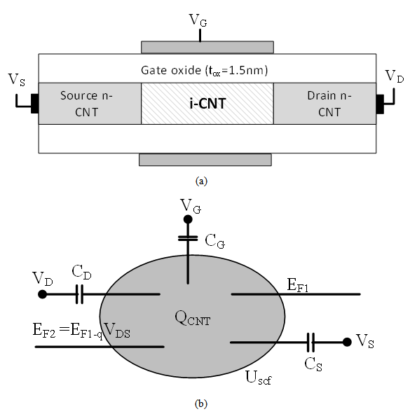 | Figure 1. (a) Cross sectional view of the devices. (b). 2D Capacitor model for ballistic transistors. Top barrier potential controlled by capacitive effect of gate, source and drain potential [7] |
3. Results and Discussions
- This CNTFET configuration considers a (13,0) zigzag CNT with a bandgap ~0.83eV and a diameter ~1.02nm. The oxide thickness is taken as 1.5nm which separates the coaxial gate from the intrinsic part of the nanotube. The simulation is done with a gate and drain control parameters of 0.88 and 0.035. In addition, the source Fermi level was chosen to be -0.32eV. To investigate the influence of the temperature on the attributes of CNTFET, the temperature has been varied from 300K to 500K under different dielectric constant values. Different dielectric constants has been taken for this simulation. To plot the I-V curves, the gate and drain voltages were both been varied from 0 to 0.6V.Figure 2 (a) and (b) illustrates the output characteristics of the predefined structures at the room temperature and extreme condition with different dielectric constants. It can seen that some reported experimental characteristics were compared with the simulation results for d = 1.6 nm, tox = 50 nm, T = 300K, and Ef = −0.05 eV. The experimental data are extracted from fig 2 of ref [11]. There are some variations between experimental and simulated one as the parameters are different. It can be seen that, with increase in temperature, drain current is also increasing with a low gate source voltage. From figure 2(a) it is also evident lower temperature (300K) has a higher drain current than 500K.When the gate voltage is high this condition is valid at low drain voltages, despite of non-ballistic conditions, However, in saturation regime, the higher temperature drain current dominates the lower ones like ballistic region. Figure 2(b) shows comparison of the output characteristics (ID-VDS) of the CNTFET in 300K and 500K with different gate biases with dielectric constant value of 30. The figure depicts that with higher dielectric constant, the drain current at saturation region and at VGS = 0.6V, becomes approximately equal despite of temperature variations. Also the magnitude of the drain current rises high with high dielectric constant value.
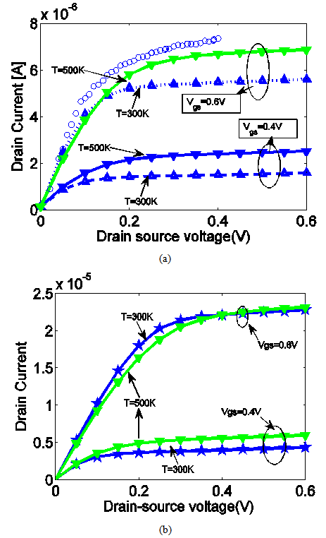 | Figure 2. Comparison of the output characteristics (ID-VDS) of the CNTFET in 300K and 500K with different gate biases. (a) with dielectric constant 3.9 with experimental data (circlet lines ) (b) with dielectric constant 30 |
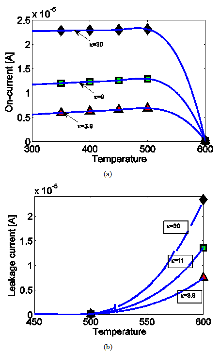 | Figure 3. (a) On-state drain current versus Temperature at VGS=0.6V and VDS=0.6V with different dielectric constants. (b) Leakage current as a function of temperature at at VGS=0V and VDS=0.6V with different dielectric constants |
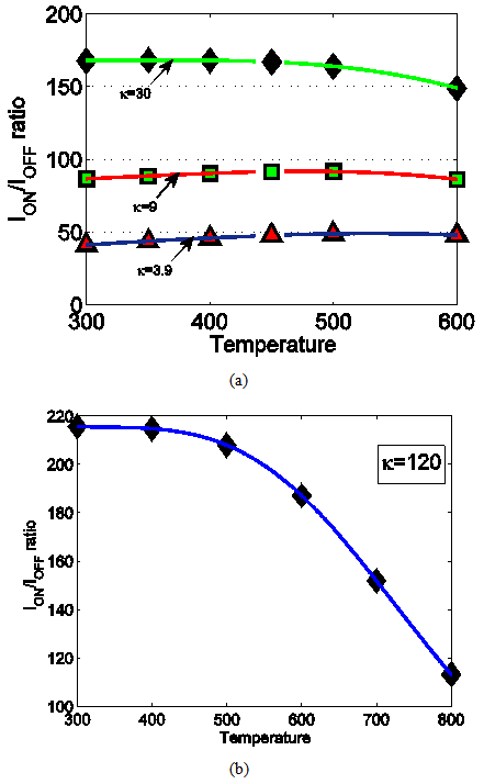 | Figure 4. ION/IOFF current ratio versus Temperature (a) for different dielectric constant (b) for a higher value (κ=120) of dielectric constant |
 | (12) |
 is the charge density and
  is local electrostatic potential. The limit of
  is vital in case of propagation delay parameter where total capacitance is considered [15]. As shown in figure 5, the value of quantum capacitance increases as the temperature increases. Also with a higher value of κ, the value remains small which effects the performance of CNTFET devices in an adverse way. In this simulation gate voltage is taken as 0.3V.
 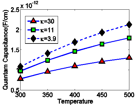 | Figure 5. Quantum Capacitance vs Temperature for different dielectric constants |
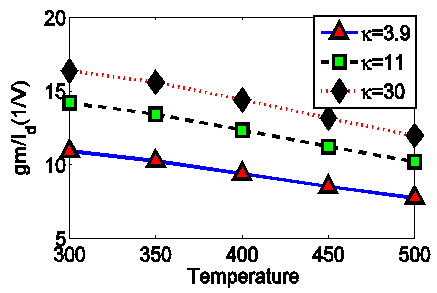 | Figure 6. Variation of gm/Id (/V) ratio vs Temperature with different κ values |
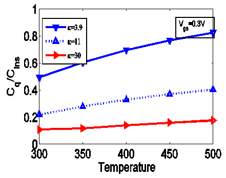 | Figure 7. Capacitance ratio vs Temperature for different dielectric constants |
 | (13) |
 is the permittivity of free space (F/cm2). The small value of the ratio indicates that in deep nanometer regime, quantum capacitance in CNTFET devices decreases. So an ambient temperature as well as optimised choice of dielectric constant value should be chosen for designing a devices. Also a higher quantum capacitance/insulator capacitance can be reached at a gate voltage of 0.3V with higher dielectric constant value. So lower gate voltage shows significant capacitive effect.Figure 6 shows the drain induce barrier effect (DIBL) as a function of temperature. DIBL increases the leakage current with the capability of swinging the channel from off state to conduction state. As a result, it turns the device ON very quickly and hence lowers down the threshold voltage. So the control of the gate voltage over the channel is reduced. Also with higher value of dielectric constants the DIBL remains almost unchanged. Due to all this reasons, the circuit should designed with a reduced DIBL effect. The figure shows that by increasing the temperature the undesirable DIBL increases.
 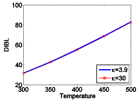 | Figure 8. Drain-induced barrier lowering (DIBL) as a function of temperature with different dielectric constant |
4. Conclusions
- In this paper the attributes of carbon nanotube field-effect transistors (CNTFETs) by varying the temperature with respect to different dielectric constants have been comprehensively investigated under non- ballistic condition. Under higher value of temperature and dielectric constants, current ratio decreases. Also drain current under different temperature with different dielectric constant changes with a less magnitude in non-ballistic condition comparing to the ballistic one. However higher κ value has little impact on the DIBL effect comparing to the temperature effect. So suitable κ with ambient temperature should be chosen for design.
ACKNOWLEDGEMENTS
- The authors are grateful to the Department of Electrical and Electronic Engineering of Ahsanullah University of Science and Technology (AUST) that make this work possible.