B. A. Abdurakhmanov1, M. K. Bakhadirkhanov1, H. M. Iliyev1, S. B. Isamov1, E. B. Saitov1, A. Mavlyanov1, H. U. Kamalov2, Z. Saparniyazova2, O. Sattarov1, U. Kh. Sodikov1, N. F. Zikrillayev1
1Department of Electronics and Microelectronics, Tashkent State Technical University, Tashkent, 100095, Uzbekistan
2Department of Semiconductor Devices, Karakalpak State University, Nukus, Uzbekistan
Correspondence to: B. A. Abdurakhmanov, Department of Electronics and Microelectronics, Tashkent State Technical University, Tashkent, 100095, Uzbekistan.
| Email: |  |
Copyright © 2014 Scientific & Academic Publishing. All Rights Reserved.
Abstract
The paper reports that under certain thermodynamic and doping conditions, the monoatomic and binary clusters of impurity atoms in the silicon lattice are likely to assemble. The effect could help to shape nano-variband structures with controlled band gap.
Keywords:
Single crystalline silicon, Binary clusters, Multiply charged monoatomic clusters, Nano-variband structures
Cite this paper: B. A. Abdurakhmanov, M. K. Bakhadirkhanov, H. M. Iliyev, S. B. Isamov, E. B. Saitov, A. Mavlyanov, H. U. Kamalov, Z. Saparniyazova, O. Sattarov, U. Kh. Sodikov, N. F. Zikrillayev, Silicon with Clusters of Impurity Atoms as a Novel Material for Photovoltaics, Nanoscience and Nanotechnology, Vol. 4 No. 3, 2014, pp. 41-43. doi: 10.5923/j.nn.20140403.01.
1. Introduction
The lower efficiency ratio the conventional solar cells tend to manifest is likely to be a major obstacle preventing widespread use of solar energy around the world. The lower efficiency ratio of solar cells is caused mainly by the inefficiency in the utilization of the entire solar spectrum in the modern solar cells.Therefore, we assume that one could substantially improve the efficiency of modern silicon cells by generating mono-and binary clusters of impurity atoms in the bulk silicon which would create local micro- and nano-scale Schottky barriers as well as hetero-and variband semiconductor structures with controlled band gap covering the entire spectrum of solar radiation, and especially the infrared spectrum. In this paper we propose that one could develop efficient multi-stage solar cells based on silicon with clusters of impurity atoms of varying nature.
2. Main Body
Large-scale application of solar power stations in all areas of human life is mainly determined by their efficiency, reliability and the cost of solar cells. Meanwhile, the efficiency ratio of conventional solar cells based on silicon almost hit the wall, having reached their maximum of ∼ 20%. [1]This is mainly due to the inability to take the advantage of the wider infrared region of the spectrum (λ=1,2÷3 micron) which accounts for nearly ∼40% of solar energy for generation of charge carriers (because of hνg). Ultraviolet and visible spectra of the Sun where hν>Eg due to thermalization of hot carriers generated by the absorption of photons is characterized by the loss of solar energy [2]. The existing technology for manufacturing silicon solar cells is not likely to overcome these losses.The above problem is partially solved by using multi-stage photocells based on compound semiconductors such as GaAs, AlGaAs, ... [3]. However, the technology for manufacturing such solar cells is rather complicated and requires the availability of expensive equipment. Besides that, the cost of such solar cells does not allow their widespread use and the development on their basis of powerful solar plants. Therefore, this problem can be solved successfully either only through the development of novel classes of semiconductor materials or on the basis of novel physical phenomena.In this respect, the monoatomic and binary clusters of impurity atoms in the silicon lattice do represent greater scientific and practical interest, which lets one create nano-variband structures with controlled band gap [4]. The technology of establishing such clusters in the silicon lattice with pre-defined parameters can be successfully implemented on the basis of low-temperature diffusion [5].It was revealed that under certain thermodynamic and doping conditions one could establish nano-scale and microscopic single-atom and binary clusters on the surface and in the bulk crystal alike to a predetermined density. To generate the binary clusters one must take into account the reactivity, solubility, diffusivity and the state of impurity atoms in the lattice. It is also necessary to determine the thermodynamic conditions required for the formation of complexes between these impurities, resulting in the formation of a new elementary lattice from within the silicon lattice. The experimental studies have shown that when it comes to the formation of binary clusters, atoms of group VI elements (S, Se, Te), as well as impurity atoms of fast diffusible impurity atoms of group II elements, as well as the iron group elements tend to be more effective.The choice of Mn was determined by the fact that Mn in the Si lattice produces clusters consisting of four atoms, and can also act as a multiply charged centre and behave as a powerful magnetic cluster. Powerful electric field is generated in the vicinity of such clusters which results in the formation of nano-scale variband local structures [6], wherein the band gap can vary in the range of hν = 0,4 - 1,2 eV. Such structures can eventually absorb energy throughout the entire spectrum of solar radiation.As it was reported in [7, 8], under certain thermodynamic conditions, the manganese atoms and chalcogenide tend to form electrically neutral complexes, Fundamental parameters of such complexes or clusters in the lattice (for example, Eg), differ from the fundamental parameters of Si. The presence of sufficiently high concentration of clusters can significantly extend the spectral sensitivity region.We have conducted doping of silicon with the group VI dopants (S, Se, Te) and manganese both simultaneously and in sequence. As evidenced by the results of studies of electrical, photoelectric and microscopic parameters, and as microprobe studies have shown, that although the impurities of the above elements in silicon behave as donor impurities and create two donor energy levels, on the other hand, electrically neutral molecules are being created between the atoms of the elements of group VI and manganese. The formation of these electrically neutral complexes is basically due to the fact that the elements of the group VI in silicon are located in the crystal lattice site and do represent double donors; manganese in such doping conditions could also be located in lattice site and behave as a double acceptor impurity atom.In this case, the group VI atoms can give away their two extra electrons to the neighboring manganese atom and provide it with full tetrahedral bond. It should be noted that the tetrahedral covalent bond in the lattice is not disrupted in this case and the group VI atoms and manganese produce no energy levels in the forbidden band. As a result, new elementary lattices such as Si2S++Mn--, Si2Se++Mn--, Si2Te++Mn-- form within the silicon lattice (Fig. 1). As the concentration of impurity atoms of group VI and manganese increase, the concentration of such new binary elementary cells rises, thus paving way for the formation of binary clusters (Fig. 2).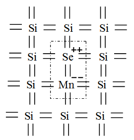 | Figure 1. Formation of new elementary lattice cell of Si2Se++Mn-- |
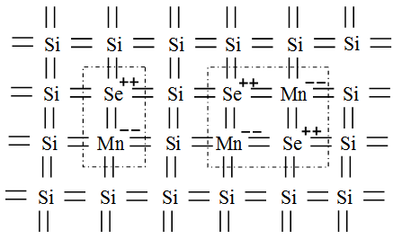 | Figure 2. Formation of binary clusters |
As theoretical calculations and the results of research have shown, the energy required to release an electron in a lattice of Si2S++Mn--, as well as in clusters created on the basis of such elementary lattices, significantly varies from the band gap of Si, i.e. nano-variband structures: “silicon lattice - Si2S++Mn--”, and “silicon lattice - binary clusters” are likely appear. Depending on the nature of such clusters of Si2S++Mn--, Si2Se++Mn--, Si2Te++Mn, one can vary the width of the forbidden band in a wide range toward higher and smaller Eg, alike. Calculations and preliminary results of experiments related to the investigation of photoelectric properties have demonstrated that nano-variband structure based on “binary clusters – Si” may have a width of the forbidden band in the range Eg = 1,6-0,8 eV. As we have shown in [6], nanoscale variband structures of silicon - [(Mn)+8 B-1] +7 are also established in the course of formation of multiply charged clusters of manganese atoms in the lattice of silicon.Having investigated the photoelectric properties of such structures, it was established that in such variband structures, the band-gap varies in the range of Eg = 0,4-1,12 eV, i.e. substantially covering the entire infrared spectrum of solar radiation [6].Thus, in silicon with binary and multiply charged monoatomic clusters one can anticipate the generation of charge carriers not only at hν>Eg,, but also at hνg, thereby significantly expanding the spectral sensitivity region toward higher and smaller wavelengths. The application of such materials in the design and development of solar cells permits to significantly increase their effectiveness by maximizing the use of the IR light from the Sun, as well as minimizing energy loss due to thermalization. The principal task is to control the concentration of clusters so that their contribution is not negligent compare to the intrinsic light in silicon.Calculations suggest that while the concentration of binary and multiply charged clusters in the silicon lattice is in the range of N∼1018 см-3, the efficiency of solar cells can be improved by at least 10%. Fig. 3 shows the spectral sensitivity region of solar cells fabricated using conventional silicon (curve 1) and the Si with multiply charge clusters atoms of Mn (curve 2).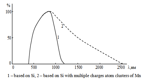 | Figure 3. Spectral area of sensitivity of solar cells |
Curve 2 is simulated based on a study of photoelectric properties, whereby we assume that in such variband structures, the band gap is likely to vary in the range of Eg = 0,4÷1,12 eV, i.e. substantially covering the entire IR-spectrum of solar radiation.In view of the above mentioned, one can state that the main task is to determine the optimal thermodynamic and process conditions to establish maximum concentration of clusters thus enabling to design on their basis more efficient solar cells.Therefore, it can be said that the silicon with mono-and binary clusters might eventually represent a unique material for future photovoltaics as one could develop multi-stage solar cells on the basis if such materials on a single chip without having to use complex manufacturing operations and expensive semiconductor materials such as AIIIBV and AIIB. One could say that such materials represent a virtually novel scientific opportunity in material science, photovoltaics and optoelectronics to name a few.The results of investigations indicate that such ordering of clusters of impurity atoms occurs throughout the entire bulk of the crystal. So far, no physical mechanism is available to explain this phenomenon. However, the process of ordering of clusters leads us to conclude that there is the possibility of diffusion of clusters with relatively higher ration of diffusion. However to prove the above results one needs to carry out detailed thorough research and investigations. It was figured out that as the temperature of additional heat treatment increases the ordering of clusters collapses again and they become evenly distributed again. Preliminary investigations in I-V-curve of cluster – Si by microprobe have shown that such a structure is characterized by almost ideal I-V-curve with very little reverse current and it starts to manifest sensitiveness to irradiation and temperature.
3. Conclusions
Multi-stage silicon photovoltaic cells with clusters of impurity atoms of a varying nature, in contrast to multi-stage photocells based on AIII BVI compounds, require neither complicated manufacturing process nor expensive technological equipment. Besides that, they manifest high efficiency ratios. Since these solar cells are based on silicon, at certain stage it becomes possible to reduce the cost of manufacturing solar cells and launch their mass production.
References
| [1] | Г.Г. Унтила, Т.Н. Кост, А.Б. Чеботарева, М.Б. Закс, А.М. Ситников. |
| [2] | Alan ll., Fahrenbruch, Richard H. Bube/Fundamentals of solar cells/Photovoltaic solar energy conversion/New York, 1998. |
| [3] | Ж.И. Алферов/Избранные труды нанотехнологии/ Москва, 2011/Магистр-Пресс. |
| [4] | З. М. Сапарниязова, М. К. Бахадырханов, О. Э. Саттаров, Х. М. Илиев, К. А. Исмаилов, Н. Норкулов, Д. Ж. Асанов. Взаимодействие многозарядных нанокластеров атомов марганца и серы в кремнии неорганические материалы, 2012, том 48, № 3, с. 1–4. |
| [5] | Абдурахманов Б.А., Бахадырханов М.К., Илиев Х.М., Насриддинов С.С. О диффузии атомов германия в кремнии // ДАН РУз. 2008. № 1. С.18. |
| [6] | М.К. Бахадырханов, С.Б. Исамов, Н.Ф. Зикриллаев. К. Хайдаров. Наноразмерная варизонная структура в кремнии с многозарядными нанокластерами. Микроэлектроника, 2013, том 42, № 6, с. 444–446. |
| [7] | М. К. Бахадырханов, Г. Х. Мавлонов, С. Б. Исамов, Х. М. Илиев, К. С. Аюпов, З. М. Сапарниязова, С. А. Тачилин //Электрофизические свойства кремния, легированного марганцем методом низкотемпературной диффузии// Неорганические материалы, 2011, том 47, № 5, с. 545-550. |
| [8] | M.K. Bakhadirkhanov, Sh. I.Askarov and N. Norkulov// Some features of chemical interaction between fast diffusing impurity and a group VI element in silicon//phys. stat. sol. (a) 142, 339(1994), subject classification: 61,70; S5.11. |


 Abstract
 Reference
 Full-Text PDF
 Full-text HTML