-
Paper Information
- Paper Submission
-
Journal Information
- About This Journal
- Editorial Board
- Current Issue
- Archive
- Author Guidelines
- Contact Us
Nanoscience and Nanotechnology
p-ISSN: 2163-257X e-ISSN: 2163-2588
2014; 4(2): 34-40
doi:10.5923/j.nn.20140402.03
Investigation of CNTFET Performance with Drain Control Coefficient Effect
 Abstract
 Reference
 Full-Text PDF
 Full-text HTML
Sabbir Ahmed Khan1, Nirjhor Tahmidur Rouf2, Mahmudul Hasan3, Sharif Mohammad Mominuzzaman4
1BRACU Robotics, School of Engineering and Computer Science, BRAC University, Dhaka-1212, Bangladesh
2Control and Applications Research Centre, School of Engineering and Computer Science, BRAC University, Dhaka-1212, Bangladesh
3School of Engineering and Computer Science, BRAC University, Dhaka-1212, Bangladesh
4Department of Electrical and Electronic Engineering, Bangladesh University of Engineering and Technology, Dhaka-1000, Bangladesh
Correspondence to: Sabbir Ahmed Khan, BRACU Robotics, School of Engineering and Computer Science, BRAC University, Dhaka-1212, Bangladesh.
| Email: |  |
Copyright © 2014 Scientific & Academic Publishing. All Rights Reserved.
A deep study on the effects of drain control coefficient (αD) on the performance of Carbon Nanotube Field Effect Transistor (CNTFET) has been conducted in this work. In this research, a new analytical CNTFET simulation along with a MATLAB multiple parameter approach model with 3D output has been employed to examine the device performance. It is found that- drain current, drain conductance and transconductance increase with high drain control coefficient causing the device to perform better. However, DIBL also increases with αD resulting in degraded performance of the device. In addition, subthreshold swing moves away from the ideal value as αD goes up which is also not desired for low threshold voltage and low-power operation of scaled down FETs.
Keywords: Drain Control Coefficient (αD), CNTFET, Drain Current, Transconductance
Cite this paper: Sabbir Ahmed Khan, Nirjhor Tahmidur Rouf, Mahmudul Hasan, Sharif Mohammad Mominuzzaman, Investigation of CNTFET Performance with Drain Control Coefficient Effect, Nanoscience and Nanotechnology, Vol. 4 No. 2, 2014, pp. 34-40. doi: 10.5923/j.nn.20140402.03.
Article Outline
1. Introduction
- The existing Silicon technology is struggling to keep up with the demands of Moore’s Law and International Technology Roadmap for Semiconductors (ITRS) [1]. Carbon Nanotube (CNT), since its invention by S. Iijima [2], has aroused the curiosity of researchers from the world over for FET applications because of its excellent mechanical [3] and electrical properties [4], [5]. The performance of CNTFET under different conditions have already been analysed and reported by a number of researchers in recent years [6-18]. Previously, the effect of dielectric constant (K), gate oxide thickness, temperature, chirality and gate control coefficient on the performance of Carbon Nanotube Field Effect Transistor (CNTFET) has been studied by Khan et al. [6-10], [19] with a three dimensional multiple parameter simulation model. It has been found that ION/ IOFF, transconductance and average velocity carrier goes up with high K and so, the on-state current of the CNTFET goes up. At the same time, the subthreshold swing also rises with the rise of the value of K. Scientists have observed that the on current maintains an inverse relationship with the gate oxide thickness [7], [10], [13], [20], [21]. Traditional MOSFET (Metal Oxide Semiconductor Field Effect Transistor) suffers from channel scattering, tunneling and various other problems when the gate oxide thickness enters the nanometer regime [20]. Carbon nanotubes are not plagued by such problems as all chemical bonds are satisfied in a carbon nanotube and thus, there is less oxide to channel interface problem. A multitude of oxide can be placed on the nanotube and thus, many high-k dielectrics can be incorporated into CNTFET to reduce the tunneling current. Also, a higher ION/IOFF has been reported in lower gate thickness than in higher gate thickness [7], [20]. Furthermore, the effect of temperature on the operation of CNTFET has been investigated and it has been concluded that temperature wields a negligible influence on the performance of CNT transistor [8]. Drain control coefficient (αD) is an important parameter while modelling CNTFET and analysing its performance in both ballistic and non-ballistic regime. Hence, it is very crucial to investigate how CNTFET performance depends on αD. This investigation will also help scientist to perform efficient and optimum CNTFET device fabrication. Hence, this paper endeavours to study the impact of Drain Control Coefficient (αD) on the performance of CNTFET. The experiment has been carried out by analysing the change in current-voltage (I-V) characteristics, transconductance, drain conductance, subthreshold swing and drain induced barrier lowering (DIBL) effect with developed multiple simulation method.
2. CNTFET Structure and Simulation Model
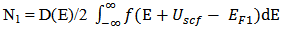
- A MOSFET-like CNTFET has been considered for the purpose of this experiment. The drain and source terminals of the considered FET are heavily doped similar to the conventional MOSFET. This device is designed to overcome the problems faced by SB-CNTFET by operating like a simple MOSFET. The barrier height in this FET is modulated by gate voltage. Charge induced in the channel by the gate terminal controls the drain current [22-24].CNTFET is able to suppress ambipolar conduction. At the same time, it provides longer channel length limit as the density of metal-induced-gap-states are significantly reduced. As the length between gate and source/drain terminals can be separated by the length of source to drain, parasitic capacitance and transistor delay metric can be reduced and hence, operating speed of the device can be increased. It has already been shown [21] that CNTFET provides higher on-current compared to SB-CNFET as its operating principle is similar to that of SB-CNFET with negative Schottky barrier height during on-state condition and so the upper limit of CNTFET performance can be justified.A three dimensional multiple simulation tool [25] was developed based on ballistic nanotransistors theory [22] and FETToy tool [26]. The flow diagram of the simulation model is depicted in APPENDIX [19] and code has been developed using MATLAB program. The detailed simulation process has been discussed in our earlier publication [25]. In this modeling, there are several options for choosing particular parameter to observe the effect of CNTFET output while others set as default value. That is the reason of naming it ‘Multiple simulators’. The total simulation is divided into three parts:A. Command WindowB. Physical Calculation C. Final outputCommand window is subdivided into three segments named: Parameter choosing, Deciding range and finally iteration. ‘Command Window’ is the core part to decide the parameters. This research has considered six parameters to observe the CNTFET attributes. In this fragment, researchers have to decide the logical maximum and minimum value for specific parameters. Consequently, the iteration will start according to the range decided by researcher up to maximum value. In addition, if no other parameters are changed than the simulator will go for default value which is set by us. According to the decided parameter and value, simulator starts physical calculation. It takes each value from the range, calculates nine steps of the physical calculation and repeats same patterns for other values also. It calculates until gaining final result for the final values. Immediately after the entire calculation, it sends values to output window for making 3D output. The analysis starts at the top of the energy barrier since current remains the same throughout the channel and all scattering mechanism is neglected. At any specified drain/gate voltage, the drain current is calculated based on the total charge that occupied first subband in the nanotube. The process is repeated for all drain/gate voltage in the specified range before all the drain current values are plotted within a single graph. The model for ballistic CNFET consists of three capacitors, which represents three transistor terminals on potentials at top of barrier. The mobile charge is determined by the local density of states at top of the barrier, location of source and drain levels, EF1 and EF2, and self-consistent potential at top of the barrier, Uscf. Steps of calculating the drain current [22]:1. Consider a value of Vg, Vds, Vs and EF1. For simplicity, Vs is grounded as potential reference.2. Compute the total charge on nanotube channel. The charge at top of the barrier contributed from source and drain are given as
 | (1) |
 | (2) |
 | (3) |
 | (4) |
 | (5) |
 | (6) |
 | (7) |
 | (8) |
3. Results and Discussions
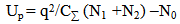
- For the purpose of this research, a (13,0) CNT was considered which had a bandgap of ~0.83 eV and a diameter of ~1.0184 nm. A coaxial gate, separated by a 1.5 nm thick oxide, was placed around the intrinsic part of the nanotube. For this observation, the temperature was kept constant at 300 K and the gate control coefficient (αG) was set at 0.88. In addition, the source Fermi level was -0.32 and the value of dielectric constant was 3.9.Figure 1 shows the I-V characteristics of CNTFET with respect to drain control coefficient. The drain control parameter was varied from 0.025 to 0.225 at an interval of 0.01. From the figure it is evident that the drain current gradually increases with the increase of drain control coefficient and maintains the trend until it reaches 0.225. This substantiates the claim that drain control coefficient and drain current maintains a proportional relationship [27].
 | Figure 1. Current-Voltage output with respect to Drain Control Coefficient |
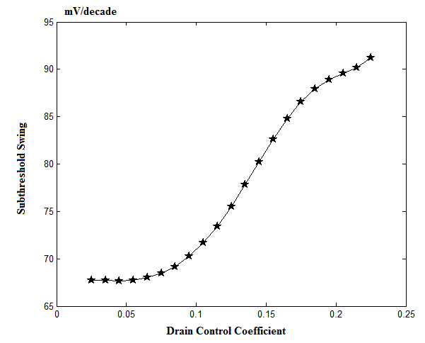 | Figure 2. Subthreshold swing as a function of Gate Control Coefficient |
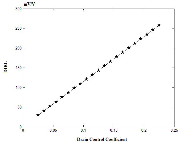 | Figure 3. DIBL effect with Drain Control Coefficient |
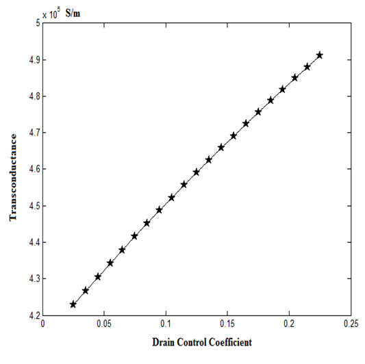 | Figure 4. Transconductance as a function of Gate Control Coefficient |
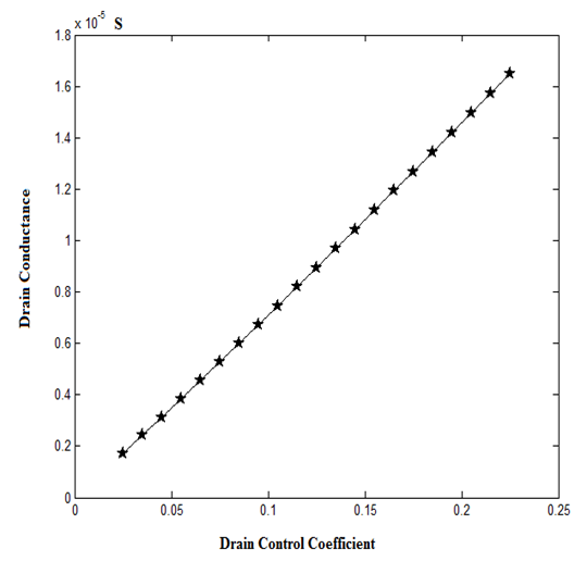 | Figure 5. Drain conductance as a function of Drain Control Coefficient |
4. Conclusions
- In this work, the effect of drain control coefficient on ballistic CNTFET is analyzed with an iterative 3D multiple simulation method. It can be concluded from the results that a high αD causes the device to respond slower. Also, αD increases the leakage current and degrades the CNTFET output. Furthermore, the subthreshold swing moves away from the theoretical value as αD goes higher. However, transconductance and drain conductance increases with drain control coefficient. To sum up, a lower value of drain control coefficient (αD) is more desirable for better CNTFET performance.
ACKNOWLEDGEMENTS
- This research is thankful to BRAC University Robotics research lab and Bangladesh University of Engineering and Technology for their continuous support though out the research. We also want to thank Mr. Md Zahangir Alom, senior lecturer, department of Computer Science and Engineering (CSE), BRAC University for his valuable suggestion while developing MATLAB code.
Nomenclature
Appendix
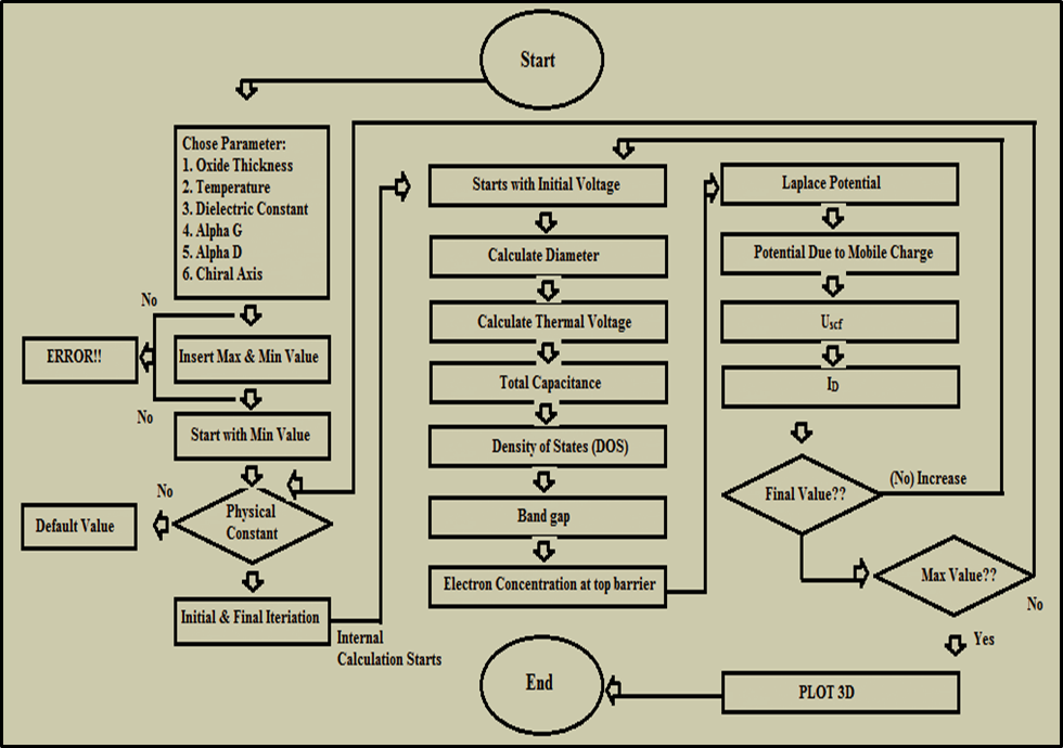 | Flow diagram of the multiple parameter approach simulation tool |