Ilya A. Obukhov
Nanoelectronics TD, Korolev, 141070, Russia
Correspondence to: Ilya A. Obukhov, Nanoelectronics TD, Korolev, 141070, Russia.
| Email: |  |
Copyright © 2012 Scientific & Academic Publishing. All Rights Reserved.
Abstract
Possibility of creation of the planar one-dimensional quantum devices with electric characteristics similar to elements of standard microelectronics are discussed. Such devices may be effectively used in electronic circuits since for there is a big set of well-known circuit design solutions. Functioning of represented devices named Relaxation Quantum Transistor and Quantum Transistor with Injection Gate base on nonequilibrium quantum effects. Modern nanolithography allows to form InSb structures with sizes necessary for obtaining of such effects. Calculations show that for the considered devices: current density ~ 109 – 1011 A/m2, voltage ~ 0,1 V – 1,0 V and limit frequencies ~ 10 THz – 104 THz.
Keywords:
Quantum Wire, InSb, Relaxation Quantum Transistor, Quantum Transistor with Injection Gate
Cite this paper: Ilya A. Obukhov, Planar One-Dimensional Quantum Devices, Nanoscience and Nanotechnology, Vol. 3 No. 5, 2013, pp. 115-122. doi: 10.5923/j.nn.20130305.02.
1. Introduction
The one-dimensional conductor is the object in which the energy spectrum of charge carriers are quantized in two directions and it is continuous in the third direction[1]. In this third direction the charge transport is possible in the one-dimensional conductor.At non-zero temperatures an energy spectrum of electrons may be considered as quantized if the gap between the first and second energy is more than energy of thermal fluctuations kT, where k – is the Boltzmann constant, and T – is the absolute temperature. The elementary estimates show that, this requirement will be executed if, for the linear size of structure in the direction of dimensional quantization, the inequality | (1) |
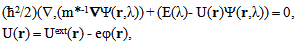
is fair[2]. Here ħ – is the Planck constant and m* - is the electron effective mass. At room temperature (T = 300º K) Ldq equaled approximately 15,1 nm for Si, 25,3 nm for GaAs и 57,9 nm for InSb. Potential reliefs for electrons in a Quantum Wire (QW) are shown in Fig. 1. Here QW is the one-dimensional conductor with square cross-section with the linear size L placed between two contacts. In the field of the sizes L < Ldq the reduction of size L leads to growth of height of a potential barrier to the electrons created by theone-dimensional conductor. As shown in the calculations presented in Fig. 2 at size L reduction twice the current density in a QW decreases more than 3,5 times. This suggests that a conductivity of the one-dimensional conductor playing a role of the conductive channel of a QW decreases by 3,5 times. Thus, the important feature of one-dimensional quantum structures are the strong dependence of their electric characteristics from of the geometrical sizes. This property can be used in the design of the electronic devices based on quantum wires. As shown in works[2,3] by "purely geometrical" methods, it is possible to create elements with demanded electric characteristics. The tool for this purpose is nanolithography.Modern nanolithography allows to controllably form the planar objects with the characteristic sizes less than 30 nanometers[4,5]. It is less than twice the length of dimensional quantization Ldq at room temperature for such material as InSb application of which in nanoelectronics is actively discussed nowadays[6,7,8]. Thin films of InSb on isolating substrates or heterostructures withtwo-dimensional electronic gas on border InSb – AlxIn1-xSb can serve as initial structures for the creation of the planar one-dimensional quantum devices described in this article.The detailed analysis of functioning of these quantum devices was presented in quoted works[2,3,11]. Here the general features of their work are discussed. The multiphase model of charge transport[3,9] was used for simulation of devices characteristics. In this model it is supposed that each state of electron represents the separate phase of electronic gas numbered by index λ and described by the chemical potential F (t,r,λ). In stationary case the equations of model can be written as[2]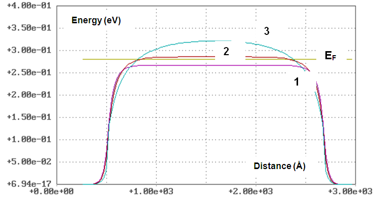 | Figure 1. Potential reliefs for the electrons created by the "volume" semiconductor, (curve 1) and by the one-dimensional conductors from this material of square cross-section section with the linear size L = Ldq, (curve 2) and L = Ldq/2, (curve 3) between metal contacts. Calculations were carried out at a room temperature T = 300°K |
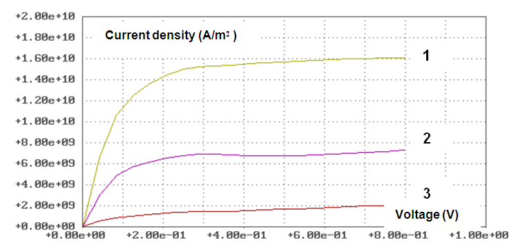 | Figure 2. Current Voltage Characteristics of Quantum Wires with conductive channels in the form of one-dimensional conductors from InSb of square cross-section of the various sizes: 1 – L >> Ldq ("volume" material); 2 – L Ldq; 3 – L Ldq/2. Calculations were carried out at a room temperature of T = 300°K |

 | (2) |
where Ψ(r,λ) – is the electron wave function in λ-state; E(λ) – is the electron energy in λ-state; Uext(r) - is the built-in potential caused, for example, by the breaks of band gaps of heterostructures; e - is the charge of electron; φ(t,r) - is the self-consistent electric potential; ε – is dielectric permittivity; Гλλ’ and Гλ’λ are the probabilities of electrons transitions between λ and λ’-states; n(r,λ) and n(r,λ) – are the electron concentration and the density of electron flow calculated by formulas 
 | (3) |
where τ(λ) – is momentum relaxation time. Boundary conditions for the wave function and the electrostatic potential in different cases are well known[1,2]. For the chemical potentials in contacts of devices we required 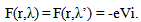 | (4) |
Here Vi – is voltage on contact with number i. Equality of chemical potentials with different λ means the local chemical equilibrium between λ-phases of electron gas.
2. Relaxation Quantum Transistor
In the article[3] the quantum device with electric characteristics similar of usual bipolar transistor was offered. This device was named the Relaxation Quantum Transistor (RQT). There is a real possibility of creation of RQT based on InSb now. It was caused by achievements of nanolithography.The topology of RQT demonstrated in Fig. 3. The potential relief for electrons under condition of zero voltage on contacts is shown in Fig. 4. The area of the device which, by analogy to the bipolar transistor was named, the Base represents the "thin" one-dimensional conductive channel located between two "wide" one-dimensional conductive channels which were named the Emitter and the Collector. According to Fig. 4, the area of Base represents a potential barrier for electrons.Within a multiphase model of charge transport[3,9] the theoretical analysis of functioning of RQT is carried out in works[2,3]. It was supposed that electronic gas consists of three phases corresponding to electrons getting to the device from collector, emitter and base contacts. The current flow through the structure shown in Fig. 4, creates the nonequilibrium electrons in areas of junctions between conductive various cross-section channels. The current density of the nonequilibrium electrons not linearly depends from the voltage at the base contact. As a result RQT can function as the amplifier of the electric signal submitted between base contact and the emitter contact.The electric characteristics of RQT based on InSb one-dimensional conductive channels are presented in Fig. 5 and 6. They are similar to the corresponding characteristics of the ordinary bipolar transistor.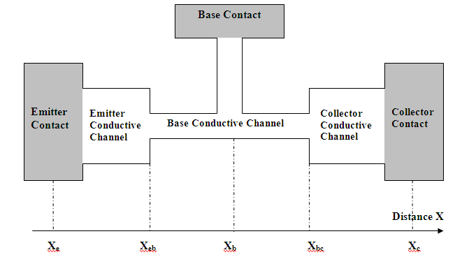 | Figure 3. Topology of Relaxation Quantum Transistor |
 | Figure 4. Potential relief for electrons in RQT in direction from Emitter to Collector under conditions Ve = Vb = Vc =0 V. Cross-sections sizes of Emitter’s and Collector’s Conductive Channels equal Lqd and cross-section size of Base’s Conductive Channel equals Lqd/2 |
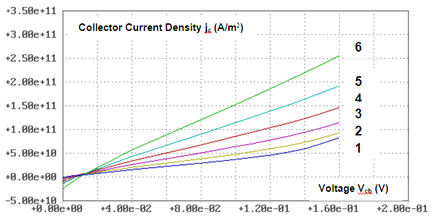
 | Figure 5. Current Voltage Characteristics of RQT in circuit with common base when: 1 – Veb = 0,01 V; 2 – Veb = 0,025 V; 3- Veb = 0,03 V; 4 – Veb = 0,05 V. Calculations were carried out at room temperature T = 300° K |
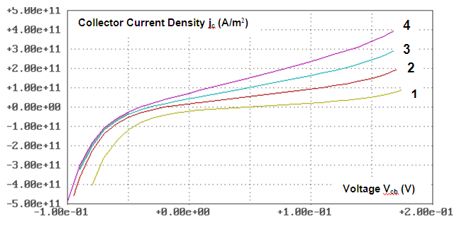
 | Figure 6. Current Voltage Characteristics of RQT in circuit with common emitter when: 1 – Vbe = 0,00 В; 2 – Vbe = 0,01 V; 3- Vbe = 0,02 V; 4 – Vbe = 0,03 V; 5 - Vbe = 0,04 V; 6 - Vbe = 0,05 V. Calculations were carried out at room temperature T = 300° K |
Definition of the factor of amplifying the current for transistor in circuit with common emitter β is given by a ratio | (5) |
Where Jc и Jb – is the current of collector and current of base;  | (6) |
- is factor of amplifying for transistor in circuit with common base; Je – is current of emitter connected with currents Jc and Jb by conservation law | (7) |
As demonstrated in book[2] for factor α the simple estimation is true  | (8) |
Here α0 – is some dimensionless value that depends from topology and regime of functioning of RQT; | (9) |
- is the length of the base conductive channel (correspond to Fig. 3);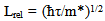 | (10) |
- is the length of relaxation of the nonequilibrium electrons to the state of thermodynamics equilibrium. From ratios (5) and (8) we will find  | (11) |
From formulas (8) and (11) follows that RQT will effectively function as the transistor if estimates are fair  | (12) |
From a physical point of view, it means that the nonequilibrium electrons injected from the emitter to the base at flight to a collector shouldn't have sufficient time for relaxation to a state of thermodynamic equilibrium.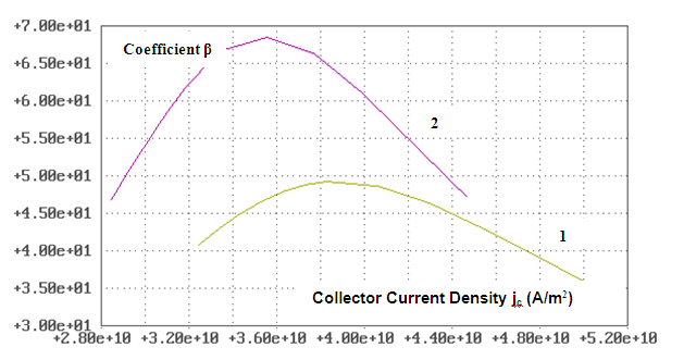 | Figure 7. Coefficient of amplifying of current for transistor in circuit with common emitter β for RQT based on InSb one-dimensional conductive channels when Lb = 80 nm and 1 - Vce = 0,06 V; 2 - Vce = 0,07 V. Calculations were carried out at room temperature T = 300° K |
As for momentum relaxation time τ, using values of this parameter in bulk material at room temperature, it is possible to receive the following estimate for Lrel: 10,0 nanometers for Si; 23,8 nanometers for GaAs and 72,7 nanometers for InSb. The sizes Lrel are close to the corresponding values for length of dimensional quantization Ldq calculated at room temperature. It isn't surprising as the formula (1) can be presented in a form similar to expression (10) 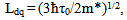 | (13) |
where | (14) |
and the estimation is fair τ ~ τ0.From the given estimates follows that quantum and nonequilibrium effects in solid-state electronic devices show at the same characteristic sizes. If the technology allows to form one-dimensional quantum structures, the same technology allows to create the devices functioning on the basis of nonequilibrium quantum effects.Curves of coefficient of amplifying β for RQT based on InSb at various operating modes at room temperature are presented in Fig. 7. For the calculations Lb was chosen one order with Lrel. Quite acceptable values of β were received. According to formula (11) a reduction in the length of base will lead to increase of coefficient of amplifying of transistor β.
3. Quantum Transistor with Injection Gate
Field-Effect Transistors (FET) of different types are usually used as basic elements of digital circuits. However, in one-dimensional electronics there are problems connected with a low transconductance of such devices. Even at very high specific transconductance about 109 А/Vm2 the absolute transconductance appears not above 106 – 105 A/V[8,10]. It is caused by the fact that current of the device decreases proportionally to cross-section area of a conductive channel. The prize in the specific transconductance, obtained by use of the quantum, effects considerably increasing sensitivity of the device to voltage on the gate, is insufficient for compensation of small cross-section area of a conductive channel of Quantum Field Effect Transistor (QFET).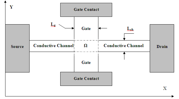 | Figure 8. Topology of Quantum Transistor with Injection Gate |
As a solution of the specified problem the Quantum Transistor with Injection Gate (QTIG) was offered in article[11]. The principle of work of this device is based on non-equilibrium electronic phenomena. The device represents two perpendicular quantum wires with the conductive channels of various cross-section as shown in Fig. 8. Thicker one-dimensional conductor plays a role of an injection gate, and the thinner one-dimensional conductor plays a role of the conductive channel of the device.Potential profiles for electrons in quantum wires, composing QTIG, are represented in the Fig. 9-10. Calculations were carried out for InSb quantum wires with Lch = 3Ldq/4, Lg = 2Ldq at room temperature T = 300° K and under condition of zero voltage on all contacts. It was supposed that one-dimensional conductors from InSb have square cross-section. Modeling of charge transport in the QTIG was based on the equations (2) in which electronic gas consisted of two phases: electrons in the conductive channel and electrons in the gate.At the chosen parameters the area of crossing of one-dimensional conductors Ω appears a potential hole for the electrons reaching the device from a source and a drain, and a potential barrier to the electrons getting to the device from contacts to a gate.At current flow between source and drain, the injection of electrons to conductive channel from a potential hole in area Ω, may be realized. The mechanism of such injection is completely similar to the injection mechanism from contact to conductive channel of quantum wire[2]. The intensity of injection can be regulated by the voltage on the gate.In Fig. 11 the top curve and the bottom curve are the Current Voltage Characteristics (CVC) of quantum wires from which QTIG consist. The middle curve in Fig. 11 is CVC of conductive channel of QTIG under condition of zero voltage on the gate. Comparison of the bottom and middle curves shows that the injection of electrons from a gate increases a current in the channel by several times.Injection of electrons in QTIG occurs by transitions of electrons from energy states, in a quantum hole, to states with energy more than the height of potential barriers in the conductive channel with quasi-impulse shift by ± π/2These transitions are caused by the stochastic scattering of the electrons on phonons, impurities and the at each other. The family of QTIG current voltage characteristics for different voltage on the gate is represented in Fig. 12. The considered device is the two-port network. However, in calculations it was assumed that both gate contacts were under identical voltage Vg. In such regime QTIG is functionally similar to the field effect transistor but the characteristics of QTIG are better than characteristics of QFET. In particular, for a transconductance the estimation is fair gm ∂Id/∂Vg ∼ 103 A/V. 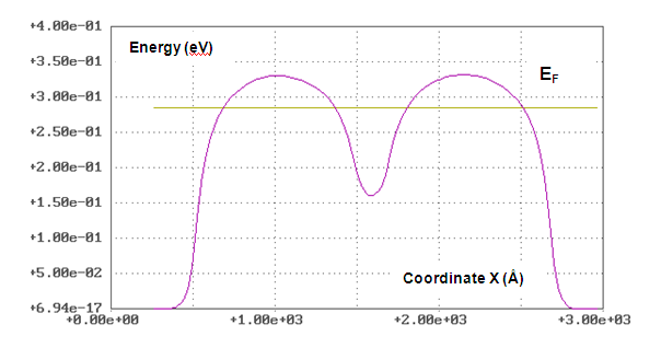 | Figure 9. Shows the potential relief for electrons in conductive channel of QTIG under a condition of zero voltage on all contacts. Calculations were carried out for InSb quantum wires with Lch = 3Ldq/4, Lg = 2Ldq at room temperature T = 300° K |
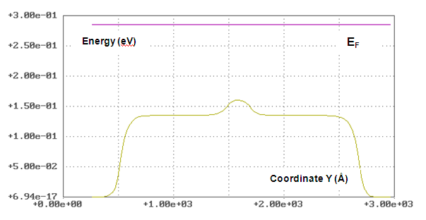 | Figure 10. Potential profile of electrons in InSb gate quantum wire of QTIG at zero voltage on all contacts. Calculations were carried out for InSb quantum wires with Lch = 3Ldq/4, Lg = 2Ldq at room temperature T = 300° K |
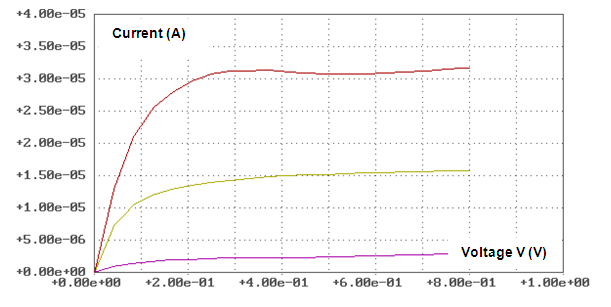 | Figure 11. Bottom curve is CVC of quantum wire with cross-size L = 3Ldq/4; top curve is CVC of quantum wire with cross-size L = 2Ldq; middle curve is CVC of conductive channel of QTIG under conditions Vg Vs = 0 V, V = Vd Vs; T = 300° K |
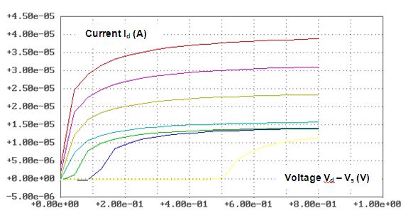 | Figure 12. Drain current of QTIG for different voltage on the gate (curves are highlighted from the bottom upwards): Vg Vs= 0,50 V, 0,10 V, 0,03 V, 0,00 V, 0,01 V, 0,02 V, 0,03 V |
It is 103 times higher than for QFET. And it testifies to efficiency of drain current control at use of an injection gate in the form of a quantum wire with higher concentration of charge carriers (in comparison with a conductive channel).The injection of electrons is a nonequilibrium process, localized in an area with a specific size order Lrel. If the length Lg is considerably greater than length of relaxation Lrel of nonequilibrium electrons, the injection will be carried out in boundary areas of Ω only. In this case the structure shown in Fig. 8 will not function as the transistor. It will turn into two quantum wires with widths equal to Lch and with one general contact the role of which will be played by a gate.
4. Conclusions
The presented research shows that planar one-dimensional quantum devices are perspective for the application in nanoelectronics. Relaxation Quantum Transistor and Quantum Transistor with Injection Gate should have the characteristics similar to characteristics of traditional devices of microelectronics. The creation of such an element base of nanoelectronics will allow to use the circuit design solutions that were created over the previous years of microelectronics development. Calculations show that in devices based on one-dimensional conductors very high density of currents about 109 – 1011 A/m2 and rather high currents from 0,1 µA to 10 µA may be reached. Thus the specific bias voltage is small, they are about 0,1 V – 1,0 V. This suggests the low power consumption from 105μW to 1,0 μW.The specific resistance sizes are fair 103 Ohm – 107 Ohm. Specific capacity of active areas of devices are about 10-3 F/m2. The simple calculations allow to estimate limit frequencies for the considered devices flim ~ 10 THz – 104 THz.Sizes of active areas of offered devices should provide the dimensional quantization of electrons energy. The length of dimensional quantization essentially depend on a used material and temperature. At a room temperature of (Т = 300°К) for InSb this equals 57,9 nm.Essentially important influence for the output characteristics of one-dimensional quantum devices render the nonequilibrium effects caused by charge transport. Purposeful use of these effects at design stage allows to achieve demanded functional properties and high controllability of quantum devices. For practical use of nonequilibrium effects, it is necessary to be able to create planar objects with the controllable sizes smaller than the lengths of relaxation of nonequilibrium electrons Lrel. For InSb at room temperature this length equates 72,7 nm. Modern nanolithography allows to form structures with the sizes of about 30 nm. It is quite sufficient for creation of the planar one-dimensional quantum devices based on InSb described in this article. Thus, the modern nanotechnology allows for us today to create the electronic devices which can provide for electronic circuits with integration degree of 1010 elements on a square centimeter, Terahertz frequencies of functioning and the low level of power consumption.
References
| [1] | Datta S., Electronic Transport in Mesoscopic Systems. Cambridge University Press, UK, 1997. |
| [2] | Obukhov I.A., Nonequilibrium effects in electronic devices, Veber (Moscow – Kiev – Minsk – Sevastopol), Russia, 2010. |
| [3] | Obukhov I.A., “About the possibility of relaxation quantum devices creation”, Tech. Phys. Lett., v. 19, no 9, pp. 537-538, 1993. |
| [4] | Landis S., Nano-lithography. London, UK : ISTE ; Hoboken, NJ : Wiley, 2011. |
| [5] | Seisyan R.P., “Nanolithography in Microelectronics”, J. Tech. Phys., v. 81, no. 8, pp. 1-14, 2011. |
| [6] | Ashley T., Barnes A.R., Buckle L., Datta S., Dean A.B., Emeny T.M., Fearn M., Hayes D.G., Hilton K.P., Jefferies R., Martin T., Nash K.J., Phillips T.J., Tang W.H.A. and Chau R., “InSb-based Quantum Well Transistors for High Speed, Low Power Applications, Proceedings of 7th International Conference: Solid-State and Integrated Circuits Technology”, v. 3, pp. 2253–2256, 2004. |
| [7] | Datta S., “The 21st Century Energy Efficient Logic Transistor”, http://www.sematech.org/meetings/archives/litho /8065/pres/ Key%20Note%20Suman%20Datta.pdf |
| [8] | Das Suprem R., Delker Collin J., Zakharov Dmitri, Chen Yong P., Sands Timothy D. and Janes David B., “Room temperature device performance of electrodeposited InSb nanowire field effect transistors”, Appl. Phys. Lett., v. 98, 243504 (3 pages), 2011. |
| [9] | Obukhov I.A., “About the Frequency-Dependence of Electrical Characteristics of Quantum Devices”, Nanoscience and Nanotechnology, v.2, no.5, pp. 144 - 147, 2012. |
| [10] | Martel R., Shcmidt T., Shea H.R., Avouris P., “Single- and multi- wall carbon nanotube field effect transistors”, Appl. Phys. Lett., v. 73, no17, pp. 2447 - 2449, 1998. |
| [11] | Obukhov I.A., Kvjatkevich I.I., Lavrenchuk A.A., Rumjancev S.V., “Static Characteristics of Crossed Quantum Wires”, in Proceeding of 14th International Crimean Conference Microwave & Telecommunication technology, pp. 507 – 511, Sevastopol, Ukraine, 2004. |
 Abstract
 Reference
 Full-Text PDF
 Full-text HTML