F. Iqbal, S. Naseem, S. Riaz, A. Sadiqa, Shahzad Naseem
Centre in Excellence for Solid State Physics, University of The Punjab, Quaid-e-Azam Campus, Lahore
Correspondence to: F. Iqbal, Centre in Excellence for Solid State Physics, University of The Punjab, Quaid-e-Azam Campus, Lahore.
| Email: |  |
Copyright © 2012 Scientific & Academic Publishing. All Rights Reserved.
Abstract
Carbon nanostructures growth is described on the surface of stainless steel SS201 using chemical vapor deposition technique at reaction temperature of 800℃. The metal surface serves as catalyst and support the growth of nanostructure. Substrate was prepared for nanostructure growth by different treatments involves cutting, polishing, cleaning and etching. Scanning electron microscope was used as characterization technique of nanostructures. Variety of carbon nanostructures i.e. nanowires, nanograins, nanotubes, nanorice, nanowalls, nanobelts were observed with different diameter range. The nanostructure mostly found was the Y-shaped nanowires with approximately 50nm diameter. It was observed that nanogrowth vary on different areas of the same substrate. This variation of growth was correlated with Difference in the cone angle of deposition, Difference in the working distance, Difference in the gas composition, Presence of thermal zone in the furnace.
Keywords:
Carbon Nanostructures, SEM, Stainless steel, Carbon Nanowires, CNTs
Cite this paper: F. Iqbal, S. Naseem, S. Riaz, A. Sadiqa, Shahzad Naseem, A Study of Deposition, Characterization and Growth Conditions of Carbon Nanostructures on Stainless Steel (201), Nanoscience and Nanotechnology, Vol. 3 No. 4, 2013, pp. 96-103. doi: 10.5923/j.nn.20130304.03.
1. Introduction
The device miniaturization is a challenging drift in the present and future device techniques ranging from customers products to the biomedical applications[1]. It is very interesting that different carbon nanostructures such as fullerenes, nanotubes, nanocones and graphene have different mechanical and physical behaviors[2]. In nanotechnology, there are various classifications of nanostructures. Nanostructures are normally differentiated on the basis on geometrical properties. Different types of nanostructures by their geometrical structures includes nanocages, nanocrystallites, nanobelts, nanoneedles, nanocomposites, nanofabrics, nanofibers, nanoflakes, nanoflowers, nanofoams, nanomeshes, nanoparticles, nanopillars, nanopin films, nanorings, nanorods, nanoshells, nanopowders, nanoclusters, nanowires, nanotubes, quantum dots, quantum heterostructures[3,4]. It is also important that there are rich numbers of new phenomena associated with nanometer sized structures. The most outstanding conventional examples include size- dependent excitation or discharge[5], quantized (or ballistic) conductance[6], Coulomb blockade[7], and metal insulator transition[8]. It is established that quantum detention of electrons by the potential wells in carbon nanostructures can make available one of the most powerful resources to manage the electrical, optical, magnetic, and thermoelectric properties of a solid-state efficient materials.
2. Experimental Techniques
Stainless steel 201(5x5 mm) was used for the carbon nanostructure synthesization which provides catalytic sites for nanostructures directly on substrates[9] without any catalyst source[10]. The preparation of the substrate includes mechanical and electrochemical polishing in order to remove contaminants and stains on the surface. Subsequent etching with HCl solution insures the availability of the deposition sites[11,12]. Following by a rinse with distilled water, the substrates were prebaked at 850℃ in N2 atmosphere for 30 min[13]. The surface treatment can be described[10]. Ambios-XP1 surface profilometer and Leica DM4000M Optical Microscope was used for the examination of the every step during preparation.For nanostructures growth substrates were put onto the heating block of the TCVD reactor. After attaining the desired temperature, methane (CH4) was fed into the reactor to start the synthesis of carbon nanostructures. Methane (CH4) gas was used with the pressure of 0.75torr which decomposed to provide carbon in the presence of arc discharge produced (shown in the figure) by applying the high voltage of 30KV. Carbon was deposited at reaction temperature of 850℃ for 20 minutes.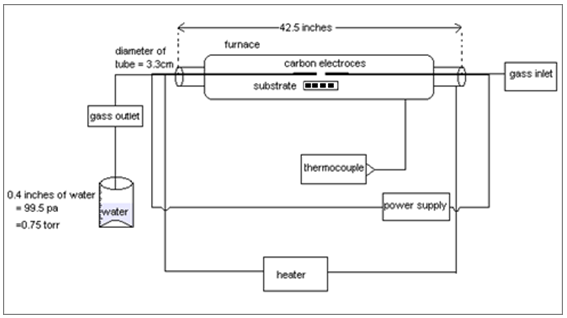 | Figure 1. Schematic diagram of homemade furnace used for Thermal CVD |
Surface profilometery of SS201:BEFORE POLISHING: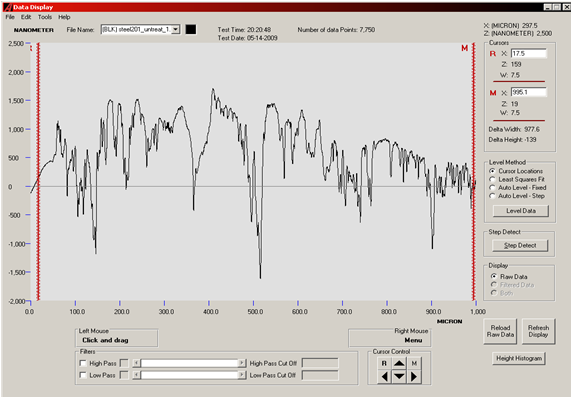 | Figure 2. Surface profilometery result of SS201 showing the roughness of substrate |
ATER POLISHING: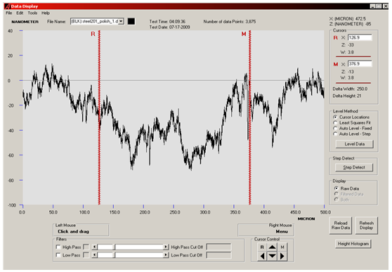 | Figure 3. Surface profilometery result of SS201 showing the smoothness of substrate after polishing |
AFTER ETCHING: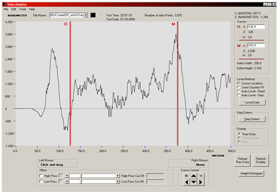 | Figure 4. Surface profilometery result of SS201 showing the etched surface of substrate after polishing |
The surfaces of substrates were very rough as shown in optical micrographs. We wished too see surfaces critically, all depths and sharp peaks present there. So, surface profilometer model XP1 was used to measure the roughness and waviness of substrates. Substrates were then polished in order to get planer surfaces. There are several reasons to get a substrate with a good optical finish. In the present work it was necessary to avoid cumbersome purification steps and to get carbon nanostructures. Three substrates were prepared in this way. Then substrates were etched with HCl acid to enhance the growth process. Roughness of the SS201 before and after polishing and then after etching is given in table.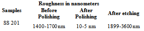 Carbon nanostructures were examined with Hittachi Scanning Electron micrographs.Nanostructures deposited on etched portion of SS201:
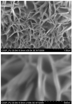
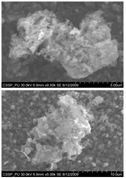
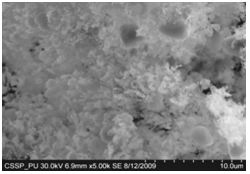
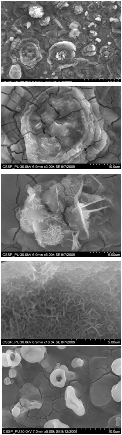 | Figure 5. SEM image showing deposition of combined flower like structure of different nano growth on the etched portion (A) All Regions of nanostructures (B) One of the region indicating deposition of bundles of nanowires (C) indicates the deposition of nanowalls (D) deposition of bundles of nanowires on another portion of figure ‘A’ (E) deposition of diskettes over large area |
 | Figure 6. SEM image of (A) densely and uniformly distributed nanowires (B) magnified image of nanowires |
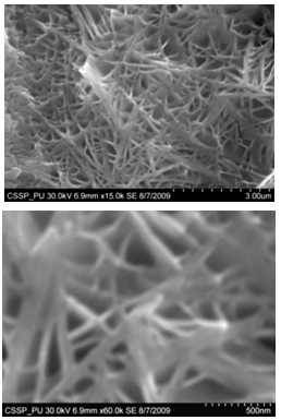
 | Figure 7. (A) (B) &(C) Magnified SEM images of nanowalls |
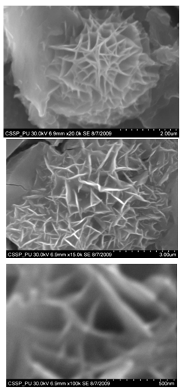
 | Figure 8. SEM image of (A) doublets Y-shaped nanowires uniformly and densely distributed (B) magnified image of doublets Y-shaped nanowires |
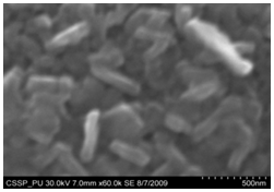 | Figure 9. Magnified SEM image of nanorice |
 | Figure 10. SEM image of (A) nanorice distributed on the boundary of etched grain (B) magnified image of these nanorice |
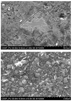
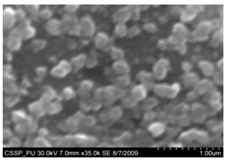 | Figure 11. Magnified SEM image connected nanograins |
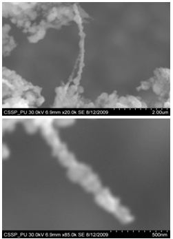
Nanostructures deposited on Unetched portion of SS201: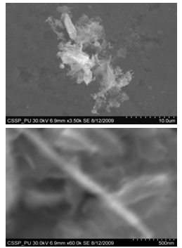 | Figure 12. SEM image of (A) connected Y-shaped nanowire on a cluster of amorphous carbon (B) magnified image of Y-shaped nanowire |
 | Figure 13. Magnified SEM image of (A & B) each of amorphous carbon clusters |
Figure 5 (A) shows the deposition combined flower like structure of different nano growth on the etched portion of the SS201. Each of the region of 5(A) is then magnified to show these deposited structures. One of the region indicated is magnified and shown in figure 5 (B). In this region bundles of nanowires in flower are deposited. These nanowires are uniformly and densely distributed within that area and shown in figure 6 (A) (B). One of another region deposited by nanowalls is magnified in figure 5 (C). Figure 5 (D) indicate the deposition of bundle of nanowires on some other portion of the etched substrate. On the right side of substrate diskettes are deposited, which are distributed on a large area. These diskettes are of different sizes and shown in figure 5 (E)[14].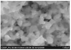 | Figure 14. Magnified SEM image showing amorphous carbon cluster |
 | Figure 15. SEM image of (A) suspended and connected Y-shaped nanowire starting from one cluster and ending at the other end of the same cluster (B) nanowire with amorphous carbon deposited at one end of cluster |
 | Figure 16. SEM image of Sun flower like structure |
Figure 7 (A) shows the two locations of deposited nanowalls from figure 5 (C). These two regions are further magnified and shown in figures 7 (A) (B). In these figures nanowalls of specific height, width and length can clearly be seen. These nanowalls are magnified up to 100,000 times and shown in figure 7 (C). Nanowalls are very clear even at this huge magnification. Carbon-nanowalls (CNWs) can be thought as two-dimensional graphite nanostructures having edges comprised of stacks of plane graphene sheets which are standing almost vertically on the substrate. These sheets form a high aspect ratio wall structure. The thickness of CNWs ranges from a few nm to a few tens of nm[15]. Nanowalls have potential practical application in batteries, catalysts, light emission/detection, gas sensors, field emission and biomedical devices. It is found that the threshold field emission field of carbon nanowalls is much lower than that of carbon nanotubes, which makes them capable for field emission displays and other miniaturized electron sources. The nanowalls exhibit extremely different surface morphology as compared to fullerenes and carbon nanotubes, in particular their two-dimensionality and their high surface area. So far the focus is on the latter aspect and developing a templating method to fabricate a class of nanostructured materials based on the novel surface morphology of the carbon nanowalls. Exploration of application in other fields is under way[16, 17].Figure 8(A) shows the magnified image of deposited nanowires which are densly and uniformly distributed within the area. This region is further magnified and shown in figures 8(B). These all nanowires are of Y-shape and all are doublets. Even at 100,000 time magnification these doublets can clearly be seen as in figure 8 (B). Figure 9 indicates the deposition of nano rice on one of the regions in etched portion of SS201. These nano rice ranges from 50-60 nm. Figure 10(A) also shows the deposition of nanorice on etched portion. These nanorice are distributed on the boundary of etched grain on the substrate. These nanorice are magnified and shown in figure 10(B). The diameter of these nanowires ranges from 40-50nm. Connected nano grains of diameter 100-150 nm are also deposited on the etched portion of SS201as shown in figure 11. The connected behavior of these nanograins shows that they can also make a proper structure after having favourable conditions. Figure 12(A) (B) shows the growth of connected Y-shaped nanowire on a cluster of amorphous carbon in the unetched portion of the SS201. This nanowire is started from the cluster and ended at the same cluster forming a Y. the diameter of this wire is approximately 50nm. In figure 13 (A) and 13(B) two amorphous carbon clusters are shown. The amorphous carbon is deposited from the thermal decomposition (pyrolysis) of carbon feedstock gas[18].Figure 14 also shows the magnified image of deposition of amorphous carbon cluster. Growth of suspended and connected Y-shaped nanowire is also observed on the unetched portion of this substrate. This Y-shaped nanowire is started from one cluster and ended at the other end of the cluster as shown in figure 15(A). Figure 15(B) indicates the growth of nanowire coming out from same carbon cluster with amorphous carbon deposited on it. The overgrowth contained graphitic sections and had no well defined structure. The overgrowth increases the surface area making the nanowire more appropriate for use as electrodes[19]. Sun flower like structure is also deposited on the unetched portion of the substrate a shown in figure 16. The growth is not complete here. At many areas of this region the central portion of the sun flower is complete but the outer portion is not complete. Distance of all substrates was different horizontally and vertically from the center of electrodes. The temperature was also different for all substrates. Cone angle varies for all substrates and for single substrate as well. The gas velocity through the reaction tube is not even and although the flow over the majority of the substrate could be expected to be roughly constant at millimeter scale, not for nanometer scale. There will be regions of slow moving gas near the furnace tube wall. There, therefore exists a concentration gradient across the width of the each substrate due to differential gas velocity. Growth rate also varies at each point on the substrate because all the decomposed carbon will not deposit exactly below on the substrate but some of the decomposed carbon atoms will move forward due to gas flow onto the next substrate. All substrates are half etched and half unetched. Due to different compositions in all substrates etching rate is different hence forming valleys of different composition. These all variations will leads to deposition of different carbon nanostructures on all substrates. Best results of carbon nanostructures are achieved on SS201 where the cone angle ranges from 45o to 60 o and temperature was 800℃. SS201 contains Cr=16.0-18.0%, Ni=3.50-5.50%, Mn=5.50-7.50% and iron 67.51%.
References
| [1] | Y. Li: A Novel Statistical Methodology for Sub-100 nm MOS-FET Fabrication Optimization and Sensitivity Analysis, 2005, Int. Conf. Solid State Devices and Materials, 622-623. |
| [2] | C. Stampfer: Electromechanical transducers based on soingle-walled carbon nanotubes, 2007, Ph.D dissertation, ETH Zurich. |
| [3] | U. Müller: Nanostructures in Inorganic Structural Chemistry, 2007, 2nd edn,John Wiley & Sons, 241–245. |
| [4] | M. Köhler, W. Fritzsche: Characterization of nanostructures in Nanotechnology, 2008, 2nd edn, Wiley-VCH,Weinheim, 211–224. |
| [5] | C. B. Murray, C. R. Kagan, M. G. Bawendi: Synthesis and characterization of monodisperse nanocrystals andclose-packed nanocrystals assemblies, 2000, Annu. Rev. Mater. Sci., 30, 545. |
| [6] | G. Grabecki: Ballastic transport phenomena in nanostructures, 2007, Act. Phys. Pol. A., 112, 127. |
| [7] | K. K. Likharev, T. Claeson: Single Electronics, 1992, Sci. Am., 20, 80. |
| [8] | G. Markovich, C. P. Collier, S. E. Henrichs, F. Remacle, R. D. Levine, J. R. Heath: Architectonic Quantum dots solid, Acc. Chem. Res., 1999 32, 415. |
| [9] | T. Hiraoka, T. Yamada, K. Hata, D. N. Futaba, H. Kurachi, S. Uemura, M. Yumura, S. Iijima: Synthesis of Single- and Double-Walled Carbon Nanotube Forests on Conducting Metal Foils, J. Am. Chem. Soc., 2006, 128, 13338–13339. |
| [10] | C. Masarapu and B. Wei: Superhydrophobic conductive nanotubes coatings for steel, Langmuir., 2007, 23, 9046. |
| [11] | D. Park, Y. H. Kim, J. K. Lee: A novel ion exchange process for As removal, J. Materials Sci., 2003, 38, 4934. |
| [12] | Y. H. Tang, Y. F. Zheng, C. S. Lee, N. Wang, S. T. Lee, T. K. Sham: Carbon mono-oxide assisted growth of carbon nanotubes, Chem. Phys. Lett., (2001), 342, 259-264. |
| [13] | Y. Yun, R. Gollapudi, V. Shanov, M. Schulz, Z. Dong, A. Jazieh: Carbon nanotubes grown on stainless steel to form plate and probe electrodes for chemical/biological sensing, J. Nanosci Nanotechnol., 2007, 7, 891. |
| [14] | P. J. F. Harris: Carbon Nanotubes and Related Structure, Illustrated, Cambridge University Press, 2001. |
| [15] | M. Hiramatsu, M. Hori: Carbon Nanowalls (Synthesis and emerging applications), 1st Edition, Springer, 2010. |
| [16] | W. Yihong, B. J. Yang, H. Sun, Y. P. Feng: Carbon nanowalls and related materials, J. Mat. Chem., 2004, 9, 469-477. |
| [17] | J. Song, M. Sun, Q. Chen, J. Wang, G. Zhang, Z. Xue, J. Appl. Phys 37 (2004) 5 |
| [18] | K. B. K. Teo, C. Singh, M. Chhowalla, W. I. Milne, Encyclopedia of Nanosience and Nanotechnology X (2003) 13 |
| [19] | J. Song, M. Sun, Q. Chen, J. Wang, G. Zhang, Z. Xue, J. Appl. Phys 37 (2004) 5 |
 Abstract
 Reference
 Full-Text PDF
 Full-text HTML