O. V. Naumova, Yu. V. Nastaushev, T. A. Gavrilova, F. N. Dultsev, L. V. Sokolov, A. L. Aseev
A.V. Rzhanov Institute of Semiconductor Physics, Russian Academy of Sciences, Siberian Branch, Lavrent’ev Avenue, 13, Novosibirsk, 630090, Russia
Correspondence to: Yu. V. Nastaushev, A.V. Rzhanov Institute of Semiconductor Physics, Russian Academy of Sciences, Siberian Branch, Lavrent’ev Avenue, 13, Novosibirsk, 630090, Russia.
| Email: |  |
Copyright © 2012 Scientific & Academic Publishing. All Rights Reserved.
Abstract
Chemical and electrical passivation of Si nanowhiskers (NW) by means of plasma chemical oxidation and nitridation of Ti nanolayers evaporated onto MBE-grown Si NW were used. Influence of formed Ti nanolayers on the properties of Si NWs were evaluated by means of scanning electron microscopy, and current-voltage and current-temperature measurements. Specific aspects addressed in the present study were modification of the morphology and electrical properties of Si NWs after plasma chemical treatments of samples resulting in the formation of TiOx or TiONx layers on the NWs surface. It is shown that at temperatures close to room temperature the conductivity of NWs, as well as that of the silicon substrate on which the NWs were grown, was defined by centers with ionization energies (0.20-0.22) eV. Depending on particular conditions, the plasma treatments used to form the TiOx or TiONx layers on the NW surface brought about the following phenomena: (i) introduction of centers with ionization energies 0.12 eV and (0.03-0.04) eV that defined the conduction of Si NWs at temperatures below 160 K and (ii) change of shape of the NWs (from cylindrical to conical) that may prove useful for optical applications of Si NWs. On the basis of NW arrays, surround-gate field-effect transistors (FETs) with SiO2/TiONx composite dielectric were fabricated. The threshold-voltage value of the FETs, Vth=0.3 V, and the dielectric constant of the TiONx layers ε=14.7 at frequency 100 kHz were evaluated.
Keywords:
Nanowires, Surface Characterization, Surface Treatments
Cite this paper: O. V. Naumova, Yu. V. Nastaushev, T. A. Gavrilova, F. N. Dultsev, L. V. Sokolov, A. L. Aseev, Properties of Si Nanowhiskers Coated by TiOx and TiONx Layers, Nanoscience and Nanotechnology, Vol. 3 No. 1, 2013, pp. 14-18. doi: 10.5923/j.nn.20130301.03.
1. Introduction
Silicon whiskers, or vertical nanowires, are promising structures due to their potential use in novel nanoelectronic, photonic and photovoltaic devices. In particular, epitaxially grown Si NWs are good candidates for post-CMOS logical elements due to their potential compatibility with the well-established CMOS technology[1-3]. The growth of vertical nanowires and the technology of high-k dielectrics make it possible to obtain vertical surround-gate field-effect transistors (FETs) with better electrostatic gate control of the conducting channel than in conventional planar architectures. Another very important aspect in using such FETs is fabrication of 3D silicon nanosensors[4, 5]. Reproducibility of structural and electrical properties of NWs is the key prerequisite for their application in various nanodevices. That is why methods of chemical and electrical passivation of nanowhiskers compatible with the methods of application of dielectric coatings on the NW surface were the subject of many previous studies. It is this matter that was also addressed in the present study. Application of a dielectric coating onto the surface of Si is a method traditionally used for stabilizing the Si surface in Si-based technology. Growth of a thermal silicon dioxide layer still remains a preferable strategy here since the density of states at the Si/dielectric surface can be made low. The composite dielectrics formed on the base of the SiO2 and TiO2 layers (with high dielectric constant) are well known as an alternative ultrathin gate dielectrics for memory and logic devices. The TiO2 films are prepared by various techniques (chemical vapor deposition, pulse laser deposition, spattering, sol-gel techniques[6-9]) that requires relatively high temperatures. Yet, the process of NW growth is based on using, as a catalyst, metal drops, which, as a rule, lead to degradation of NW characteristics under high-temperature conditions because of introduction of deep levels into Si. That is why a low-temperature process for application of passivating coatings onto NW surface is required. In the present study, we propose using, as a coating for Si NWs, a composite dielectric formed by a chemically grown SiO2 layer and a TiOx or TiONx layer obtained by treating Ti nanolayers in plasma[10]. The tasks in the present work were as follows: (i) examination of the influence of plasmochemical treatments of Ti on the structural and electrical properties of Si NWs, (ii) characterization of the Si/composite dielectric system, and (iii) investigation into possibilities of forming test and device structures based on NWs coated with the proposed composite dielectric (with the example of surround-gate FETs).
2. Experimental
Si nanowhiskers were grown by molecular-beam epitaxy on (111)-oriented phosphorus-doped (5 Ω∙cm) Si wafers using Au as a catalyst for NW growth. A detailed description of the NW growth procedure was given elsewhere[11]. The passivation of Si nanowhiskers was implemented as follows. First, the native-oxide layer was removed from the NW surface to chemically grow a SiO2 layer on this surface by treating the samples in boiling nitric acid. Then, 5-13 nm thick Ti metal layers were deposited in high vacuum, 10-5 – 10-7 Pa, onto the grown SiO2 layer using the e-beam sputtering technique (ANGARA setup). The rate of deposition of the metal layer was 10 nm/min. Finally, treatments in O2 or N2 plasma at radiofrequency 13.56 MHz (“MATRIX”) were used to obtain respectively a TiOx or TiONx nanolayer[10]. The coatings used and the conditions under which the coatings were formed are indicated in Table 1.| Table 1. Regimes of plasma treatments of the Ti films and the types of formed coatings |
| | No. | Covering | Plasma | RF power, W | t, min | Pressure,Torr | | 1 | TiONx | Nitrogen | 100 | 16 | 0.2 | | 2 | TiOx-1 | Oxygen | 70 | 5 | 0.6 | | 3 | TiOx-2 | Oxygen | 200 | 10 | 0.6 |
|
|
On the basis of Si NWs coated with TiONx layers, surround-gate FETs were fabricated, which were provided with a common contact G to the FET array formed by about one hundred NWs. After the formation of dielectric coatings and the fabrication of FETs, no anneals traditionally used for removal of plasma-induced damages were given to the obtained structures.Scanning electron microscopy (SEM) and current-voltage (I-V) and current-temperature (I-T) measurements were used to characterize the formed NW structures.In the electrical measurements, the Si substrate was used as one of the contacts to the NWs. The other contact to the top ends of Si NWs was formed by vacuum evaporation of an Al layer onto a 400-nm thick polymer sublayer (for more details of the contact formation process, see[12]). The polymer sublayer was used to prevent formation of a short circuit between the top Al layer and the Si substrate. Figure 1a shows a schematic of the test structure. A similar method for forming polymer layers was used in fabricating surround-gate NW FETs. A schematic of an NW FET is shown in Figure 1b. The width of the Al gate in the FET was 300 nm.A drain-current (Ids) versus gate-voltage (Vg) curves of the NW FETs were measured. From those curves, the subthreshold slope S and the threshold voltage Vth of the transistors could be determined. The FET threshold voltage was evaluated using linear approximation of the function Ids/(gm)1/2 (gm is transconductance, gm=dIds/dVg) with subsequent determination of the cutoff at the Vg-axis; in this way, the contribution of the parasitic series resistance induced by the contacts to the structure could be excluded.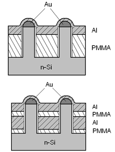 | Figure 1. Schematic of the examined NW structure and surround-gate NW FET |
In addition, CV measurements were made at frequency 100 kHz. From measured maximum capacity, or dielectric capacity Cd, we could determine the dielectric constant εeff of the composite dielectric, whereas from the hysteresis voltage V we were able to evaluate the density of interfacial states at the Si/composite dielectric interface: | (1) |
Where, q is the electron charge.With known value of εeff, resulting from the stack of two dielectric layers, TiONx and SiO2, as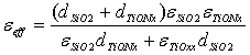 | (2) |
for the layer thicknesses dSiO2=2 nm and dTiONx=13 nm and for εSiO2=3.9, the dielectric constant of the TiONx layer could be calculated. Thicknesses of the SiO2 and TiONx layers were determined using transmission electron microscopy (TEM) technique.As the metal contact to the composite dielectric in the CV measurements, a mercury probe with area 4.26х10-4 cm2 was used.
3. Results and Discussion
Figure 2 shows SEM images of Si NWs after plasma treatments held in regimes 1-3 (see Table 1). Treatments 1 and 2 are seen to be non-destructive ones for NWs, whereas plasma treatments in oxygen held at relatively high discharge powers were found to lead to formation of conical NWs. 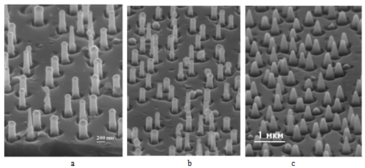 | Figure 2. SEM images of Si nanowhiskers coated with TiONx, TiOx-1, and TiOx-2 layers (a, b, and c, respectively) |
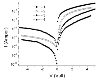 | Figure 3. Current-voltage curves measured at room temperature for structures NW/TiONx (1), Me/Si-Sub (2), NW/TiOx-1 (3), and NW/TiOx-2 (4) |
Figure 3 shows typical current-voltage curves of nanowhiskers measured at room temperature. For comparison, the same figure shows an I-V curve measured on the Me/Si-Sub structure (from which Si NWs were etched out in nitrohydrochloric acid). The rectifying properties of the NW structures were due to the Schottky barrier formed between the metal contact on the top of Si NWs and the n-type conductivity NWs[12].The forward currents (at V=5 V) flowing through the NW structures with Si NWs coated with various coatings are shown in Figure 4. It should be mentioned here that similar measurements were also performed at other voltages, namely, at V=1, 2, 3, and 4 V. The general behavior of the I-T curves was retained, with the current values varying in proportion to V, which observation was indicative of an ohmic conduction through the NW structures. It is seen from Figure 4 that the curves for all measured structures exhibit an exponential dependence of the electric current on temperature, I~exp(-Ea/kT), where Еа is the activation energy for conduction. The values of Ea calculated from the slope of the ln(I)-T curves are summarized in Table 2.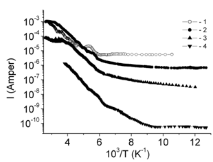 | Figure 4. Current-vs-temperature curves measured at bias voltage V=–5 V on Me/Si samples with etched-out NWs (curve 1) and on samples with Si NWs covered with TiONx, TiOx-1, and TiOx -2 layers (curves 2, 3, and 4, respectively) |
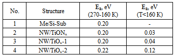
Table 2. Activation energies of the electric current in the various structures
 |
| |
|
It is seen from Table 2 that in the temperature interval (270-160) K the current activation energy in all the structures have close values, about (0.20-0.22) eV. In the temperature interval (160-80) K the current in the Me/Si-Sub structures is almost independent of temperature, whereas the energies Еа in the structures NW/TiONx and NWs/TiOx-1 have close values of (0.03-0.04) eV. In NW structures with TiOx-2 layer the values of Еа proved to be higher, amounting to 120 meV. A comparison between the SEM data of Figure 2 and the results of electrical measurements (Figure 3 and Table 2) leads us to a conclusion that the conductivity of the NW/Ti structures at temperatures (160-300) K after treatments 1-3 (see Table 1) is defined by the same electrically active centers that define the conductivity of the Si substrate on which the NWs were grown. Treatments 1 and 2 are non-destructive treatments; yet, they additionally introduce electrically active centers with low ionization energies (0.03-0.04) eV into Si. Those centers are responsible for the conduction in NWs at temperatures below 160 K. The close values of Ea in the structures treated under different plasma conditions (treatments 1 and 2) allow us to arrive at a conclusion that the nature of the introduced centers does not depend on the plasma composition, being related, most probably, with plasma-induced radiation damages of NWs. Treatment 3 in oxygen plasma (as compared to treatment 2) results in NW destruction and introduction of defects with a higher ionization energy, 0.12 eV, these defects being responsible for the conduction in NWs at temperatures below 160 K.Figure 5 shows the Ids-Vg curves of surround-gate NW FETs measured on a structure with an NW array (see Figure 1b). The composite gate dielectric here was formed by a chemically grown 2-nm thick SiO2 layer and an 8-nm thick TiONx layer. The threshold voltage of the FETs determined from the Ids-Vg curves equals Vth= 0.31 V, and the subthreshold slope is S=140 mV/dec. The relatively high value of S, 140 mV/dec (in comparison with the ideal value 60 mV/dec), can be attributed to the presence of structurally imperfect NWs in the NW array (see Figure 2 a) and/or to scattering of charge carriers on interface states at the dielectric/NW interface. Note that, following the plasmochemical treatment, here again the NW FETs were given no additional anneal.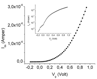 | Figure 5. The curve of Ids vs Vg for an array of about one hundred NW FETs whose surround gate was formed by the nitrided 8-nm thick Ti layer. Vds=0.1 V |
Figure 6 shows the CV curves for an MIS structure with 2-nm SiO2/13-nm TiONx composite dielectric measured at frequency 100 kHz.The dielectric constants of the composite dielectric and the layer calculated from the maximum capacitance by expression (2) on the assumption that εSiO2=3.9 were evaluated to equal εeff=10.7 and εTiONx=14.7, respectively. The hysteresis value ΔV≈1 V translates in a density of surface states Nit~4x1012 cm-2.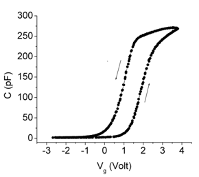 | Figure 6. CV curves of an MIS structure with 2-nm SiO2/13-nm TiONx composite dielectric measured at frequency 100 kHz |
4. Conclusions
It was shown in the present study that the formation process for composite dielectrics based on chemically grown SiO2 layers and TiOx or TiONx layers obtained by treating Ti layers in plasma can be successfully used in fabricating both test and device NW-based structures for electrical characterization of Si nanowhiskers. The use of such dielectrics allows one to obtain reproducible conditions on the surface of Si NWs. It is shown that at temperatures 160-300 K the conduction of NWs covered by the composite dielectric is defined by the same centers that define the conductivity of the Si substrate on which the NWs were grown. Specific features of plasma treatments are: (i) introduction of centers with low ionization energies, (0.03-0.04) eV and 0.12 eV, into NWs, which are responsible for NW conductivity value at temperatures below 160 K, (ii) the possibility to obtain conical NWs (depending on the plasma composition and regime). The latter may prove useful for optical applications of Si NWs. It is shown that the density of states at the interface between the silicon and the composite dielectric formed by a chemically grown SiO2 layer and a nitrided Ti layer initially (in unannealed structures) amounts to ~4x1012 cm-2.
ACKNOWLEDGEMENTS
Work was partly supported by RFBR under Project No. 10-02-00926 and “Growth mechanisms and characteristics of Si and SiGe nanowhiskers” according to basic research RAS Presidium Program N 27.
References
| [1] | T. Bryllert, L.-E. Wernersson, T. Lowgren and L. Samuelson, Nanotechnology, 17, S227 (2006) |
| [2] | O. Hayden, R. Agarwal and W. Lu, Nano Today, 3, 12 (2008) |
| [3] | D. Shir , B. Z. Liu, A. M. Mohammad, K. K. Lew , S. E. Mohney, J. Vac. Sci. & Techn. B., 24, 1333 (2006) |
| [4] | C. Thelander, P. Agarwal, S. Brongersma, J. Eymery, L.F. Feiner, A. Forchel, M. Scheffler, W. Riess, B.J. Ohlsson, U. Gosele, L. Samuelson. Materials Today, 9, 28 (2006) |
| [5] | F. Patolsky, C. M. Lieber, Materials Today, 8, 20 (2005) |
| [6] | G. D. Wilk, M. Wallace, J. M. Anthony, Appl. Phys. Lett., 79, 5245 (2001) |
| [7] | M. Mosaddeq-ur-Rahman, G. Yu, T. Soga, T. Jimbo, H. Ebisu, M. Umeno, J. Appl. Phys., 88, 4634 (2000) |
| [8] | Z. Wang, U. Helmersson, P-O Kall, Thin Solid Films, 405, 50 (2002) |
| [9] | K. Matsuo, K. Nakajima, S. Omoto, S. Nakamura, A. Yagishita, G. Minamihaba, H. Yano, K. Suguro, Japanese Journal of Applied Physics, 39, 5794 (2000) |
| [10] | F. N. Dultsev, S. N. Svitasheva, Yu. V. Nastaushev, A. L. Aseev, Thin Solid Films, 519, 6344 (2011) |
| [11] | L. Schubert, P. Werner, N. D. Zakharov, G. Gerth, F. M. Kolb, L. Long and U. Gösele, Appl. Phys. Lett., 84, 4968 (2004) |
| [12] | O. V. Naumova, Yu. V. Nastaushev, S. N. Svitasheva, L. V. Sokolov, N. D. Zakharov, P. Werner, T. A. Gavrilova, F. N. Dultsev and A. L. Aseev, Nanotechnology, 19, 225708 (2008) |
 Abstract
 Reference
 Full-Text PDF
 Full-text HTML