Bassam G. Rasheed, Mohammed A. Ibrahem
University of Technology, Baghdad, IRAQ
Correspondence to: Bassam G. Rasheed, University of Technology, Baghdad, IRAQ.
| Email: |  |
Copyright © 2012 Scientific & Academic Publishing. All Rights Reserved.
Abstract
Inexpensive silicon solar cell utilizes nanotechnology offers great possibility to enhance the conversion efficiency and reduce the maintenance requirements as well. Moreover, the large surface area of the nanostructured solar cell enables this cell to reduce the number of the required cells. The surface of ordinary solar cell has been reconstructed by electrochemical etching in suitable cell. It is found that the etching time and current density have optimum values to obtain higher conversion efficiency. Effects of these two parameters on the optoelectronic properties of the solar cell have been studied. Spectroscopic methods involving Raman and photoluminescence emission were carried out on the reconstructed surface of the solar cell.Fitting of Raman line shape with theoretical quantum confinement model implies that nanostructure of mean value of 6 nm was established. While the surface morphology investigation reveal synthesize of a pore-like structure separated by thin walls consisting silicon nanostructures.
Keywords:
Silicon Nanostructure, Nanostructured Solar Cell, Etching Process
Cite this paper:
Bassam G. Rasheed, Mohammed A. Ibrahem, "Surface Reconstruction of Electrochemically Etched Nano-structured Solar Cell", Nanoscience and Nanotechnology, Vol. 2 No. 6, 2012, pp. 178-183. doi: 10.5923/j.nn.20120206.05.
1. Introduction
The potential need of the solar cell has been stimulated a great interest last decade. The silicon solar cells are almost rule the photovoltaic solar cell market. The major barrier for the large scale use of solar energy is the high cost and inadequate efficiencies of existing solar cells[1]. Crystalline silicon is unsuitable for use in optoelectronic applications due to its non-radiative phenomena which prevent radiative recombination process. Silicon is a ubiquitous electronic material and the discovery of strong room temperature luminescence from porous silicon in 1990 raised hopes; it may find a new lease of life in the emerging field of optoelectronics[2]. The conventional solar cells used today based on single crystalline silicon has a limited efficiency. Tunableband gap semiconductors have demonstrated extraordinary optical and electronic properties that open up possibilities for revolutionary advances in photovoltaic devices. Currently, the main approach is to produce high efficiency solar cell since the efficiencies of these cells do not exceed 20%. It is very important to innovate a method to harvest incident solar photons with a greater efficiency and economic viability[3].The surface texturing at the top surface of the solar cell could adjust the optical, electrical and consequently the conversion efficiency of the cell. The large surface area of the porous layer helps sun light trapping and omits the expensive antireflection coating. Moreover, the tunable morphology of this layer make it particularly well suited to the photovoltaic applications. Nanotechnology has many potential advantages which open the door to the production of cheaper and slightly more efficient solar cell[4,5]. The reason for potential increase in efficiency using nanostructured solar cell is that absorption of photons is very high due to the carrier density obtained by quantum confinement effects.High efficiency silicon solar cells need textured front surface in nanoscale to reduce reflectance since optical losses due to reflectance of incident solar radiation are one of the most important factors limiting their efficiency[6]. The possible way to overcome the reflectance losses and increasing the surface area of the solar cell is texturing the solar surface. This could be done by various techniques. The most popular technique is the electrochemical etching. Moreover, high quality laser beams make it possible to use laser technology for texturing which is impossible to carry out with any different techniques 7].While one of the promising methods to construct nanostructure morphology is the photoelectrochemical etching[8 – 11]. The optoelectronic properties of the three ordinary solar cells could be used to calculate the conversion efficiencies. The performance of the solar cell could be determined by measuring the conversion efficiency (η), fill factor (F.F) and the open circuit voltage (VOC) as well as the short circuit current (ISC) under illumination of the standard AM1.5 (100 mW/cm2). The fill factor is calculated using the relation | (1) |
Where Pmax= Im X VmWhile the cell efficiency η is given by:η= Pmax / PAM | (2) |
where PAM1.5 = 100 mW/cm2Spectroscopic methods such as Raman scattering and the photoluminescence emission are considered as a powerful nondestructive tools to investigate and characterize nanostructured surfaces / particles.Raman spectroscopy is one of the most suitable methods for investigating and characterizing silicon nanostructures[12,13]. The Raman scattering effect from silicon nanostructured surfaces could be significantly used to determine the nanostructure features when the Raman scattering model incorporates the phonon quantum confinement effect within nanostructures[14]. Therefore, detailed study of Raman scattering line including the line broadening and asymmetry is carried out in this project to determine silicon nanostructures sizes.Theoretical model involves the phonon quantum confinement model was adopted to fit the experimentally obtained Raman scattering lines. This model is given by the relation[13]: | (3) |
Where (ω) is the phonon wavenumber, Γ is the line width, (a) is the silicon lattice constant and (L) is the size in nanometer.Analysis of Raman line depends on the line broadening, asymmetry and size distribution provide significant details about the solar cell surface.The most important advantage of using nanostructured silicon solar cells is its band gap which behaves as a direct band gap semiconductor with large quantum efficiency and may be adjusted for optimum sunlight absorption. This device is interesting because of the possibility for developing a low-cost and high efficiency solar cells operate at the room temperature[14,15]. Aim of this work is to produce textured surface and increase the sun light absorption and subsequently, enhance the solar cell efficiency.
2. Experimental Work
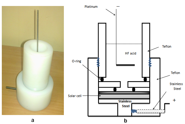 | Figure (1). The fabricated and designed etching cell (a) Photograph and (b) Schematic diagram |
Ordinary p-n silicon of 300 µm thickness solar cell has been used as a starting material to prepare nanostructured solar cell. Surface texturing of this solar cell is accomplished by electrochemical etching and silicon dissolution in HF acid. The etching cell made from Teflon has been designed and fabricated as shown in figure (1) to synthesize nanostructured layer at the top of the solar cell. This design allows using the cell for electrochemical etching. Etching only one side of the solar cell has been considered in this design, while the backside of the solar cell is completely separated from the etching acid, thereby, the metallization of the backside which is coated by aluminum will be protected. Moreover, in order to achieve a homogenous and uniform porous structure layer, an ohmic contact is required on the entire backside surface of the cell. The area of the solar surface that could be etched in this design is 4.5 cm2. The main challenge in this work is to adopt the etching process on the solar cell surface without affecting the underlying junction characteristics. Effect of current density and etching timewere examined. Different current densities and etching time in the range 5- 20 mA/cm2 and 5-20 minutes, respectively were used for the electrochemical etching and to study effect of one parameter, the other was kept constant.Diluted HF acid of 10% concentration was used to initiate a chemical reaction between the florin ions and silicon. The solar cell conversion efficiency is obtained through out calculation of the optoelectronic properties of the nanostructured solar cell. While spectroscopic studies using Raman and photoluminescence emission were employed to characterize the nanostructured surface of the solar cell. Morphological investigations of the nanostructured solar cell werecarried out using SPM and SEM.
3. Results and Discussions
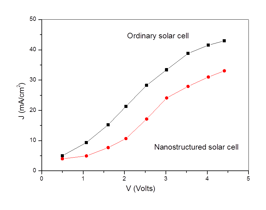 | Figure (2). The J-V behavior to the ordinary and nanostructured solar cell |
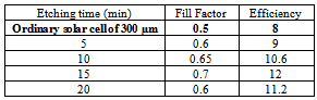
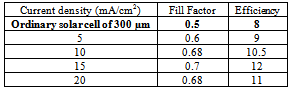
The quantum confinement in nanocrystalline silicon form a hetero-junction structurewhere the porous layer has a much wider energy gap than the crystalline silicon and hence the PS/c-Si may be considered as a hetero-junction between two semiconductors with different forbidden gaps.This leads to increase the resistivity as compared with ordinary solar cell.Increases the volume to surface area of the nanostructured solar cell leads to increasing the light absorption which overcomes the increasing in the surface resistivity and leads to establish efficient coupling.Figure (2)shows a comparison between J-V behaviorofordinaryand nanostructured solar cell.Effects of the etching time and current density on the optoelectronic properties of the nanostructured solar cell were studied. The etching time was varied in the range (5 to 20 minutes) for current density of 15 mA/cm2 and HF concentration of 10%. Figure (3) represents the optoelectronic properties for the nanostructured solar cell. As the etching time proceeds, a remarkable increase in the solar cell efficiency and reaches it optimum value of (12) at 15 minutes and then starts to decrease, as given in tables 1. This could be attributed to the consumption of the all accumulated holes on the surface at this optimum value and farther increase in the etching time causes removal of smaller nanocrystallite sizes and forms a newlayer of larger sizes. Moreover, the current density plays a significant role on controlling the porous layer features which are considered a very important in the solar cell applications. The optoelectronic characteristics of the solar cell of 300 µm for fixed etching time of 10 minutes, HF concentration of 10 % and various current densities ( 5, 10, 15 and 20 mA/cm2) are shown in figure (4). It is found that there is an optimum value of 15 mA/cm2 which gives higher conversion efficiency as given in table 2. The current density is responsible on holes accumulation at the surface. Farther increase of current densities leads to accumulate holes in much higher speed compared with holes consumption speed and then decreases the porous layer thickness. This optimum value for the current density could correlates to the etching time and the HF concentration. 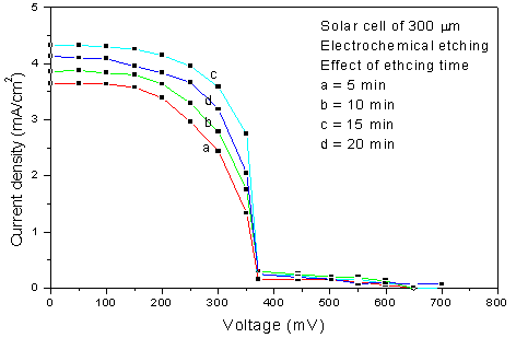 | Figure (3). The optoelectronic characteristic of the 300 µm solar cell prepared by electrochemical etching with different etching times using the optimum current density of 15mA/cm2 at 10% HF concentration |
Table 1. Characteristics of the 300 µm solar cell prepared by electrochemical etchingas a function of etching time
 |
| |
|
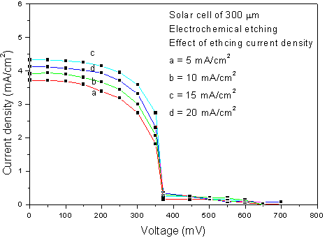 | Figure (4). The optoelectronic properties of the electrochemically etched 300 µm solar cell under different current densities for a fixed time of 10 minutes and 10% HF concentration |
Table 2. Characteristics of the 300 µm thick solar cell etched electrochemically under different current densities
 |
| |
|
The theoretical fitting of the experimentally obtained Raman scattering line reveal existence of silicon nanoparticles of few nanometer in size at the top of the silicon nanostructured solar cell. The Raman line shape is strongly depends on the nanocrystallite size of the solar cell surface due to the effect of the phonon wave function[5]. Size reduction of silicon nanocystallite leads to enlarge the phonon wave function and ultimately, introduce extra width accompanied by increasing the asymmetry of the Raman line. The experimentally observed Raman line for the 300 µm solar cell reveals that the line broadening was 8 cm-1while the asymmetry ratio was 1.5 as shown in figure (5) and the mean nanostructure size is (6 nm) as given in table 3. 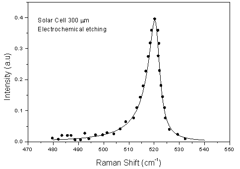 | Figure (5). The Raman line shape of the 300 µm solar cell surface etched electrochemically under15 mA/cm2, 15 minutes etching time and 10% HF concentration |
| Table 3. The experimentally obtained and the theoretical fitting data |
| | Raman line broadening (cm-1) | Raman line asymmetry | The estimated size(nm) | | 8 | 1.5 | 6 |
|
|
The quantum confinement model interprets the recombination process and photoluminescence in silicon nanostructures in room temperature[6]. This model suggests that each nanoparticles constituting the porous layer network gives a sharp peak in the photoluminescence spectrum and different silicon nanoparticles produce a broad emission peak as shown in figure (6). The photoluminescence emission spectra reveal formation of nanostructures on the top surface of the solar cells. 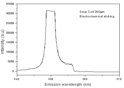 | Figure (6). The photoluminescence emission of the 300 µm nanostructured solar cell prepared by electrochemical etching under10 minutes etching time,10% HF concentration |
It is found that there is a strong correlation between the two spectroscopic methods (Raman and photoluminescence). Both methods indicate abundance of silicon nanostructures at the top of the nanostructured solar cell.The surface morphology of the porous layer examined by SEM and SPM has extremely rich details with respect of range of variation in the pore size, shape and their distribution. The SEM image in figure (7) shows that pore-like structure is formed by the electrochemical etching techniqueunder 15 mA/cm2 current density, 15 minutes etching time and 10 % HF concentration. The layer thickness of this structure was very thin and could be attributed to the effect of the supplied holes to the surface. Holes which are required at the solar surface to initiate the chemical reaction with fluorine ions should overcome the junction potential to reach the surface. Therefore, limited numbers of holes migrate to the surface and thin porous layer will be formed. This is very essential to avoid damaging the cell junction. The scanning probe microscope (SPM) study was carried out to explore the nanostructure size, shape, size distribution. Figure (8) shows the SPM micrograph of the surface morphology of the same nanostructured solar cell.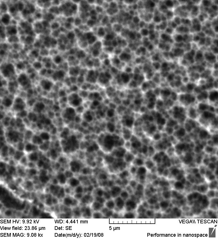 | Figure (7). The SEM image of the top surface of the nanostructured solar cell etched electrochemically under 15 mA/cm2 current density, 15 minutes etching time and 10 % HF concentration |
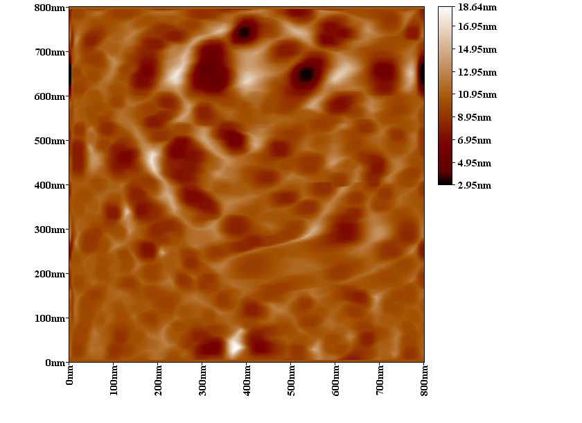 | Figure (8). The SPM image of the nanostructured solar cell etched by electrochemical etching techniqueunder 15 mA/cm2 current density, 15 minutes etching time and 10 % HF concentration |
4. Conclusions
Surface texturing and reconstruction of an ordinary solar cell could enhance the light absorption and then the conversion efficiency of the nanostructured solar cell. The solar cell efficiency is affected by two important parameters; the etching time and the current density. The electrochemical etching process can be performed on the solar cell surface without affecting the cell junction. The Raman and photoluminescence spectroscopy indicate existence of silicon nanostructures. Pore-like structure of small pores separated by thin wall could be formed at the top of solar cell by electrochemical etching of ordinary solar cell.
References
| [1] | A. Luque, and A. Martí, Progress in Photovoltaics, vol. 9 (2001) p. 73-86. |
| [2] | J.Carey, What’s raining on solar’s parade, Business Week, February 6, (2006). |
| [3] | C.B. Honsberg,”Approaches for Ultra-High Efficiency Solar Cells,” Proceedings DOE Solar Program Review, November, (2004). |
| [4] | W.Hoffman, Sol.Energy Mater&Sol.Cell 90(2006) 328. |
| [5] | A.Shalav, B.S.Richards, M.A.Green, Sol.Energy MaterSol.Cells 91 (2007) 82. |
| [6] | C.Korman, Overview of solar photovoltaic markets and technology, Cornell University, March 28(2006). |
| [7] | Zh. Nansheng, M. Zhongquan, Zh. Chengyue and H. Bo, J. Semiconductors, 30 (2009) 7. |
| [8] | K. Drabczyka, P. Panekb, M. L. Nskib, Solar Energy Materials & Solar Cells, 76(2003). P.545-551. |
| [9] | A. G. Cullis, L. T. Canham, and P. D. Calcott, J. Appl. Phys., 82 (1997) 909. |
| [10] | W. Calleja, R. Osario, C. Vasquez, S. Quintana and C. Falcony, Super lattices Vac. 9 (1999) 239. |
| [11] | P. A. Kohl, Appl. Phys. Lett,73 (1998) 1577. |
| [12] | C. Ossadnisk and V. Veprek, Thin Solid Films, 337 (1999) 148. |
| [13] | H. Richter, Z. Wang and L. Ley, Solid State communication 39 (1981) 625. |
| [14] | F. Kozlowski, J. Bernard and L. Koker, Material Science & Engineering B69-70 (2000) 157. |
| [15] | C.Bonafos, B.Colombeau, A.Altibelli, M.Carrada, Nucl.Instrum.Methods B 178 (2001)17. |
| [16] | V.Svrcek, A.Slaoui, J.C.Muller, Thin Solid Films 451– 452 (2004) 384. |
| [17] | Daniel Minoli'' nanotechnology applications” John Wiley & Sons, Inc. (2006) New Jersey. |
| [18] | I. Campbell and P. Fauchet, Solid State Communication 58 (1986) 739. |
| [19] | T. Suemoto, K.Tanaka and A. Nakajima, Phys. Rev. Letts. 70 (1993)3659. |
 Abstract
 Reference
 Full-Text PDF
 Full-Text HTML