-
Paper Information
- Next Paper
- Previous Paper
- Paper Submission
-
Journal Information
- About This Journal
- Editorial Board
- Current Issue
- Archive
- Author Guidelines
- Contact Us
Nanoscience and Nanotechnology
p-ISSN: 2163-257X e-ISSN: 2163-2588
2012; 2(6): 159-163
doi: 10.5923/j.nn.20120206.02
Radiation Effects in Nano Inverter Gate
 Abstract
 Reference
 Full-Text PDF
 Full-Text HTML
Nooshin Mahdavi
Sama Technical and Vocational Training College, Islamic Azad University, Tehran Branch, Tehran, Iran
Correspondence to: Nooshin Mahdavi, Sama Technical and Vocational Training College, Islamic Azad University, Tehran Branch, Tehran, Iran.
| Email: |  |
Copyright © 2012 Scientific & Academic Publishing. All Rights Reserved.
Quantum Cellular Automata (QCA) represents an emerging technology at the nanotechnology level. The effects of space radiations in QCA inverter gate are investigated in this paper. Single Electron Fault (SEF) is a fault which may happen during operation of QCA circuits. A detailed simulation based logic level modelling of Single Electron Fault for QCA inverter gate is represented in this paper. It will be shown that the behaviour of single electron fault in QCA devices is not similar to either previously investigated faults or conventional CMOS logic
Keywords: Space Radiation, Quantum Cellular Automata, Inverter Gate
Cite this paper: Nooshin Mahdavi, "Radiation Effects in Nano Inverter Gate", Nanoscience and Nanotechnology, Vol. 2 No. 6, 2012, pp. 159-163. doi: 10.5923/j.nn.20120206.02.
Article Outline
1. Introduction
- The microelectronics industry has improved the integration, the power consumption, and the speed of integrated circuits during past several decades by means of reducing the feature size of transistors. But it seems that even by decreasing the transistor sizes, some problems such as power consumption can't be ignored. Utilizing the QCA technology for implementing logic circuits is one of the approaches which in addition to decreasing the size of logic circuits and increasing the clock frequency of these circuits, reduces the power consumption of these circuits. QCA, which was first introduced by Lent et al.[1], represents an emerging technology at the nanotechnology level. QCA cells have quantum dots, in which the position of electrons will determine the binary levels of 0 and 1.Various types of cell misplacement faults may occur during fabrication and manufacturing of QCA devices and circuits. Some of them which have been characterized are cell displacement, cell misalignment, cell omission and cell rotation[2-7]. ◆ A cell displacement is a defect in which the defective cell is misplaced from its original direction.◆ A cell misalignment is a defect in which the direction of the defective cell is not properly aligned.◆ A cell omission is a defect in which a particular cell is missing compared to the original.◆ A cell rotation is a defect in which the defective cell is rotated in its location.There are some other faults, such as missing or extra dots or/and electrons which may occur in QCA devices and such circuits[2, 3]. Single event effects (SEE) are an example of phenomena which can affect QCA devices and circuits. These types of effects can cause electrons to tunnel outside or inside QCA cells, and therefore some remaining QCA cells may contain zero, one, two, three, four or more electrons. This is the main defect caused by SEEs which may occur for QCA devices and circuits. Considering the QCA structure with two electrons in each cell, we can conclude that defected cells may lead to circuit malfunctioning[8].Nanoelectronic devices are very sensitive to the space environment radiations. The presence of high-energy particles such as protons, heavy ions and electrons, may lead to many hazardous effects. These effects include reduction in performance or functional disruptions that can affect any system operations. This can make satellites experience shortened lifetime or major failures. The main goal of this paper is to model and characterize the single electron fault in QCA inverter gate. This fault may happen in presence of high-energy particles.The remainder of this paper is as follows. In Section 2, a brief review of QCA is presented. The radiations in the natural space are explained in Section 3. In Section 4, the effects of single electron fault on QCA inverter gate are investigated. Finally, Section 5 concludes this paper.
2. Quantum Cellular Automata
- In Quantum Cellular Automata (QCA), a cell contains four quantum dots, as schematically shown in Figure 1. The quantum dots are shown as the open circles which represent the confining electronic potential. Each cell is occupied by two electrons which are schematically shown as the solid dots.In a cell, the electrons are allowed to jump between the individual quantum dots by the mechanism of quantum mechanical tunnelling but they are not allowed to tunnel between cells. The barriers between cells are assumed sufficient to completely suppress intercellular tunnelling.
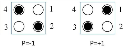 | Figure 1. QCA cell and its ground states |
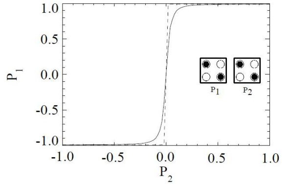 | Figure 2. Coupling of QCA cells |
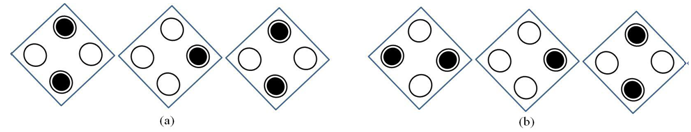
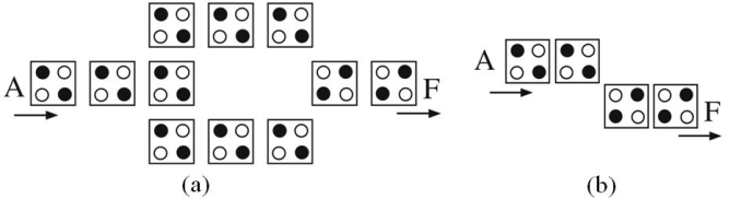 | Figure 3. (a) Redundant inverter gate and (b) Inverter gate |
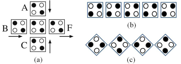 | Figure 4. (a) Majority logic gate, (b) Binary wire, and (c) Inverter chain |
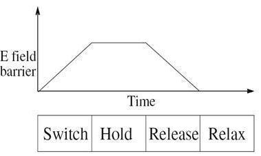 | Figure 5. Barrier height in four phases of clock |
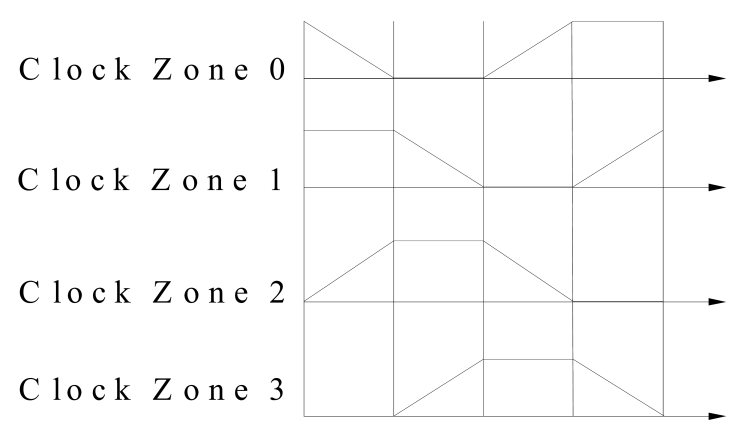 | Figure 6. QCA clock zones |
3. Radiation in the Natural Space
- The high-energy ionizing particles of the space environment are responsible for the anomalies observed on electronics.They can be classified in three categories depending on their origin[16]. Figure 7 illustrates the various space radiations.◆The radiation belts: charged particles like electrons (up to 30 MeV) and protons (up to 500 MeV) are trapped by the earth magnetic field leading to “stable” and hazardous zones in the near earth vicinity. (The Van Allen belts) ◆Solar flares: protons (up to 500 MeV) and heavy ions in a lesser extend (up to 10 MeV/nucleon) can be emitted during these solar events. The flare occurrence is influenced by the solar cycle: much more event are observed during the so-called “solar maximum” periods.◆The cosmic rays: they are a continuous background of ions whose energy levels can be very high. The origin of cosmic rays lies outside the Solar System. Shock waves and interstellar electromagnetic fields scatter and accelerate ions that can reach thousands of GeV (significantly higher than those observed during solar flares).These particles produce various effects when interacting with electronic devices.Considering a QCA cell, it contains four quantum dots and two electrons which can tunnel between dots. As mentioned before, the barriers between cells are assumed sufficient to completely suppress intercellular tunnelling. References (such as[10]) emphasize that this barrier height is less than 1 eV. Considering the ionizing particles which may have several MeV to several GeV of energy, this energy can motivate at least 10 million electrons to tunnel outside or inside QCA cells. But according to the size of cells and the effective area of that particle's affection, these motivated electrons are much less. Here we do not want to count the number of electrons which can tunnel outside or inside of QCA cells in presence of an ionizing particle, but we want to investigate the effect of this phenomenon and defects which may occur for QCA cells. After tunnelling of some electrons outside or inside QCA cells, some remaining cells may contain zero, one, two, three, four or more electrons. This is the main defect which may occur for QCA cells and circuits.
4. Fault Modeling
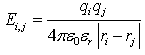
- In this Section, fault modelling will be accomplished for QCA Inverter gate. All cells are assumed to have a length and width of 18 nm and quantum dots are 5 nm in diameter. The centre to centre distance of two neighbour cells is 20 nm. Thus, the cell size can be defined as 20 nm. As an assumption, a 20 nm cell size was used in[16] and a 25 nm cell size was used in[5]. Thus, the 20 nm assumption is valid for QCA cells. The centre to centre distance of two neighbour quantum dots in a QCA cell is 9 nm (For example, dot1 and dot2 in Figure 1). According to previous definitions, other geometric distances are calculated. As an example, considering two neighbour cells, the distance between dot4 in the left cell and dot1 in the right cell is 29 nm and so on.Also it is assumed that each cell is assigned to an individual clock zone and there are no neighbour cells with the same clock zone. Positions of electrons and polarization of cells are obtained from the fact of the least Kink energy. The Kink energy (electron volt) can be computed by the following equation.
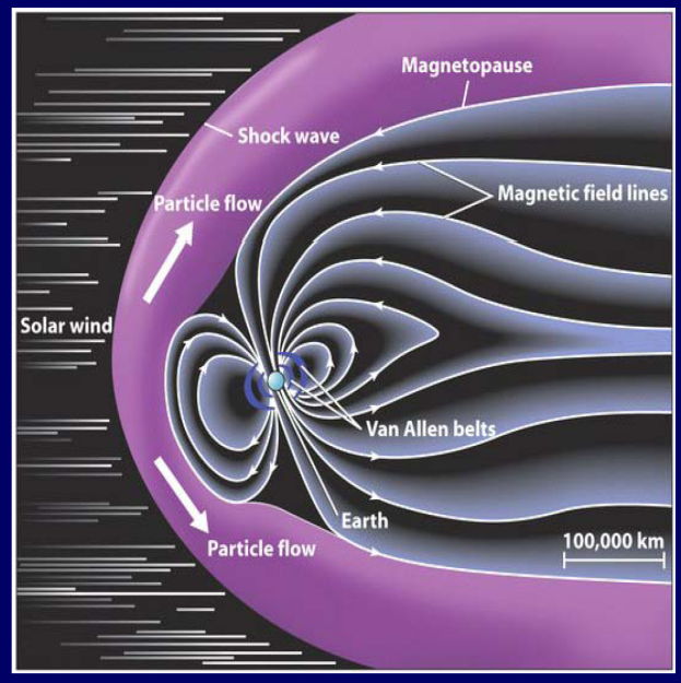 | Figure 7. Radiation Belts, Solar Flares, and Cosmic Rays |
 | (1) |
|
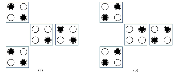
 | Figure 8. Faulty cell effect on inverter chain |
|
 | Figure 9. Output faulty cell effect on redundant inverter gate |
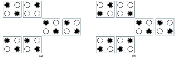 | Figure 10. Up input faulty cell effect on redundant inverter gate |
|
5. Conclusions
- Space particles such as protons, heavy ions and electrons can produce various faults when interacting with nanoelectronic devices.A detailed modelling and characterization of single electron fault for QCA inverter gates has been represented in this paper. As stated before, the behaviour of single electron fault in QCA devices is not similar to either previously investigated faults or conventional CMOS logic. For example, stuck at zero or stuck at one fault model in redundant inverter gate is based on the input on which the fault occurs.
References
| [1] | C. S. Lent, P. D. Tougaw, W. Porod, and G. H. Bernstein, ”Quantum Cellular Automata,” Nanotechnology, Vol. 4, No. 1, pp. 49-57, 1993. |
| [2] | M. B. Tahoori, J. Huang, M. Momenzadeh, F. Lombardi, ”Testing of Quantum Cellular Automata,” IEEE Trans. on Nanotechnology, Vol. 3, No. 4, pp. 432-442, Dec. 2004. |
| [3] | M. Momenzadeh, M. B. Tahoori, J. Huang, F. Lombardi, ”Quantum Cellular Automata: New Defects and Faults for New Devices,” in 18th International Parallel and Distributed Processing Symposium, 2004. |
| [4] | M. Momenzadeh, J. Huang, F. Lombardi, ”Defect Characterization and Tolerance of QCA Sequential Devices and Circuits,” in 20th IEEE International Symposium on Defect and Fault Tolerance in VLSI Systems, 2005. |
| [5] | M. Momenzadeh, J. Huang, M. B. Tahoori, F. Lombardi, ”Characterization, Test, and Logic Synthesis of And-Or-Inverter (AOI) Gate Design for QCA Implementation,” IEEE Trans. on Computer-Aided Design of Integrated Circuits and Systems, Vol. 24, No. 12, pp. 1881 - 1893, Dec. 2005. |
| [6] | J. Huang, M. Momenzadeh, M. B. Tahoori, F. Lombardi, ”Defect Characterization for Scaling of QCA Devices,” in 19th IEEE International Symposium on Defect and Fault Tolerance in VLSI Systems, 2004. |
| [7] | P. Gupta, N. K. Jha, L. Lingappan, ”A Test Generation Framework for Quantum Cellular Automata Circuits,” IEEE Trans. on VLSI Systems, Vol. 15, No. 1, pp. 24-36, Jan. 2007. |
| [8] | M. Mahdavi, M. A. Amiri, S. Mirzakuchaki, ”SEU Effects on QCA Circuits,” Proceedings of International Conference on Test and Diagnosis, China, Apr. 2009. |
| [9] | P. D. Tougaw and C. S. Lent, ”Dynamic Behavior of Quantum Cellular Automata,” J. Appl. Phys., Vol. 80, No. 8, pp. 4722-4735, Oct. 1996. |
| [10] | P. D. Tougaw, C. S. Lent, and W. Porod, ”Bistable Saturation in Coupled Quantum-dot Cells,” J. Appl. Phys., Vol. 74, No. 5, pp. 3558-3565, Sep. 1993. |
| [11] | P.D. Tougaw and C.S. Lent, ”Logical Devices Implemented Using Quantum Cellular Automata,” J. Appl. Phys., Vol. 75(3), pp. 1818-1825, 1994. |
| [12] | M. A. Amiri, M. Mahdavi, S. Mirzakuchaki, ”QCA Implementation of a Mux-Based FPGA CLB,” in International Conference On Nanoscience and Nanotechnology, Australia, Feb. 2008, pp. 141-144. |
| [13] | K. Hennessy and C. S. Lent, ”Clocking of Molecular Quantum-dot Cellular Automata,” J. Vac. Sci. Technol., Vol. 19, No. 5, pp. 1752-1755, Sep. 2001. |
| [14] | K. Kim, K. Wu, R. Karri, ”The Robust QCA Adder Designs Using Composable QCA Building Blocks,” IEEE Trans. On Computer-Aided Design of Integrated Circuits and Systems, Vol. 26, NO. 1, Jan. 2007. |
| [15] | V. Vankamamidi, M. Ottavi, F.Lombardi, ”Two-Dimensional Schemes for Clocking/Timing of QCA Circuits,” IEEE Trans. on Computer-Aided Design of Integrated Circuits and Systems, Vol. 27, No. 1, pp. 34-44, Jan. 2008. |
| [16] | Heumpil Cho and Earl E. Swartzlander, ”Adder Designs and Analyses for Quantum-Dot Cellular Automata,” IEEE Trans. on Nanotechnology, vol. 6, No. 3, pp. 374-383, May. 2007. |