Ilya A. Obukhov
Nanoelectronics TD, Korolev, 141070, Russia
Correspondence to: Ilya A. Obukhov , Nanoelectronics TD, Korolev, 141070, Russia.
| Email: |  |
Copyright © 2012 Scientific & Academic Publishing. All Rights Reserved.
Abstract
The frequency-dependence of electrical characteristics of quantum device components was researched. There were two types of nanostructures: quantum wire and junction nanostructures between two quantum wires with different cross sections. It is shown that conductivity of the first nanostructure is decreased with growth of the frequency and conductivity of the second nanostructure is increased with growth of the frequency.
Keywords:
Quantum Wire, Frequency, Conductivity
Cite this paper:
Ilya A. Obukhov , "About the Frequency-Dependence of Electrical Characteristics of Quantum Devices", Nanoscience and Nanotechnology, Vol. 2 No. 5, 2012, pp. 144-147. doi: 10.5923/j.nn.20120205.03.
1. Introduction
Interest to electrical characteristics of quantum wires is caused by new physical effects which are observed in one-dimensional conductors[1,2] and also by prospects of high-frequency applications of devices based on quantum wires[3,4].The consecutive analysis of frequency-dependence of quantum device characteristics can be conducted in the framework of a multiphase model of charge transport[4,5]. The model was successfully applied in order to calculate the characteristics of resonant-tunneling diodes and devices based on quantum wires[6,7]. In this paper, it is shown that frequency-dependence of one-dimensional electronic gas conductivity is determined by the frequency properties of the hydrodynamic velocity of electrons. In quantum devices, the junction between quantum wires with different cross-sections can be used as a source of nonequilibrium electrons[4,7]. Nonequilibrium effects lead to specific dependence of such junction conductivity from frequency of external signal.
2. Electric Current in Quantum Devices
The equation for the hydrodynamic velocity of electron v(x,λ) can be written as[4]  | (1) |
Here, the index λ numbers the possible electron states, τ(λ) and F(t,r,λ) - are the electron momentum relaxation time and electron chemical potential in λ-state. Other values, which are included in the equation (1) are determined as follows: 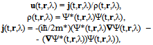 | (2) |
where ħ - is the Planck constant and electron wave functions Ψ(t,r,λ) satisfy Schrödinger’s equation | (3) |
in which m* is the electron effective mass, and potential U(t,r) is determined by the expression | (4) |
In expression (4), Uext(r) - is the built-in potential caused, for example, by the breaks of band gaps of heterostructures, e - is the electronic charge and φ(t,r) - is the self-consistent electric potential calculated by Poisson’s equation | (5) |
Where eNint(r) - is a density of doping charge. The equation (5) is fair at characteristic frequencies that are a lot of smaller than  where c – is the speed of light, and L – is the typical size of structure. For modern and perspective electronic devices, the following estimation is right
 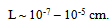 It means that the equation (5) is fair for frequencies smaller than 1014 Hz. Electron concentration n(x) and density of electron flow n(t,r) are calculated as the sums of corresponding values in λ-states
  | (6) |
where  | (7) |
 | (8) |
and 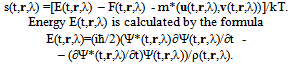 | (10) |
where k is the Boltzmann constant, T – is the absolute temperature, which in this article is a constant. In the limit of small v(t,r,λ) when the condition is right  expression for flow density will become
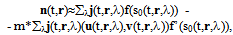 | (11) |
Where As a rule in applied tasks for every λ there will be such λ1 that
 In this case
 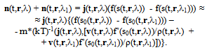 | (12) |
In expression (12), the first composed has a linear dependence on the microscopic flow j(t,r,λ) and the second composed has a quadratic dependence of this value. In a limit when we will receive
 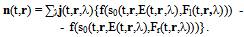 | (13) |
Here, summation on λ1 was replaced by equivalent summation on λ and designated as The distribution functions within brackets in the formula (13) differ only by the values of chemical potentials at the local chemical equilibrium when
 the flow density is zero. Thus, expression (13) describes a flow generated by local chemical nonequilibrium of charge particles. The well-known formula for a tunnel current[8] follows from the ratio (13). In case of a local chemical equilibrium, when the difference between chemical potentials of λ-phases may be neglected taking into account the formula (12) for the flow density, the following expression occurs
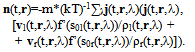 | (14) |
Here, summation by indexes λ and λ1 is replaced by summation by index λ for the "left electrons" marked by index l and the "right electrons" marked by index r. The length of chemical potentials of different electrons relaxation to local chemical equilibrium is defined by the formula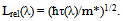 | (15) |
Size of Lrel is different for different materials. It is equal to about 10 nanometers for Si, 24 nanometers for GaAs and 72 nanometers for InSb. Where structures are larger than Lrel it is possible to conclude that the electrons are in a state of local chemical equilibrium. From the considered formulas, it follows that the current in electronic devices is created by two factors: deviations of electronic gas from the local chemical equilibrium and at nonzero values of hydrodynamic velocity of electrons. According to formula (1), the nonzero values v(t,r,λ) are caused by gradients of chemical potentials F(t,r,λ), that are deviations from chemical equilibrium of electronic gas in various spatial points. Thus, it is possible to conclude that the electronic current is the consequence of the nonequilibrium phenomena in electronic gas.
3. Frequency-Dependence of Hydrodynamic Velocity
In case when 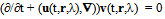 the equation (1) has the solution
 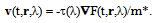 | (16) |
Substitution of expression (16) to the formula (14) results to the Ohm’s law in the differential form and to well-known formulas for mobility and conductivity of electronic gas. Let's assume that the potential difference changing in time under the harmonious law with cyclic frequency ω is applied to a spatially homogeneous sample. In this case, the gradient of chemical potential in the sample may be presented as | (17) |
where E0 – is a certain constant field. In view of spatial uniformity from (1) we shall receive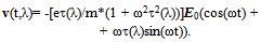 | (18) |
From (18), it follows that as well as in case of classical theory, the frequency-dependence of electronic gas conductivity becomes essential at For mesoscopic structures, the momentum relaxation time is about 10-13 s and the factor ωτ is necessary to take into account when the frequencies are more than 1 THz. Comparing expressions (13) and (16), we can see that increase of frequency results in decrease of conductivity (growth of resistance) of electronic gas. In the development of expression (18), no assumptions about quantum dimensions of electronic gas were made. It means that formulas (18) and (19) are fair for quantum wires, which represent one-dimensional conductors.
4. Frequency Influence to Resistance of Junction between Quantum Wires
For the decision of this problem, it is necessary to consider the transport equations for different electronic phases which according to[4,5] look like | (20) |
Here, values Гλλ’ and Гλ’λ are the probabilities of transitions between λ and λ’-states. In the simplest case, when only deviations from the local chemical equilibrium between "left" and "right" electrons[4,7] are taken into account, from (20) we shall receive the system of two equations | (21) |
Here: γ is some positive dimensionless constant. 
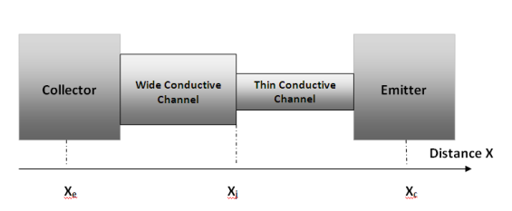 | Figure 1. The Relaxation Quantum Diode as an example of a quantum device that used the junction between two Conducted Channels of Quantum Wires as a base of functioning |
Let's consider that lengths of conducting channels of quantum wires (see Figure 1) Ll.r are much greater their cross-section sizes L┴l,r Let's in addition put that lengths L┴l,r are not less than the length of relaxation of electronic gas to the state of local chemical equilibrium
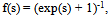
  Having made the assumptions, the nonequilibrium electronic gas is localized in the area of junction between quantum wires of different cross-sections (see Figure 2 and Figure 3). For the difference of chemical potentials
 | (22) |
we receive the approximative equation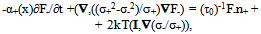 | (23) |
where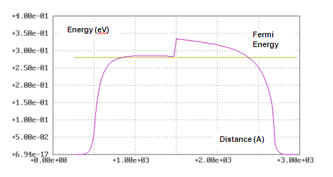 | Figure 2. The Potential Relief for electrons in Relaxation Quantum Diode (V = 0) |
 | Figure 3. Function F in Relaxation Quantum Diode (V = 0,066 V) |
Value τ0 is relaxation time of electronic gas to the state of local chemical equilibrium.From the equation (23), it follows that the source of electronic gas nonequilibrium state is the current that flows perpendicularly to boundaries of areas with different conductivities σl,r. Having made the assumptions, the equation (23) is a singularly perturbed[9]. In a stationary case, its approximate decision looks like | (24) |
As shown in[4], the value F0 is connected with the voltage drop in the device by the formula Thus, to within boundary effects[4], the ratio (24) defines the current-voltage characteristic (CVC) of junction between quantum wires with different thickness. In a one-dimensional approximation, when the total electron flow is constant for CVC of junction, we shall receive the formula
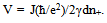 | (25) |
Here | (26) |
- is current density through the junction, d is the effective width of the junction. Value | (27) |
- is a specific resistance of the junction between two quantum wires with different cross-sections (dimension of rj is Ω*cm2). 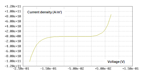 | Figure 4. Current – Voltage Characteristic of junction between two Quantum Wires with different cross-sections |
Figure 4 shows a typical CVC of such a junction. Exponential growth of current density demonstrated in the direct (right) part of the CVC is caused by exponential growth in the number of "left electrons" under conditions of voltage increasing and a corresponding decrease in potential barriers for electrons (see Figure 5). Similarly, under conditions of negative voltage, the potential barrier for electrons increases (see Figure 6), and the current does not practically flow through the junction.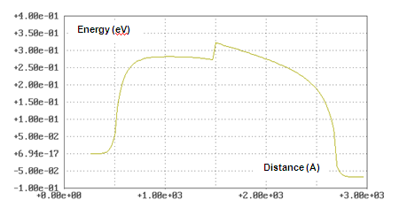 | Figure 5. The Potential Relief for electrons in Relaxation Quantum Diode (V = 0,066 V) |
If the junction is connected to the AC source, which provides the current density | (28) |
then for the CVC from the equation (23) taking into account (25), (26) and (27), the expression occurs | (29) |
Non-stationary effects become essential at | (30) |
An increase of frequency results in a decrease in junction resistance. Within the limit  the estimation is fair
 | (31) |
Voltage appears to be phase-shifted by π/2 in relation to current and effective specific resistance of the junction tends to zero with growth of frequency. 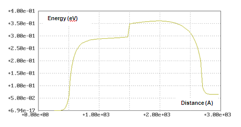 | Figure 6. The Potential Relief for electrons in Relaxation Quantum Diode (V = -0,066 V). |
At room temperature, the specified effects become essential if the frequencies exceed 1 THz. If temperature is decreased, the threshold determined by ratio (30) is decreased linearly. If temperature equals to 30 K, then frequency effects need to be considered at 10 GHz already.
5. Conclusions
In this paper, it is shown that the frequency of an external signal ω influences conductivity of quantum wires and devices based on them. Conductivity of the conducting channel of a quantum wire is decreased linearly with the growth of ω. For the junction between two conducting channels of quantum wires with different cross-sections, the inverse relationship is a representative one. Conductivity of such a junction is increased linearly with growth of the frequency, and resistance tends to zero if frequency tends to infinity. Similar frequency-dependence should be characteristic for a junction between the contact area and the conducting channel of a quantum wire.
References
| [1] | Matveev K.A. and Glazman L.I, “Coulomb blockade of tunneling into a quasi-one-dimensional wire”, Phys. Rev. Lett., v. 70, pp. 990-993, 1993. |
| [2] | Fechner A., “Frequency-Dependent Electronic Transport in Quantum Wires”, Dissertation zur Erlangung des Doktorgrades des Fachbereichs Physik der Universitat Hamburg, Germany, 2000. |
| [3] | Salahuddin S., Lundstrom M. and Datta S., “Transport Effects on Signal Propagation in Quantum Wires”, IEEE TRANSACTIONS ON ELECTRON DEVICES, v. 52, no. 8, pp. 1734-1742, 2005. |
| [4] | Obukhov I.A., Nonequilibrium effects in electronic devices, Veber (Moscow – Kiev – Minsk – Sevastopol), Russia, 2010. |
| [5] | Obukhov I.A., “The new model of charge transport in quantum devices”, in Proceeding of the Second International Conference on Nanometer Scale Science and Technology (NANO-II), pp. 889-896, Moscow, Russia, 1993. |
| [6] | Obukhov I.A., “Some aspects of nanoelectronics development in Russia”, in Proceedings of WTEC Workshop on Russian Research and Development Activities on Nanoparticles and Nanostructured Materials, pp. 85-92, S. Petersburg, Russia, 1997. |
| [7] | Obukhov I.A., “About the possibility of relaxation quantum devices creation”, Tech. Phys. Lett., v. 19, no 9, pp. 537-538, 1993. |
| [8] | Tsu R., Esaki L., Aррl. Phys. Lett., “Tunneling in a finite superlattice”, vol. 22, N 11, p.p. 562 – 564, 1973. |
| [9] | Vasil’eva A.B., Butuzov V.F. and Kalachev L.V, The Boundary Function Method for Singular Perturbation Problems, SIAM Studies in Appl. Math., SIAM, Philadelphia, USA, 1995. |
 Abstract
 Reference
 Full-Text PDF
 Full-Text HTML