Evan T. Salem
University of Technology, Applied Science Dept., laser science branch
Correspondence to: Evan T. Salem, University of Technology, Applied Science Dept., laser science branch.
| Email: |  |
Copyright © 2012 Scientific & Academic Publishing. All Rights Reserved.
Abstract
Very simple, cheap and two step method was employed for the preparation of SnO2/Si heterojunction device. SnO2 Nanoparticles was fabricated successfully using LP-PLA system, at which ablation of pure Sn metal target in DIW was done using 532.5m , 9nsec, Q-switching, Nd:YAG laser. X-Ray diffraction pattern show a Highly oriented nanostructure film related to SnO2 wurtize structure. The heterojunction device performance revealed a good rectification and photoresponce and found to be of abrupt type.
Keywords:
SnO2 Nanoparticles, LP_PLA, AFM, Heterojunction Device
1. Introduction
Nanostructured SnO2 particles was prepared using different chemical and physical methods. its important yield from its wide band gap (3.6 eV) that presents a proper combination of chemical, electronic and optical properties[1-5] also arise from Nanostructured form (which not only offers a larger surface-to-volume ratio but is also characterized by a grain size comparable to the depth of the depletion layer (few nm)) which considerably enhances their sensing performance[6] . This material found to has a broad range of important applications, ranging from solid-state gas sensors to liquid crystal displays, photovoltaic cells and transparent conducting electrodes. New effects and properties observed in the nanoscale arise mainly from surface or spatial confinement effects[10], hence, characteristics such as particle size and surface morphology play a crucial role in determining the final properties of nanostructures. For instance, it has been demonstrated that the band gap energy of semiconducting Nanocrystal is a function of particle size, when the Bohr radius is comparable to the nanocrystal size[11]. Dependent on this fact a band gap tuneable could be achieved simply by changing the particle size. using liquid phase pulsed laser ablation system( LP_PLA ) this could be achieved simply by changing the laser parameters[12]. In this work we prepared a heterojunction device using Nanoparticles colloidal, this approach has not been extensively studied yet.
2. Experimental Work
A pulsed SHG Nd-YAG laser system type (HUAFEI) providing the required laser pulses. High purity (1×1cm) (99.999) Sn plate from (Fluke) was used as a target, so it fixed at the bottom of open a plastic cell containing 3 ml dionized water (DIW) with resistivity of about 2 MW which represent the liquid media. The pure metal target was irradiated with the focused laser pulse throw (12.5 cm) focal length at specific laser fleuence of (476 J/cm2) and (40 laser pulses). The position of metal plate was continuously translated mechanically using a controlled motor. The colloidal solution vibrated for 10 min by ultrasonic vibrator in order to get homogeneity for the product, The transmittance of the films was investigated inspectral range (400–900) nm using UV-VIS Shimatzu double beam spectrophotometer .X-ray diffraction measurement has been done using Philips PW 1050 X-ray diffract meter of 1.54 Å from Cu-k. The surface morphology and particle size distributions of the Nanoparticles were analysed using atomic force microscope (AFM) from (AA3000). Heterojunction Device was fabrication Simply by Direct spraying of the SnO2 NPs colloidal using a glass nozzle connected with an air compressor on p-type Si wafer heated to about 150℃ to obtain uniform distributed Nanoparticles thin film, and hence heterojunction SnO2/ p-Si was fabricated. For devise characterization A Kiethley-616 electrometer was used to measure the flow current in a solar cell manufactured from the produced structure in dark condition as voltage been applied from a Farnell power supply of range (0.2-3) V in forward biasing and reverse biasing.
3. Result and Discussion
The optical properties of the colloidal suspension could be show in figure (1-a) where the transmission as a function of laser wavelength was measured, the average transmission found to be about (85%) , in figure (1-b), the optical absorption of the colloidal suspension show that SnO2 exaction absorption peaks locating at about (330 nm) which related to the large band gab of about (3.62 eV) as shown in figure (1-c) , the optical band gap (Eg) of SnO2 NPs is determine from extrapolating of the linear part of (αhν)2 vs. incident photon energy (hν). 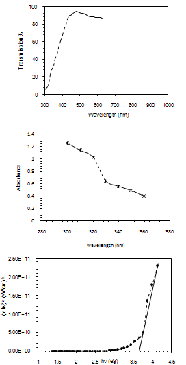 | Figure 1. optical properties a-transmission vs. wavelength b-absorbance c- (a hn)2 vs.incident photon energy |
The XRD pattern of the SnO2 NPs is shown in figure (2) were a specific and sharp peak appear due to the diffraction from the (101) plane of the SnO2 Nanoparticles, which related to 2=30.7633 diffraction angle with a corresponding lattice constant of (2.90o). There are no similar result since all the obvious work give a polymorph structure , in this work we related the wide single peak to the diffraction from the condense Nanoparticles which formed the SnO2 film on the glass substrate, This diffraction peak related to the wurtize structure of SnO2 according to the ASTM standards.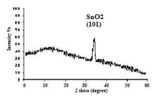 | Figure 2. x-ray diffraction pattern of SnO2 Nanocolliodal condense on glass substrate |
Figure (3) show the surface morphology of the colloidal suspension prepared by drop drying on glass substrate, it’s clearly obvious the plasma is intense enough to achieve its long life time and high temperature. in such a conditions, the space asymmetry of distributions is no longer predominant because the plume region is filled with a high density of species, Here the influence of aligned media will be much slighter, As a result the grain size increase and it shape close to a helical structure this result similar to other work[13, 14] the average grain size found to be about (102 nm) while the RMS value about ( 18 nm).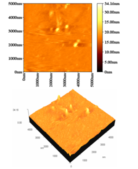 | Figure 3. surface morphology of the colliodal supention preperd by drop drying |
Direct spraying of the SnO2 NPs colloidal using a glass nozzle connected with an air compressor on Si wafer heated to 150℃ the AFM results show uniform distributed of the Nanoparticles on the substrate, as shown in the following figure (4). The averge grain size found to be about 98.2 nm while the RMS value about (0.13)nm, the difference in particle size and surface rougness related to the the uniform growth and distrubution of the nanoparticle on the substrate surface at higher tempreture.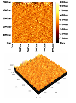 | Figure 4. AFM results of dirct sprying SnO2 colliodal suspansion prepared by sprying |
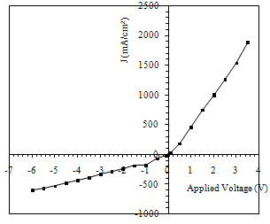 | Figure 5. I-V charechtersitic of SnO2/Si heterojunction device |
By sprying the colliodal suspension on the Si substrate a heterojunction (SnO2/ p-Si ) was obtained. Figure (5) decribe the results of the current-voltage (I-V) measurements in the dark for the prepared heterojunctions in the forward and reverse bias These characteristics are very important to describe the device performance and all device parameters depending on it. In forward biase, Two regions are recognized; the first one represents recombination current the first current established when the concentration of the generated carrier be larger than the intrinsic carrier concentration (ni), i.e. (n*p>ni2),which lead to recombination process for mass low applicable . The second region at high voltage represented the diffusion or bending region which depending on series resistance, In the reverse bias, It is clear that the curve contains two regions; the first is the generation region where the reverse current is slightly increased with the applied voltage and this leads to generate electron-hole pairs at low bias. In the second region, a significant increase can be recognized the reverse bias is increased. In this case, the current is resulted from the diffusion of minority carriers through the junction. We can also note from this figure the rapid increment in the reverse current at high reverse voltage, which is probably due to the leakage current arising from the surface layer.Figure (6) gives the 1/C2-V measurements for prepaerd device. Results show that the device capacitance is inversely proportional to the bias voltage. 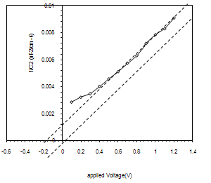 | Figure 6. photo I-V charecteristics under reverse bias for SnO2\Si heterojunction device |
The reduction in the device capacitance with increasing bias voltage resulted from the expansion of depletion layer with the applied voltage. The depletion layer capacitance refers to the increment in charge per unit area to the incremental charge of the applied voltage. This properly gives an indication of the behavior of the charge transition from the donor to the acceptor region, which was found to be "abrupt" which is confirmed by the relation between 1/C2 and reverse bias being a straight line. The photocurrent is a very important in photodetector and heterojunctin performance, The current-voltage (I-V) measurements in the illumination for SnO/p-Si heterojunction is shown in figure (7) , photo electric behavior of the device under illumination condition could be recognize. It is understood that photo electric effect result from light-induced electron-hole generation at the device and particularly at the depilation region of the P-type silicon. Under external reverse bias, depilation region of the device extends and as a result, more incident photons will contribute to the electron-hole pairs generation that takes place in the depletion region. The internal electric field in the depletion region causes the electron-hole pairs to separate from each other and this bias becomes larger with the applied external bias. From the following figure, we can see the increase in the photo-current with increasing incident light intensity, where the large intensity refers to a great number of incident photons and hence large number of separated electron-hole pairs.this figure shows the behavior of the current as afunction of the applied reverse bias voltage with different illumination powers, operating the detector under external revers bias causes the deplation region to be extended so that large number of incident photon will transmited through the SnO2 layar and absorbed mainly in the deplation region, creating electron –hole pair's which incoporate in photocurrent generation. the internal electric fields in the depletion region cause separation of the electron and the holes, this electric field is much higher when the device in the reverse bias. so, when the incident power density increased large number of electron –hole pair is generated.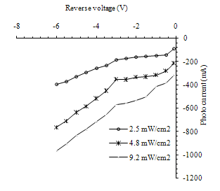 | Figure 7. photo I-V charecteristics under reverse bias for SnO2\Si heterojunction device |
4. Conclusions
According to the obtained physical properties and that have been estimated we could conclude that SnO2/Si hetrojunction device was successfully fabricated by spraying SnO2 Nanoparticles colloidal on silicon substrate. The junction show a photo responce and found to be of abrupt type. The prepared film has good uniformity and low roughness of about (0.12nm). the x-ray result show a highly oriented SnO2 film on glass substrat.
References
| [1] | Jochan Joseph, Varghese Mathew, Jacob Mathew, K. E. Abraham , Turk J Phys, 33 (2008) 37 – 47. |
| [2] | [30] Rakhi Khandelwal , Optics and Laser Technology, Volume 41, (2009), 89-93 |
| [3] | D.G. Rickerby, M.C. Horrillo, J.P. Santos, P. Serrini, Nanostruct.Mater.9 (1997) 43. |
| [4] | JCPDS (Joint Committee for Powder Diffraction Standards)Data Cards, 72-1012 and 72-2324, International Center of Diffraction Data, Swarthmore, PA, (1995). |
| [5] | C. Bouvy and B. L.Suy" ZnO@Porous Media, Their PL and Laser Effect "J. Mater. Sci. Technol., vol.24 no.4, (2008). |
| [6] | A.P. Alivisatos, J. Phys. Chem. 100 (1996) 13226. |
| [7] | Ph. Avouris, MRS Bull. 29 (2004) 403. |
| [8] | S.V. Gaponenko, Cambridge University Press,Cambridge, 1998. |
| [9] | C. Bouvy and B. L.Suy" ZnO@Porous Media, Their PL and Laser Effect "J. Mater. Sci. Technol., vol.24 no.4, 2008. |
| [10] | L. Brus, J. Phys. Chem. 90 (1986) 2555. |
| [11] | R. A. Ismail , A. K. Ali , Mukhlis M. Ismail ,K. I. Hassoon, Appl Nanosci ,vol. 1, (2011), 45–49 |
| [12] | C. Liang; "laser ablation and nanoparticle generation in liquid" Chinese of Academy of Sciences, CN,www.myeos.org/angel010 Angel,( 2010). |
| [13] | H.Usui, Y.Shimizu,T. Sasaki, and N. Koshizaki, J. Phys. Chem. B, vol. 109, (2005),120-124,. |
| [14] | T. Sasaki, Y. Shimizu, N. Koshizaki Journal ofPhotochemstry and Photobiology A: Chemistry, vol. 182, (2006),335–341,. |
| [15] | T. sasaki, C. liang, W.t. Nichols Y. shimizu, N. koshizaki, Appl. Phys. A, vol.79, 2004,1489–1492. |
| [16] | F.Mafun´e, J. Kohno, Y. Takeda, T. Kondow, H. Sawabe: J. Phys. Chem. B 104, vol. 8333, (2000). |
 Abstract
 Reference
 Full-Text PDF
 Full-Text HTML