-
Paper Information
- Next Paper
- Previous Paper
- Paper Submission
-
Journal Information
- About This Journal
- Editorial Board
- Current Issue
- Archive
- Author Guidelines
- Contact Us
Nanoscience and Nanotechnology
p-ISSN: 2163-257X e-ISSN: 2163-2588
2012; 2(3): 75-81
doi: 10.5923/j.nn.20120203.06
Investigation of Strain and Wetting in Porous Silicon and Feasibility of an Optical Sensor for Chemical Monitoring
 Abstract
 Reference
 Full-Text PDF
 Full-Text HTML
M. A. Ferrara, L. Sirleto
Istituto per la Microelettronica e Microsistemi (IMM), Consiglio Nazionale delle Ricerche (CNR), Via P. Castellino 111, Naples-80131, Italy
Correspondence to: L. Sirleto, Istituto per la Microelettronica e Microsistemi (IMM), Consiglio Nazionale delle Ricerche (CNR), Via P. Castellino 111, Naples-80131, Italy.
| Email: |  |
Copyright © 2012 Scientific & Academic Publishing. All Rights Reserved.
Abtract In this paper an experimental study of wetting phenomena in porous silicon by Raman scattering is reported and the feasibility of an optical sensor for chemical monitoring is addressed. First, a systematic study of strain effects in ‘as formed porous silicon layers’ of different porosity and thickness is described. Samples of greater thickness (20 µm) and higher porosity (70%) have been individuated as the best candidates for the observation of wetting phenomena. Then, an experimental investigation of wetting phenomena in PS layers by Raman scattering is reported. The experimental results prove a reversible blue-shift of PS Raman speak of wetted porous silicon layers by isopropanol or ethanol with respect to unperturbed layers. We ascribe the shift to a compressive stress due to the increased lattice mismatch between the porous silicon layer and the bulk silicon substrate in wetting conditions. Finally, the feasibility of an optical sensor for chemical monitoring, using an approach based on porous silicon wetting and Raman scattering measurements is discussed. We conclude that being the measured shift of Raman peak very small, this mechanism could be not useful ‘as a transducer’ for sensing application i.e. to monitor vapors and liquids in an environment.
Keywords: 78.39.j Raman spectra, 81.05.Rm Porous materials, 68.35.Gy strain, 68.08.Bc wetting
Article Outline
1. Introduction
- Porous silicon (PS) is a material of great interest for the study of fluid-solid interfacial phenomena. In fact, the high specific area (600 m2/cm3 for low level doping, p-type samples)[1] and the great reactivity of the porous layer allow its use as a base for detection of vapors and liquids[2-5].Porous silicon films can be strained and this can often cause mechanical curling and fracture. The origin of these intrinsic tensile or compressive stresses is related to the porous microstructure, i. e. the size and the shape of the silicon crystallites in PS. Direct pictures of the PS structure can be obtained by electron microscopy, but sample preparation is destructive and can modify the observed structures. Raman scattering experiments[6] and X-ray diffraction[7], being not destructive, have been performed in order to obtain a better knowledge of the structural properties of PS, too. For an as-formed porous silicon sample, strain depends on various parameters, the most important being the porosity of the PS layer, the type and the level of doping of the silicon substrate[8,17]. On top of layer the PS lattice parameter is slightly expanded in direction perpendicular to the surface, while in direction parallel to the surface, the porous layer has the same lattice parameter as the substrate[8,10]. Yang et al. [6] investigated the built-in strain of a PS layer by top surface Raman scattering. They proved that a dilatation strain of the order of 10-3 gives an additional decrease of a few cm-1 of the 520 cm-1 optical mode, improving the agreement of the theoretical fit with the experiment results. When PS layer is attached to Si substrate, moving from top to bottom, due to lattice mismatch with bulk Si, a PS layer is expected to be under compressive stress[9]. It is well known that along the thickness of the films, the position of the Raman peak is the result of a competition between confinement effects which cause a red shift of the peak position with respect to bulk Si, and compressive stress induced by lattice mismatch with Si substrate, which causes a blue shift of the peak. Thus, according to the data reported in ref.[18-21], it may hypothesize gradients of intrinsic stress along the thickness of the films. Cross sectional micro-Raman studies report a compressive stress at the interface with the substrate, which can be directly attributed to the lattice mismatch[18-21].The behaviour of a fluid confined in mesoporous media, which exhibit pore size in the range 2-50 nm, still arouses a great interest because it concerns materials which could have a lot of applications[22]. Besides, from a fundamental point of view, the study of adsorption and condensation processes allow to get information about the microscopic structure and composition of porous materials[23,24]. Adsorption and wetting phenomena are due to molecular interactions between a fluid and an adsorbent, which is usually considered to be rigid[10]. However, the adsorbent also experiences the action of the molecular forces, causing substrate deformations, as indeed has been revealed by observations of strains induced by adsorption and wetting process[10 and references therein].Measurements of adsorption strains in PS are of great interest, because it is a unique example of a crystalline porous material having the structural properties of a nearly perfect crystal[25]. In porous silicon, due to the large internal surface, the strain is very sensitive to oxidation, to the presence of a fluid or to impregnation with various substances. Since the pores are in the nanometer range, the presence of any fluid inside the pore network leads to a lattice variation detectable, for example, by X-ray diffraction[4,5,26,27] A small increase of strain is observed when a p+ type PS layer is filled with a liquid[27], while for vapor adsorption a small decrease of strain has been observed when capillary condensation occurs in the pores[4]. After evaporation, these effects are usually reversible.Raman scattering is an emission technique that involves inelastic scattering of incident laser photons and results in spectral peaks that are shifted from the incident light. The Raman bands arise from changes in the polarization density during crystal or molecule vibrations. As a result, Raman scattering allows the determination of the fingerprint of the species present and it is structurally specific. From this point of view, it is an innovative, powerful, non-destructive and non-contact detection technique, capable of giving results in those applications where standard spectroscopic techniques are less effective or difficult to use, such as the monitoring of toxic vapours, explosive, or metal ions[28]. One of the most interesting characteristics of Raman scattering is sensitivity to strain in the sample[29], when the material is under strain, its Raman wave will shift or deform from the original status, then this mechanical quantity is possible to be directly measured. It is well know that compressive stress results in the shift of the position of the Raman peak towards higher cm-1 (commonly called “blue shift”), while tensile stress results in a shift towards lower cm-1 (“red shift”)[30-32]. The aim of this paper is twofold: fundamental and applicative. Concerning Raman laser, it is well known that spectral limitation of the Raman effect in silicon is unavoidable in the SOI platform. In the case of Raman amplification, the limited bandwidth of the spontaneous Raman signal from silicon (105 GHz) makes it unsuitable for its use in broadband wavelength division multiplexing (WDM) applications, unless the multipump schemes are implemented. In our previous paper[33-36], an approach based on Raman scattering in porous silicon was investigated. Two significant advantages with respect to silicon were proved: the broadening of spontaneous Raman emission and the tuning of the Stokes shift. Therefore, in this paper, we want to investigate, from a fundamental point of view, the possibility to tune and/or to extend the Raman spectra taking advantage of wetting phenomena. Form an applicative point of view we want to investigate if the shift of the silicon Raman peak, depending on the stress profile induced in the porous layer by the wetting mechanism of the given substance, can be used as a simple mechanism to monitor the presence of vapors and liquids in an environment.In this paper, because of the aim is to study wetting phenomena, only top surfaces Raman studies are performed. First, micro-Raman spectroscopy and the spatial correlation model are used in order to observe and separate structural and strain effects in ‘as formed porous silicon layers’ of different porosity and thickness. Size of the silicon crystallites in PS samples have been calculated, too. Finally, several Raman spectra measured on unperturbed PS layers and in PS layers wetted by isopropanol or ethanol have been compared. A reversible blue shift of the PS Raman peak was observed in all spectra measured in wetting conditions.
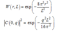
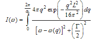
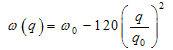
2. Theoretical Background
- The Raman effect in crystals is due to the scattering of light by the lattice vibrations[29], leading to annihilation or creation of crystal phonons. The energy lost or gained by the lattice is compensated by the increase (anti-Stokes part of the Raman spectrum) or the decrease (Stokes part of the Raman spectrum) of the energy of the scattered light. Moreover, as optical photons have very small wave vectors (approx. 105 cm-1) if compared with lattice vibrations (up to 108 cm-1), due to the conservation of the crystal momentum in the scattering process only phonons at the centre of the Brillouin zone (namely, having q=0 wavevector) can be involved in the scattering process. In crystalline silicon, the scattering of optical photons from the threefold degenerate optical phonon at the centre of the Brillouin zone gives rise to a strong Stokes peak at approximately 521 cm-1 from the laser line, having a full width at half maximum (FWHM) of approx. 4 cm-1 at room temperature.Porous silicon is composed of wires and/or dots of not uniform dimensions. When the size of the particles reduces to the order of nanometers, the wave function of optical phonons is no more a plane wave[30]. The localization of the phonon wavefunction (phonon confinement effect) leads to the relaxation of the wave vector conservation in the Raman scattering process in a crystal. Thus, not only the phonons with zero wave vector, but also those with q≠0 take part in the Raman scattering process, resulting in the red shift and broadening of the PS Raman line[30,31]. Campbell and Fauchet[30] developed a quantitative model that calculates the Raman spectrum of porous silicon as depending on the size L and on the shape of the porous silicon crystallites. If PS is modelled as an assembly of quantum wires, the phonon confinement is assumed to be two dimensional, while if the PS is modelled as an assembly of quantum dots, the confinement is three dimensional. The localization of the phonon wavefunction is imposed by means of a weighting factor W and the resulting localized wavefunction is expanded in a Fourier series with coefficients C(0,q)[30,32]. The Raman spectrum is given by:
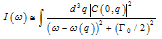 | (1) |
 | (2) |
 | (3) |
 | (4) |
3. Experimental Results and Discussion
- Unpolarized Raman spectra have been detected, at room temperature, in backscattering geometry using a Jobin Yvon Ramanor U-1000 double monochromator, equipped with a microscope Olympus BX40 for micro-Raman sampling and an electrically cooled Hamamatsu R943-02 photomultiplier for photon-counting detection. The excitation source was a Coherent Innova 70 Ar+ laser, operating at 514.5 nm wavelength. In order to prevent laser-annealing effects, the average laser power was about 2 mW at the sample surface. Using a 50X objective having long focal distance, the laser beam was focused to a diameter of few microns. Its position on the sample surface was monitored with a video camera. PS Raman spectra have been fitted to the model of Campbell and Fauchet by means of a properly designed MATLAB code. As a result of the fit, the average size of the porous silicon crystallites has been calculated. In order to estimate the modifications induced in porous silicon layers by the wetting by liquids, a significant number of spectra has been recorded. As weak variations in the Raman spectra are expected, the data analysis must be carefully carried out. To this aim, the data have been fitted not only by means of the phonon confinement model, but also by two gaussian curves[39] or by an asymmetrical line shape (Breit-Wigner-Fano function, BWF)[40].
3.1. Strain in ‘as Formed Porous Silicon Layers’
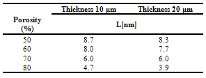
- In these experiments, porous silicon monolayers have been obtained by electro-chemical etching on p+ type (ρ=8-12 mΩ cm) standard silicon wafers (001). In order to study the effect of both porosity and thickness on the Raman spectrum of porous silicon, two series of samples having different thickness (10 m - 20 m) have been prepared. At fixed thickness, the porosity of the samples ranged between 50% and 80% (step 10%). As a preliminary measurement, the Raman spectrum of c-Si has been recorded. A lorentzian line, centred at 521.4 cm-1 and having FWHM of approximately 4.4 cm-1 was obtained. In Fig.1, the Raman spectra of 20 m thick PS samples having different porosity are shown. As expected from previous theoretical works[30,32] the shift of the PS Raman peak towards lower wavenumbers and the broadening of the line is greater in samples of higher porosity (Fig.1). By fitting the measured Raman spectra with the model proposed by Campbell and Fauchet (eq. (3)), information about the size of the silicon crystallite have been obtained. In Tab. I are listed, for each sample at a given porosity and thickness, the estimated size of the crystallite. The size of the crystallite decreases with increasing porosity. Moreover, at fixed porosity, a lower size of the crystallite is obtained in samples of greater thickness.
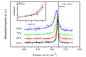 | Figure 1. (Color online) Raman spectra (circles) of PS samples (20 μm) at different porosity. In the inset, the positions of the PS Raman peaks registered on the samples with different thickness as a function of the layer porosity are shown. The solid lines are drawn as guides for the eye |
|
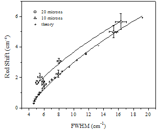 | Figure 2. Relationship between the linewidth and the peak shift of experimental and theoretical PS Raman peak with that of c-Si. The solid lines are drawn as guides to the eye |
3.2. Porous Silicon Wetting
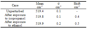
- In order to investigate wetting phenomena, unperturbed porous silicon layers and porous silicon layers wetted by by 100% liquid solutions of isopropanol or ethanol ‘were’ characterised by Raman scattering. These two liquids have been chosen because of their excellent properties of the hydrophilic interaction with Si surface ensuring very efficient nano-pores filling[11,27]. We noted that porous silicon layer was closed in a small glass vial, in which a remarkable amount of liquid was added. Therefore, even if a small quantity of liquid evaporated, because of its vapours quickly saturated the atmosphere surrounding the sample, the porous silicon layer was wetted by immersion during the entire acquisition of Raman spectra. A significant number of measurements was carried out and the fitting of experimental data was obtained according to the phonon confinement model. In adsorption measurements, the experimental set-up has been slightly modified. In fact, Raman spectra have been detected on a restricted range of wavenumber shifts, to avoid too long measurements and the consequent evaporation of the liquids. Moreover, to enhance the Raman signal, a greater slit aperture has been used, slightly affecting the Raman lineshape. Anyway, Raman spectra measured on PS layers before (unperturbed condition) and after the wetting with 100% liquid solutions of isopropanol or ethanol have been compared. A significant number of measurements has been carried out and the fitting of experimental data has been obtained according to the phonon confinement model. The values of the position of the peak obtained by the fitting procedure have been used for the calculation of the mean value of the position of the PS Raman peak in unperturbed and wetting conditions. For unperturbed porous silicon the mean value of Raman peak is 519.4±0.1 cm-1. In Fig.3 one of the PS Raman peak measured in unperturbed conditions and the mean value of the peak position obtained by the fit of several Raman peaks measured in the same conditions are reported.Afterwards, aiming at studying the influence of wetting, the PS layer has been wetted by 100% liquid solutions of isopropanol or ethanol. Several PS Raman peaks have been registered in wetting conditions. After the wetting with isopropanol, the Raman peak position has a mean value of 519.8±0.1 cm-1. Therefore a blue shift of 0.4 cm-1 of the Raman peak with respect to the unperturbed PS layer is observed. The shift disappears when isopropanol completely evaporates and unperturbed conditions are restored. An example of Raman spectrum measured after the wetting with isopropanol and the mean value of the peak position obtained by the fit of several Raman peaks measured in the same conditions are shown in Fig. 4.Due to similar values of density and surface tension of isopropanol and ethanol, the effect on the porous silicon layer induced by wetting with both liquids is expected to be quite comparable. In fact, the mean value of the Raman peak position obtained in case of wetting with ethanol is 519.9±0.2cm-1. Therefore a blue shift of 0.5 cm-1 with respect to the unperturbed PS layer is obtained. The effect is reversible also in this case. An example of Raman spectrum measured after the wetting with ethanol and the mean value of the peak position obtained by the fit of several Raman peaks measured in the same conditions are shown in Fig. 5. In Table 2 the peak position, the standard deviation and the shift are reported for each case.
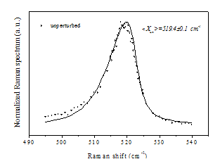 | Figure 3. Typical Raman spectrum detected on the 20 µm thick sample at 70% porosity in unperturbed (○) conditions. The solid curves represent the fit of the data with the model of Campbell and Fauchet. The average value of the peak position is also shown |
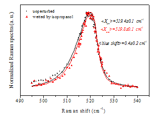 | Figure 4. (Color online) Typical Raman spectra detected on the sample at 70% porosity and 20 µm thick in unperturbed (○) and wetting (Δ) conditions. The solid curves represent the fit of the data with the model of Campbell and Fauchet. The average values of the peak positions is also shown |
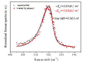 | Figure 5. (Color online) Typical Raman spectra detected on the sample at 70% porosity and 20 µm thick in unperturbed (○) and wetting (Δ) conditions. The solid curves represent the fit of the data with the model of Campbell and Fauchet. The average values of the peak positions are also shown |
|
3.3. Feasibility of an Optical Sensor for Chemical Monitoring
- In this paper, micro-Raman spectroscopy and the spatial correlation model were used to observe and separate structural and strain effects in ‘as formed porous silicon samples’ and PS layer wetted by isopropanol or ethanol. The aim was to investigate the potentiality of spontaneous Raman spectroscopy on porous silicon surfaces to measure and possibly quantify the presence of vapors and liquids in an environment. The essence of the measurement is based on the shift of the silicon Raman peak to lower or higher frequencies, depending on the stress profile induced in the porous layer by the wetting mechanism of the given substance that is being measured.According to the spatial correlation model, we estimated that PS layer could be formed by quantum dots whose size decreases with increasing porosity. Moreover, at fixed porosity, a lower size of the crystallite is obtained in samples of greater thickness. In ‘as formed porous silicon samples’, as expected, a shift of the Raman peak and a broadening of the Raman spectra with respect to c-Si is obtained. An additional red shift of the Raman peak, obtained by our experimental results with respect to the spatial correlation model, was explained, according to ref.[6], by adding a built-in strain to the phonon confinement effect. According to previous results reported in literature[4,5], a reasonable small expansion of the porous layer lattice parameter of a few 10-4 was estimated. A greater compressive stress due to the PS/c-Si lattice mismatch is observed in thinner PS samples. On the basis of our results, samples of greater thickness (20 µm) and higher porosity (70% and 80%) have been individuated as the best candidates for the observation of adsorption effects. When the PS layer was wetted with isopropanol or ethanol, a reversible blue shift, indicating the presence of a compressive stress, was observed. We ascribe the shift to a compressive stress due to the increased lattice mismatch between the porous silicon layer and the bulk silicon substrate in wetting conditions. The use of two liquids having quite similar density and surface tension, as expected, showed quite comparable blue shift. However, being the measured shift of Raman peak very small, the using of PS layer ‘as a transducer’ to monitor vapors and liquids in an environment could be not so useful for sensing application. In case of wetting of PS surface, we expect Raman peak should shift proportionally to concentration of liquid and their chemical properties (responsible for extent of strain), but being the blue shift in the presented Raman spectra very small, we believe that it could be very difficult to have a correlation between stress, presence (concentration) of liquid in PS and Raman shift.
4. Conclusions
- In this paper an experimental study of strain and wetting phenomena in porous silicon by Raman scattering is described. Samples of greater thickness (20 µm) and higher porosity (70%) have been individuated as the best candidates for the observation of adsorption effects. The results of wetting phenomena prove a reversible blue-shift of Raman spectra of wetted porous silicon layers with respect to unperturbed layers. We ascribe the shift to a compressive stress due to the increased lattice mismatch between the porous silicon layer and the bulk silicon substrate in wetting conditions. Finally, a simple mechanism which could be useful in optical sensing for chemical monitoring was elucidate and the possibility of using Raman spectroscopy and wetting of PS layers as a tool for monitoring liquids was discussed.In the future, there is an open question, which could be important to investigate from both fundamental and applicative point of view, it is to consider liquid with different surface tension. From a fundamental point of view, it is important to study if the PS microscopic structure can be influenced by liquid with different physical characteristic i. e. if it could be possible to distinguish different liquids; from an applicative point of view it is important to get a greater shift of Raman peak in order to render the approach we propose in this paper more attractive for sensing applications.