Rehana Raj T, K. Rajeevkumar
Dept of Instrumentation, CUSAT, Cochin -22, India
Correspondence to: Rehana Raj T, Dept of Instrumentation, CUSAT, Cochin -22, India.
| Email: |  |
Copyright © 2012 Scientific & Academic Publishing. All Rights Reserved.
Abstract
ZnO nanostructures were deposited on various substrates like glass, Si wafer and Al2O3/Si substrates using microwave oven based plasma deposition system at oxygen and atmospheric plasma conditions. Various morphologies were exhibited by the ZnO nanostructures grown on different substrates depending on Zinc salt concentration, plasma source and substrate material.
Keywords:
Microwave Plasma, ZnO
1. Introduction
Investigations of ZnO as a compound semiconductor were performed in the research field since last few decades due to their unique properties such as large band gap (3.37eV), high conductivity and large exciton binding energy (60meV). ZnO nanostructures have attracted the wide attention of researchers due to their performance in optoelectronics, piezoelectric applications, transparent electronics, gas sensor applications and spintronics[1]. Many researchers have synthesized ZnO by different processes like chemical vapour deposition, Atomic layer deposition, sputtering, molecular beam epitaxy, sol–gel technique etc. In this work, we have reported the synthesis of highly c-axis oriented ZnO thin films on different substrates by solvent assisted thin film deposition in plasma. We have tried to investigate the effect of different substrates and precursor concentrations on the degree of orientation and morphology of ZnO nanostructures. The proposed design in this paper is a microwave oven based remote plasma unit, which is used for solvent assisted deposition in plasma. The technique is cost effective and uses only very less precursor material. Zinc Oxide can be produced from stable salt of acetate, nitrate and chloride as reported in the literature. However, we have synthesised only zinc acetate dihydrate throughout the experimentation. X ray diffraction analysis gives details about the structure and preferred orientation planes, while SEM analysis investigates the morphology of the sample.
2. Experimental
A. Instrumentation set upFigure1 shows schematic diagram of the Domestic MW oven based Plasma deposition unit which includes (a) 2.45GHz Microwave Oven (Model HR6702D) with power source voltage ~220V/50Hz, output power consumption 700W, 17L cavity volume (b) Quartz tube chamber (c) A 12m3/lb rotary vacuum pump (d) Gas/Atmospheric feed inlet through a needle valve (e) An 8A dimmerstat to control the magnetron input voltage[2]. When the microwave radiation inside the microwave oven encounters the quartz glass tube that is filled with gas/air, the radiation can cause the gas to glow, converting the gas into electrically charged plasma. Thus plasma is created by the electrical or thermal ionization of a gas.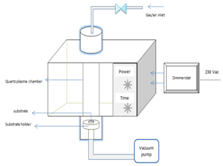 | Figure 1. Schematic diagram of Microwave Oven based Plasma deposition unit |
A constant flow of a gas / air controlled by a needle valve is provided to the quartz vacuum chamber, which is exposed to microwave frequency resulting in the partial ionisation of the gas/air. Here plasma is created in a quartz vacuum chamber at a reduced pressure typically in the order of 0.05mbar.B. Sample preparation and deposition procedureTo make the solvent for deposition, zinc acetate dihydrate, Zn (O2C2H3)2.2H2O and ethanol solution (99.5% purity) was used as precursor. Ethanolic solution of zinc acetate with concentrations 0.16M and 0.03M were prepared and deposited on three different substrates such as glass, Si wafer and Al2O3/Si wafer[3]. Standard cleaning procedures were followed for glass substrates and RCA cleaning procedure for Silicon wafer. As ethanolic solution of zinc acetate is dropped onto glass substrate, it spreads homogenously and when exposed to plasma, causes the ethanol to evaporate leaving behind the zinc salts to get deposited on glass substrate. Under plasma exposure this decomposes to ZnO and by-products as shown in equation (1) below.[16-22]. | (1) |
As plasma exposure time exceeds above 70s, there is a tendency of reducing the zinc metallic ions in the solvent to their metallic state due to free electrons in plasma.
3. Results and Discussions
The ZnO coated substrates were characterized using X-ray Diffractometry (XRD- Bruker AXS D8 Advance model, Cu Kα radiation with λ = 1.5406 A°) and Scanning electron microscopy (SEM JEOL Model JSM - 6390LV) techniques.[4,5] Material structure analysis and grain size was found using XRD and a high resolution surface imaging of the coated surface was done using SEM to study about the surface topography. Grain size could be calculated using Scherrer formula, | (2) |
Where D is the diameter of crystallite, β is full width at half maximum (FWHM) of an hkl peak at θ position, λ is the source wavelength and K = constant of proportionality which depends on crystal shape (K = 0.94 for spherical crystals with cubic symmetry). Microanalysis of elemental constituents on the coated surface was characterized using EDS (energy dispersive spectrometer) make JEOL Model JED – 2300 which was applied in conjunction with SEM analysis.A. XRD and EDS resultsWurtzite crystal structure of the ZnO are confirmed for the nanostructures formed on on different substrates such as glass, ptype Si (100) and Al2O3/Si using XRD as shown in Figures 2.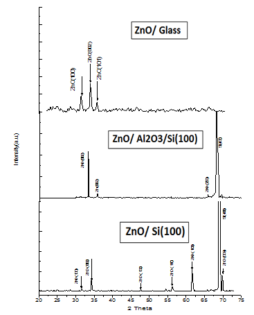 | Figure 2. XRD spectra of ZnO on different substrates |
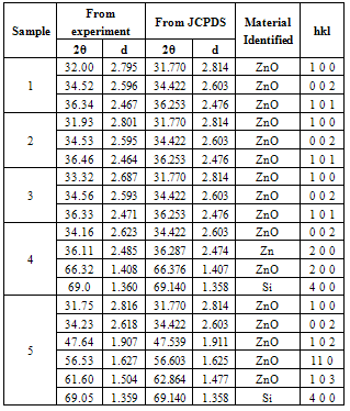
The Lattice constants (a = b = 0.32 nm and c = 0.52 nm) and prominent diffraction peaks on the planes <100>, <002> and <101> obtained from X-ray diffraction data are consistent with the JCPDS data of ZnO. A summary of obtained hkl planes, diffraction angle (2θ) in degrees and interatomic spacing (d) in angstroms is shown in Table 1 below.Table 1. Summary of XRD data
 |
| |
|
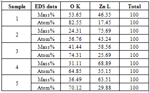
The chemical stoichiometry[6,7] of ZnO nanoparticles was investigated using EDS analysis as shown in Table 2. Table 2. Summary of EDS analysis
 |
| |
|
Zinc and oxygen constituents are found to vary with respect to air and oxygen plasma sources, precursor concentration and substrate type.A. B SEM results The SEM result shown in Figure 3(a) depicts thin film like areas with some scraps of nanoparticles spread around. Figure 3(b) shows uniform worm shaped ZnO nanostructures of size ranges 58.31nm, 70.7nm and 63.25 nm.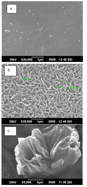 | Figure 3. SEM images of ZnO on glass substrate. (a): Precursor 0.03M, Air plasma, 70s (b) Precursor: 0.16M, Air plasma,70sec (c) Precursor: 0.16M, O2 plasma, 70 sec |
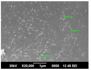 | Figure 4. SEM of ZnO on Al2O3/Si wafer |
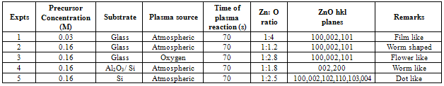
Table 3. Summary of experimental conditions and results obtained
 |
| |
|
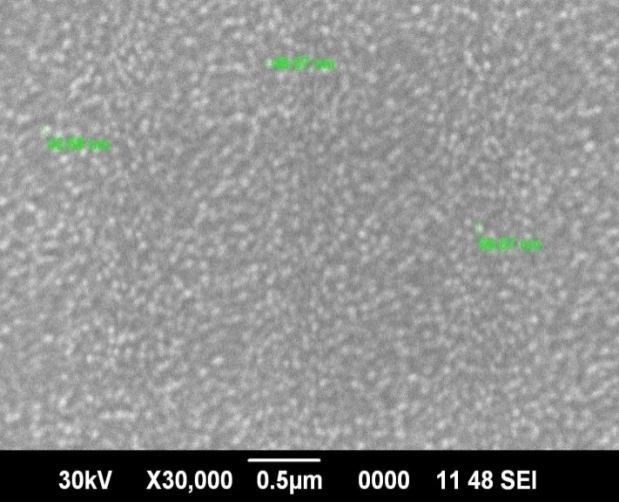 | Figure 5. SEM of ZnO on Si wafer |
Precursor concentration of 0.16M was subjected to oxygen plasma for 70s to obtain large flower shaped microstructures as shown in Figure 3(c). ZnO nanostructures formed on Al2O3/Si wafer substrate give some structures of size ranging from 70 nm to 80 nm is as shown in Figure 4. SEM images of ZnO on Si wafer substrate give uniformly distributed structures whose dimensions ranges from 42 to 66nm as in Figure 5.
4. Summary of Results
The microwave oven based plasma deposition experiments were performed to produce ZnO nanostructures at different precursor concentrations (0.03M and 0.16M), different plasma sources (oxygen and atmospheric plasma) and different substrates(glass, ptype Si(100), Al2O3/Si) as in Table 3. When precursor concentration is reduced (0.03M) , the stoichiometry of ZnO is found to be 1:4. As concentration is increased (0.16M) , the stoichiometric ratio is improved to nearly meet the expected ratio 1:1. It is known from earlier reports and reviews that ZnO can be grown in many different nanoscales. Different morphologies of ZnO nanostructures depends on factors such as influence of reactants, substrate pretreatment , growth time, temperature, influence of pH on precursor solutions , deposition time, influence of substrates, and influence of precursor concentration. On glass substrate and at atmospheric plasma, ZnO nanostructures gives film like appearance for lesser precursor concentration (0.03M) whereas worm shaped structures were grown for higher precursor concentration (0.16M).[5] Particle size of worm shaped ZnO nanostructres ranges from 58.31nm to 70.7nm showed an atomic ratio of Zn: O  1:1.2, which is closer to expected atomic ratio 1:1. On exposure to oxygen plasma, ZnO nanostructures give flower like micro structures with atomic ratio of Zn: O = 1:2.8. “Worm like” ZnO nanostructures of 70 nm to 80 nm were developed on Al2O3/Si substrate with an atomic ratio, Zn: O = 1:1.8 under atmospheric plasma exposure and 0.16M concentration. Following the same conditions as above, a more uniform spherical dot like ZnO nanostructures of 42.6nm to 66nm were developed on Si wafer substrate with atomic ratio, Zn: O = 1:2.5. The maximum intensity diffraction peak for all substrates is found to be on 002 plane. In all the three substrates , it is observed that the preferential growth is along 002 plane, which indicates that the ZnO layers were highly oriented with the c-axis perpendicular to the substrate. Different degrees of growth depends on substrate type and plasma exposure time. The prefered orientation of ZnO films synthesized by different techniques on different substrates were investigated on different literatures[8,9]. The most preferred is the (002) plane, due to its densest atomic packing and minimum surface energy. Other peaks in the XRD spectrum are formed due to plasma temperature and substrate types. XRD patterns of ZnO films deposited on a glass surface shows prominent peaks at 002 as in the reference[1] . In case of silicon substrate, peaks attributed to the (1 0 1) and(1 0 0) orientations also appear, but remain small compared to the (0 0 2) .These peaks are assumed to be due to the silicon substrate and Al2O3 deposition on Si wafer.
5. Conclusions
Future scope of work intend to analyse plasma parameters of the microwave oven based plasma to evaluate its effect on the properties of ZnO nanostructures.
References
| [1] | A. Irzh, A. Gedanken, Irzh, I. Genish, Synthesis of ZnO and Zn Nanoparticles in Microwave Plasma and Their Deposition on Glass Slides , Langmuir 26, 5976-5984 (2010). |
| [2] | C. Klingshirn, ZnO: From basics towards applications, phys. stat. sol. (b) 244, No. 9, 3027– 3073 (2007) |
| [3] | A.Irzh, I.Genish, Leon Chen, Yong-Chien Ling, Deposition of Air-Stable Zinc Nanoparticles on Glass Slides by the Solvent-Assisted Deposition in Plasma (SADIP) Method , J. Phys. Chem. C, Vol. 113, No. 32, 2009. |
| [4] | Cheng-Hsien Hsieh, Spherical Zinc Oxide Nano Particles from Zinc Acetate in the Precipitation Method , Journal of the Chinese Chem Society, 07, Vo 54, p.31-34 |
| [5] | M K Jayaraj, Aldrin Antony, and Manoj Ramachandran, Transparent conducting zinc oxide thin film prepared by off-axis rf magnetron sputtering , Bull. Mater. Sci., Vol. 25, No. 3, June 2002, pp. 227–230. |
| [6] | Ming-Guo Ma, Ying-Jie Zhu , Guo-Feng Cheng, Yue-Hong Huang , Microwave synthesis and characterization of ZnO with various morphologies, Materials Letters 62 (2008) 507–510. |
| [7] | J.Drelich,R.Zahn,J.D.Miller and J.K..Borchardt,Contact angle relaxation for ethoxylated alchohol solutions on hydrophobic surfaces, Wettability and Adhesion,Vol2,pp 253-264 |
| [8] | Teresa M. Barnes, Jacquelyn Leaf, Cassandra Fry, Colin A. Wolden, Room temperature chemical vapor deposition of c-axis ZnO, Journal of Crystal Growth 274 (2005) 412–417 |
| [9] | S. Chakrabarti, D. Ganguli, S. Chaudhuri*, Substrate dependence of preferred orientation in sol–gel-derived zinc oxide films, Materials Letters 58 (2004) 3952– 3957 |
 Abstract
 Reference
 Full-Text PDF
 Full-Text HTML