Mohammad Amin Amiri1, Sattar Mirzakuchaki2, Mojdeh Mahdavi1
1Department of Electronics, Shahr-e-Qods Branch, Islamic Azad University, Tehran, Iran
2E. E. Department, Iran University of Science and Technology, Tehran, Iran
Correspondence to: Mohammad Amin Amiri, Department of Electronics, Shahr-e-Qods Branch, Islamic Azad University, Tehran, Iran.
| Email: |  |
Copyright © 2012 Scientific & Academic Publishing. All Rights Reserved.
Abstract
Quantum Cellular Automata (QCA) is an emerging technology at the nanotechnology level. The cryptography is an interesting application of QCA technology which has not been much mentioned yet. Utilizing the QCA technology, we have implemented the A5/1 stream cipher which was the original encryption algorithm for GSM. The implementation of this cryptographic algorithm is accomplished by means of the implementation of its main modules. The main properties of the implemented modules such as latency, area and complexity are discussed in this paper.
Keywords:
Quantum Cellular Automata, A5/1, Cryptography, Implementation
Cite this paper: Mohammad Amin Amiri, Sattar Mirzakuchaki, Mojdeh Mahdavi, A5/1 Implementation in Quantum Cellular Automata, Nanoscience and Nanotechnology, Vol. 1 No. 2, 2011, pp. 58-63. doi: 10.5923/j.nn.20110102.11.
1. Introduction
The microelectronics industry has improved the integration, the power consumption, and the speed of integrated circuits during past several decades by means of reducing the feature size of transistors. But it seems that even by decreasing the transistor sizes, some problems such as power consumption cannot be ignored. Using the QCA technology for realizing logic circuits is one of the approaches which in addition to decreasing the size of logic circuits and increasing the clock frequency of these circuits, reduces the power consumption of these circuits. QCA which was first introduced by Lent et al. [1] represents an emerging technology at the nanotechnology level. QCA cells have quantum dots, in which the position of electrons will determine the binary levels of 0 and 1. A5/1 was the original encryption algorithm for GSM. This algorithm was developed in 1987. The approximate design of A5/1 was leaked in 1994, and the exact design of this algorithm was reverse engineered from an actual GSM phone by Bericeno in 1999 [2].In Quantum Cellular Automata, a cell contains four quantum dots, as schematically shown in Fig. 1. The quantum dots are shown as the open circles which represent the confining electronic potential. Each cell is occupied by two electrons which are schematically shown as the solid dots. In a cell, the electrons are allowed to jump between the individual quantum dots by the mechanism of quantum mechanical tunneling but they are not allowed to tunnel between cells. The barriers between cells are assumed sufficient to completely suppress intercellular tunneling. If they're left alone, they will meet the configuration corre-sponding to the physical ground state of the cell. It is in an obvious manner that the two electrons will tend to occupy different dots because of the Coulombic force associated with bringing them together in close proximity on the same dot. By these concepts, it is concluded that the ground state of the system will be an equal superposition of the two basic configurations with electrons at opposite corners, as shown in Fig. 1 [3, 4].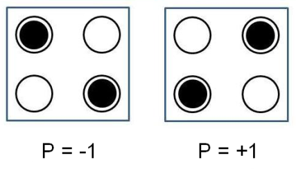 | Figure 1. QCA cell and its ground states |
The physical interactions between cells may be used to realize elementary Boolean logic functions. The basic logic gates in QCA are the Majority logic function and the Inverter gate as illustrated in Fig. 2 (a) and Fig. 2 (b), respectively. The Majority logic function can be realized by only 5 QCA cells [5]. The logic AND function can be realized through a Majority logic function by setting one of its inputs permanently to logic level 0 and the logic OR function can be implemented through a Majority logic function by setting one of its inputs permanently to logic level 1 [6]. | Figure 2. (a) Majority logic gate and (b) Inverter gate |
As an application of QCA technology, we have implemented the A5/1 stream cipher. The Section 2 will describe the A5/1 algorithm shortly. In Section 3, the implemented modules are explained and Section 4 concludes the paper.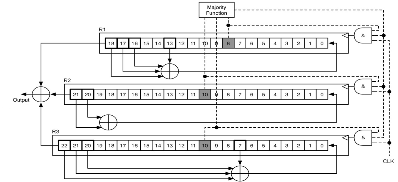 | Figure 3. A5/1 stream cipher |
2. Description of the A5/1 Stream Cipher
A5/1 was developed in 1987. As schematically shown in Fig. 3, this algorithm is built from three short linear feedback shift registers (LFSR) of lengths 19, 22, and 23 bits, which are named R1, R2 and R3, respectively. The rightmost bit in each register is named as bit zero. The taps of R1 are at bit positions 13, 16, 17, 18. The taps of R2 are at bit positions 20, 21. The taps of R3 are at bit positions 7, 20, 21, 22. When a register is clocked, its taps are XORed together, and the result is stored in the rightmost bit of the left shifted register. The three registers are specially clocked using the following majority rule: Each register has a single clocking tap (bit 8 for R1, bit 10 for R2, and bit 10 for R3). In each clock cycle, the majority function of the clocking taps is calculated and only those registers whose clocking taps are equal to the majority bit, are actually clocked [2][7-9].
3. Implementation of A5/1 Stream Cipher
 | Figure 4. Memory cell |
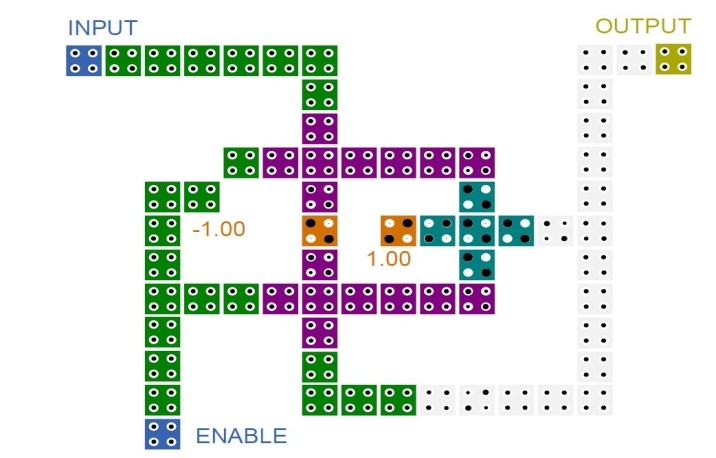
In this section, the implementation of A5/1 stream cipher is investigated by means of implementation of its main blocks. One of its main blocks is the memory cell. We have implemented a Loop-Based memory cell which has a write enable input, an input and an output. QCA implementation of this unit is illustrated in Fig. 4. It can be seen that if the ENABLE input has a high logic value, the stored memory datum will remain unchanged and if the ENABLE input has a low logic value for a period of clock, the INPUT value will be stored in the memory cell. The OUTPUT will display the stored value in the memory cell in all clock periods.Another main block of the A5/1 stream cipher is the Majority function. The Majority function produces the enable signals for shifting the A5/1 registers. This is accomplished by using the clocking bits of three predefined registers. If the clocking bit of a register is equal to majority of three clocking bits, that register should be shifted in the next operation. QCA implementation of this function for R2 register is illustrated in Fig. 5. The other Majority functions for R1 and R3 registers are almost the same as this one. This implementation has a latency of three clock periods, a complexity of 152 cells and an area of about 168000 nm2.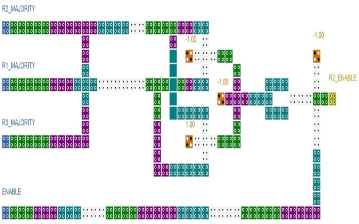 | Figure 5. Majority function |
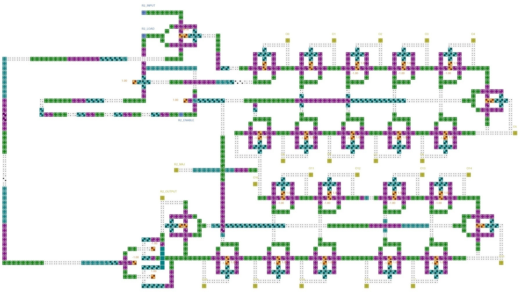
Fig. 6 shows the QCA implementation of the R1 register. This register has 19 memory cells. There are also three XOR gates and a multiplexer in R2 register. The multiplexer is used to select the R1-INPUT when the R1-LOAD is activated. Otherwise, the feedback value is selected. The 8th bit of this register is the clocking bit and the 18th bit is the output bit. The feedback of this register is computed by 13th, 16th, 17th and 18th bits which are XORed. When the R1-LOAD input has the logic value of one, the R1-INPUT value will be stored in the 0th bit of R1 register. The R1-ENABLE input is used to shift the data throughout the R1 register. When this input has the value of one for a clock period, all bits of R1 register, except 0th bit, will store the previous bit's value after five clock periods of latency. The value of 0th bit will be changed after seven extra clock periods because its feedback value should be computed by three XOR gates and the XOR gates have a total latency of seven clock periods. It means that a shift operation will be accomplished in twelve clock periods. The implementation of the R1 register has a complexity of 1589 cells and an area of about 3.24 µm2.Fig. 7 shows the QCA implementation of the R2 register. This register has 22 memory cells. There are also an XOR gate and a multiplexer in R2 register. The multiplexer is used to select the R2-INPUT when the R2-LOAD is activated. Otherwise, the feedback value is selected. The 10th bit of this register is the clocking bit and the 21st bit is the output bit. The feedback of this register is computed by 21st and 20th bits which are XORed. When the R2-LOAD input has the logic value of one, the R2-INPUT value will be stored in the 0th bit of R2 register. The R2-ENABLE input is used to shift the data throughout the R2 register. When this input has the value of one for a clock period, all bits of R2 register, except 0th bit, will store the previous bit's value after five clock periods of latency. The value of 0th bit will be changed after four extra clock periods because its feedback value should be computed by an XOR gate and the XOR gate has the latency of four clock periods. It means that a shift operation will be accomplished in nine clock periods. . The implementation of the R2 register has a complexity of 1503 cells and an area of about 2.664 µm2.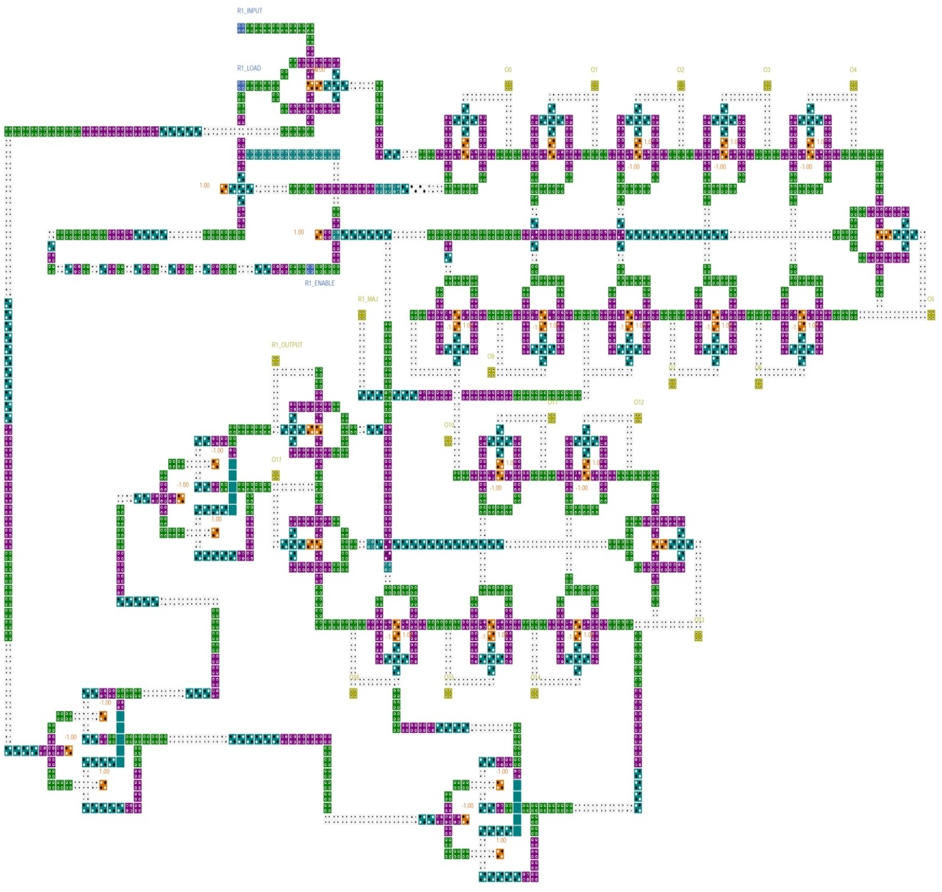 | Figure 6. R1 register |
 | Figure 7. R2 register |
Fig. 8 shows the QCA implementation of the R3 register. This register has 23 memory cells. There are also three XOR gates and a multiplexer in R3 register. The multiplexer is used to select the R3-INPUT when the R3-LOAD is activated. Otherwise, the feedback value is selected. The 10th bit of this register is the clocking bit and the 22nd bit is the output bit. The feedback of this register is computed by 7th, 20th, 21st and 22nd bits which are XORed. When the R3-LOAD input has the logic value of one, the R3-INPUT value will be stored in the 0th bit of R3 register. TheR3-ENABLE input is used to shift the data throughout the R3 register. When this input has the value of one for a clock period, all bits of R3 register, except 0th bit, will store the previous bit's value after five clock periods of latency. The value of 0th bit will be changed after six extra clock periods because its feedback value should be computed by three XOR gates and the XOR gates have a total latency of six clock periods. It means that a shift operation will be accomplished in eleven clock periods. The implementation of the R3 register has a complexity of 1721 cells and an area ofabout 2.664 µm2.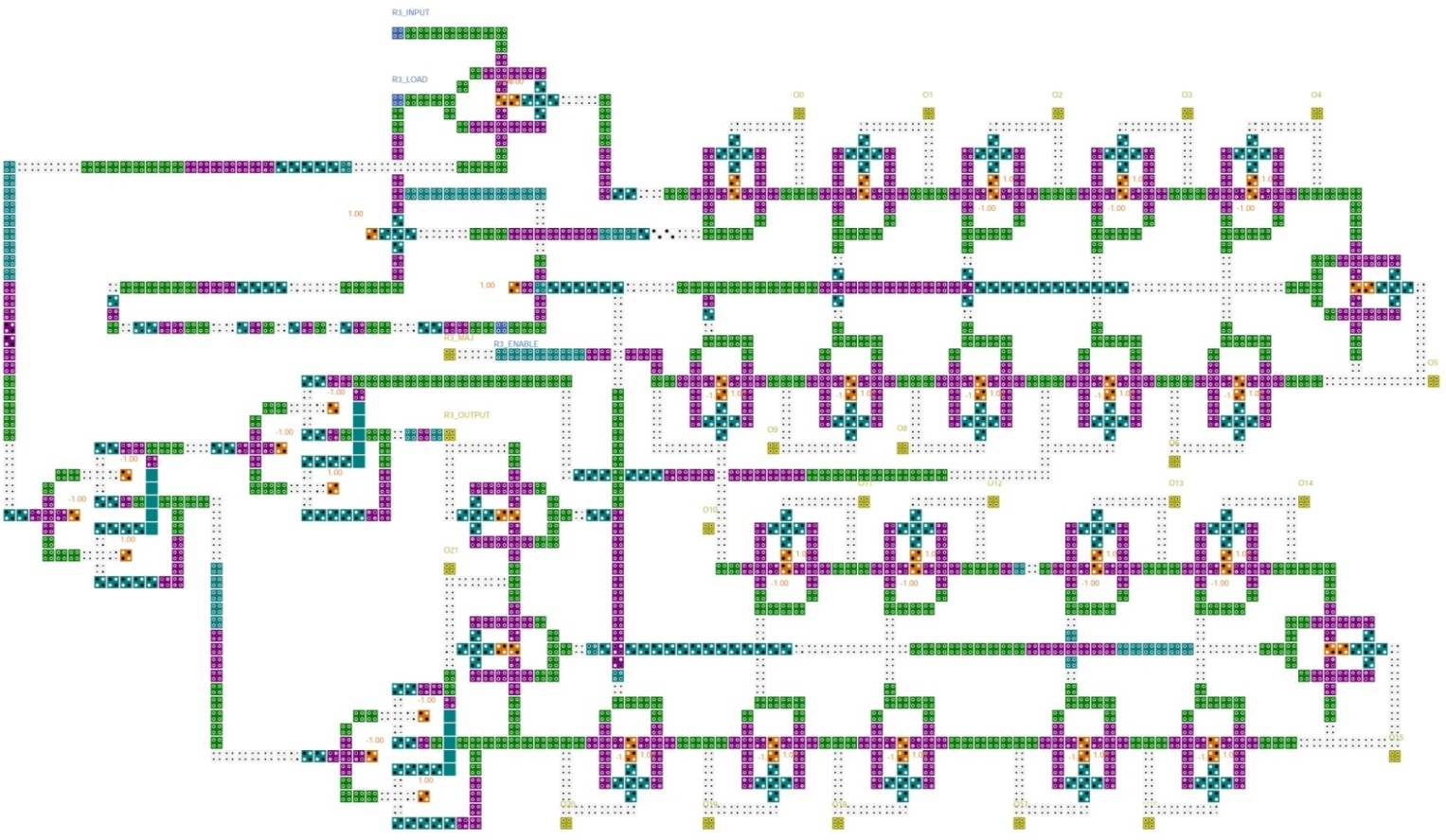 | Figure 8. R3 register |
4. Conclusions
QCA implementation of the A5/1 stream cipher is discussed in this paper. The main blocks of this algorithm which are memory cell, majority function and shift registers, have been implemented separately. The main properties of the implemented modules such as latency, area and complexity are discussed in this paper.
References
| [1] | C. S. Lent, P. D. Tougaw, W. Porod, and G. H. Bernstein, “Quantum Cellular Automata,” Nanotechnology, Vol. 4, No. 1, pp. 49-57, 1993 |
| [2] | M. Briceno, I. Goldberg, D. Wagner, “A pedagogicalimplementation of A5/1,” available online athttp://www.scard.org/gsm/a51.html, 1999 |
| [3] | P. D. Tougaw and C. S. Lent, “Dynamic Behavior of Quantum Cellular Automata,” Journal of Applied Physics, Vol. 80, No. 8, pp. 4722-4735, Oct. 1996 |
| [4] | P. D. Tougaw, C. S. Lent, and W. Porod, “Bistable Saturation in Coupled Quantum-dot Cells,” Journal of Applied Physics, Vol. 74, No. 5, pp. 3558-3565, Sep. 1993 |
| [5] | P.D. Tougaw and C.S. Lent, “Logical Devices Implemented Using Quantum Cellular Automata,” Journal of Applied Physics, Vol. 75, No. 3, pp. 1818-1825, 1994 |
| [6] | M. A. Amiri, S. Mirzakuchaki and M. Mahdavi, “Logic-Based QCA Implementation of a 4×4 S-Box,”' Informacije MIDEM, Vol. 40, No. 3, Sep. 2010 |
| [7] | E. Biham, O. Dunkelman, “Cryptanalysis of the A5/1 GSM Stream Cipher,” Progress in Cryptology, proceedings of Indocrypt’00, Springer-Verlag, pp. 43–51, 2000 |
| [8] | A. Biryukov, A. Shamir, D. Wagner, “Real Time Cryptanalysis of A5/1 on a PC,” Advances in Cryptology, proceedings of Fast Software Encryption’00, Springer-Verlag, pp. 1–18, 2001 |
| [9] | J. Golic, “Cryptanalysis of Alleged A5 Stream Cipher,” Advances in Cryptology, proceedings of Eurocrypt’97, Springer-Verlag, pp. 239–255, 1997 |


 Abstract
 Reference
 Full-Text PDF
 Full-text HTML