Nahid Akter, Suvrajit Roy
Department of CSTE, Noakhali Science & Technology University, Noakhali, Bangladesh
Correspondence to: Nahid Akter, Department of CSTE, Noakhali Science & Technology University, Noakhali, Bangladesh.
| Email: |  |
Copyright © 2019 The Author(s). Published by Scientific & Academic Publishing.
This work is licensed under the Creative Commons Attribution International License (CC BY).
http://creativecommons.org/licenses/by/4.0/

Abstract
This paper focus on the standard and simplified spin on doping process for commercially available mono-crystalline silicon wafers. Commercial mono-crystalline silicon solar cell fabrication uses POCl3 (Phosphorus oxychloride) doping for emitter layer formation. This paper shows the P2O5 spin on dopant source used for emitter layer formation instead of widely used POCl3. Detailed fabrication and characterization results are presented. The pn junction sheet resistivity for doping temperature 875°C for 10 and 20 minutes doping were 60 Ω/sq and 45.6 Ω/sq respectively have been found. A series of other characterization found some correlation between processing steps and quality which can be considered as the contribution of the study.
Keywords:
Spin on doping, Sheet resistivity, Mono crystalline Silicon
Cite this paper: Nahid Akter, Suvrajit Roy, Emitter Layer Formation by Spin on Doping on Mono-Crystalline Silicon Wafer, Microelectronics and Solid State Electronics , Vol. 7 No. 1, 2019, pp. 14-18. doi: 10.5923/j.msse.20190701.02.
1. Introduction
During last decades, the researcher mainly focused on cell efficiency improvement and watt peak cost reduction for crystalline silicon solar cells. Most of PV industries use the standard fabrication process for the reduction of the process cost. The emitter is the most important part and the formation of emitter constitutes a crucial step in the manufacturing of the crystalline silicon solar cells. In case of crystalline silicon solar cell processing, carrier diffusion into p-type or n-type wafer creates emitter formation. For emitter formation the most used technique in photovoltaic industry is POCl3 diffusion in cylindrical quartz tube. Spin-on dopants (SOD) also provide an impurity source for semiconductor junction as well as emitter layer fabrication. Most of the PV industries today use monocrystalline silicon (mono-Si) wafers due to its lower defects compared to other types of wafers. Monocrystalline silicon solar cells are used to maximize the power density in the PV module and to reduce the cost per unit energy. Recent surveys indicate that the wafer cost takes 65% of the total cost. Continuous efforts have been put on multi-wire sawing technology to cut the wafers, make them thinner and reduce material consumption. Wafer of reduced thickness such as 120-150 μm thickness is feasible that needs advanced technology for production but it requires an automated handling process for solar cell fabrication. An automated advanced technology not only increases the efficiency of solar cells but also increases the process cost significantly due to higher equipment and maintenance costs [1, 2, 3].In this work, our goal is to put an intermediate step in between lab-scale fabrication and fully automated commercial facilities or processes. That’s why, the principal motivation is to put stress on the simplicity and the cost effective fabrication process. The use of low cost commercial CZ wafers and the use of SOD instead of doping gas POCl3 can made this work interesting for a low budgeted and industrially compatible fabrication process of solar cells. Eventually, smaller fabrication facilities may be benefited from these comparative studies and get involved in more human resource involved manufacturing around the world to make this technology reachable to all with reduced production cost.
2. Related Works
Lachiq et al. reported a fabrication scheme where the authors used a spin on dopant solution to obtain diffusion with a rapid thermal annealing process in an inert atmosphere. The authors retained the thin (<20 nm) SOD film to serve as a surface passivation layer with further need for an ARC [4].Vikram et al. at University of Virginia in 2010 demonstrated a simplified and single step process on P-type CZ–Si and FZ–Si wafer for photovoltaic device fabrication. Single step process incorporates doping, anti-reflection coating (ARC) and a surface passivation layer. P5O9 was served as the dopant solution for photovoltaic device fabrication [5].
3. Procedure of Research
The starting material used for the fabrication of emitter layer is called wafer. The chosen sample was p-type solar grade mono-crystalline silicon wafer with (100) crystal orientation. The thickness of the wafer is 180±20 µm which was supplied from ReneSola Ltd., China.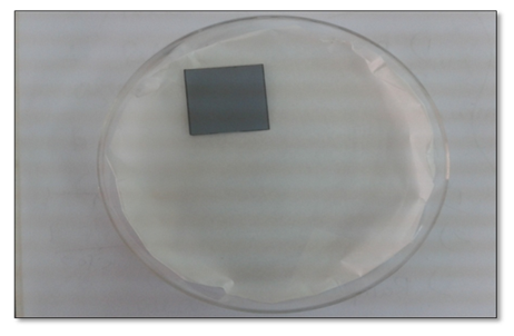 | Figure 1. P-type silicon wafer of 2.2 × 2.2 cm2 |
3.1. Sample Preparation
The first step is the saw damage removal and texturing process for silicon samples. The CZ silicon (solar grade) wafers have micrometer sized surface damages. This layer formed by mechanical saw damage on the surface when it is cut from the ingot. It may contain abraded metal due to sawing and grinding abrasive due to polishing. This surface saw damage on both sides of the sample is needed to be etched off which is called isotropic etching at the beginning of the procedure. Standard RCA process has been used for contaminants free samples. In order to remove the organic and inorganic contaminants from sample surface there are several procedures. Some procedures such as standard piranha solution (H2SO4:H2O2=3:1), standard NaOH or KOH solution (NaOH: H2O=1:10), standard HNO3 and HF solution (HNO3: HF=50:1) can remove the saw damage contaminants [3, 6, 7]. In this work, NaOH aqueous alkali solution was used to remove the saw damage layer. After that wafers were rinsed into HF (2%) for 10 seconds, DI water for 1 minute and then dry with nitrogen blow. For pyramidal growth on the sample surface, Standard RCA process has been used. It is called anisotropic etching the pyramidal surface can reduce the surface reflectance. Few parameters are important for this pyramidal growth process such as chemical concentration, etching time, temperature etc. Several procedures such as standard KOH/IPA solutions, Na2CO3/NaHCO3 solutions, NaOH/carbohydrate solutions can causes anisotropic etching or texturing process. Standard KOH alkaline solution and IPA (iso2 propanol/ isopropyl alcohol) solution has been used in this work [3, 7, 8]. After that textured wafers were rinsed into HF (2%) for 10 seconds, DI water for 1 minute and then dry with nitrogen blow.
3.2. Fabrication of Emitter Layer
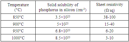
In solar cell fabrication, the emitter is formed by doping process. Doping refers to the addition of specific impurities to a semiconductor to modify its electrical properties. The n-type dopant source comprises of phosphorus compounds along with N2 and O2 gaseous environment is widely used in the thermal diffusion for commercial solar cell fabrication process. Phosphorus compounds react with O2 and create a glass layer on the silicon surface (pre-deposition). The element phosphorus then penetrates into the silicon wafer (drive-in). The solid solubility of phosphorus and the sheet resistivity is temperature dependent and it varies the sheet resistivity of the semiconductor sample.Table 1. Temperature dependent solid solubility of phosphorus and the sheet resistivity for silicon sample [9]
 |
| |
|
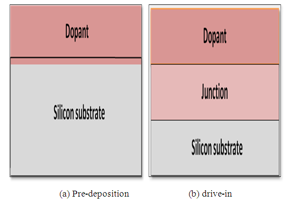 | Figure 2. Structure of layer of thermal diffusion |
This paper focused on spin on doping by P5O9 solution on mono-crystalline silicon wafer. Where, P5O9 is a commercially available phosphorus doped oxide solution. It was supplied from Filmtronics Inc., PA, USA; P5O9 series. This solution is high purity solution where phosphorous can diffuse into silicon with little or no surface damage. The surface concentrations after diffusion depend on the function of concentration of dopant in SiO2 film. The P5O9 solution consists of 10% dopant compound and 5% of SiO2. The concentration of phosphorous in this solution is 2.0×1021 cm-3. This solution contains ethyl alcohol as a solvent and may be thinned with ethanol or isopropanol to modify concentrations. Note that the precise chemical compositions of the SOD solution are not disclosed by the manufacturer.
3.2.1. Spin Coater
The spin on process needs a spin coater to produce a thin layer of dopant solution on single sample substrate [10]. The coater offers a vacuum secured sample holder with capabilities ranging from very small samples to up to 150 mm diameter. The programs of spin coater are easy to set up with up to 99 steps per program with 0 - 2,000 rpm/sec2 acceleration (max speed of 10,000 rpm and a maximum time per step of 6000 seconds). This research had done by a SPS Spin 150 spin coater [5, 10, 11].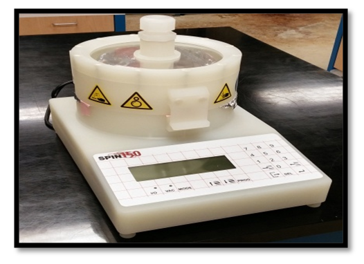 | Figure 3. Front view of SPS Spin 150 spin coater |
3.2.2. Procedure for Film Grown
Two step programming had done by SPS Spin 150 spin coater for P5O9 solution onto the silicon substrate.The initial parameters and solution quantity selection are given below-i. Number of programming steps: 2ii. Dopant solution: 5 ml, where 2.5 ml solution for each steps.iii. Wafer size 2.2 × 2.2 cm2iv. Chosen rpm 1000v. Time 80 secondsAt first the wafer was placed on vacuum secured sample holder of the tool. In the first step, the target was to reach 500 rpm by 10 seconds with an acceleration of 50 R/sec2 and hold it for 5 seconds. As soon as it reached to 500 rpm, put 2.5 ml of P5O9 solution by a dropper/ pipette onto the wafer.In the 2nd step, the target was to reach 1000 rpm from 500 rpm by 50 seconds with an acceleration of 10 R/sec2 and hold it for 1000 rpm for 15 seconds. As soon as it reached to 1000 rpm, put the rest 2.5 ml of P5O9 solution by the same procedure onto the wafer. Figure 3 shows the two step program settings on SPS Spin 150 spin coater.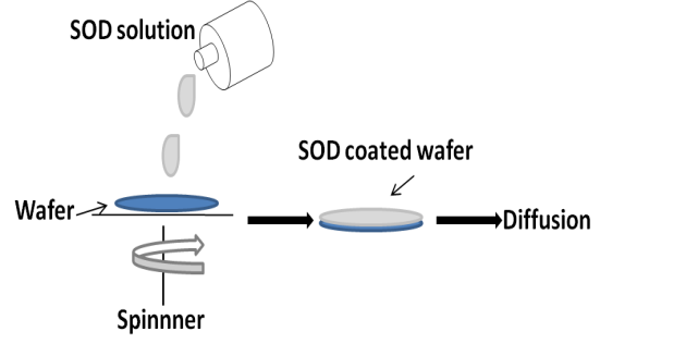 | Figure 4. Spin on doping system |
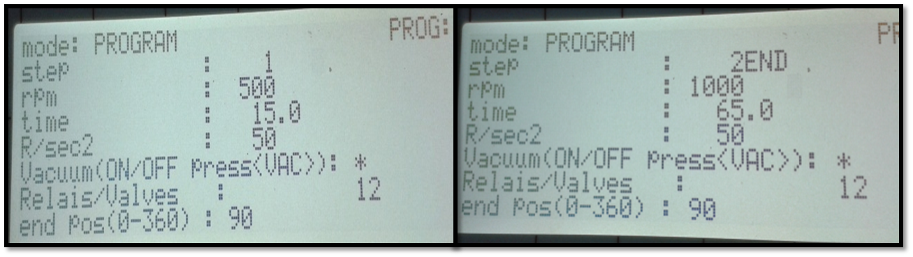 | Figure 5. Two step program on SPS Spin 150 spin coater |
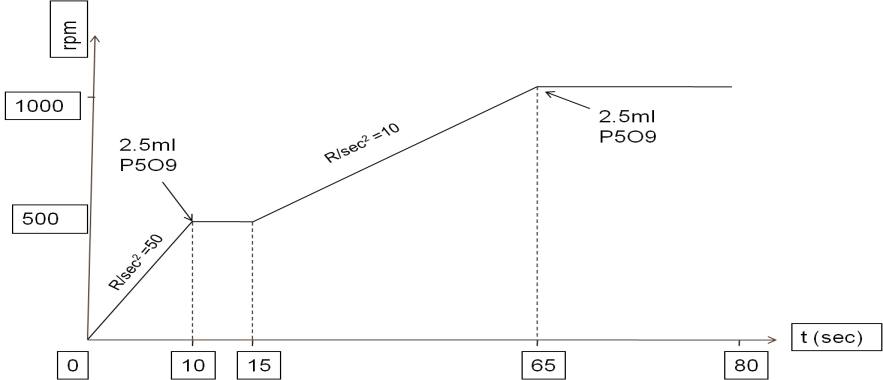 | Figure 6. rpm versus time profile |
3.2.3. Baking
After that the wafer was heated to 200°C for 10 minutes. The hot plate from Fisher Scientific™ Isotemp™ with Ceramic Tops was used in this purpose. The liquid solvents (ethyl alcohol) were evaporated and the phosphorus dopant solution forms a solid film.
3.2.4. Diffusion by Annealing Furnace
After that the wafers were heated at 875°C in the diffusion furnace with N2:O2 [3:1] environment for 10-20 minutes where phosphorus diffuses through the wafers [5, 12]. In this research, the rapid thermal annealing from MTI Corporation OTF-1200 X was used to diffuse the phosphorus into the silicon substrate. The diffusion was carried out at 875°C with the N2 environment. Two measurements have taken for 10 minutes and 20 minutes diffusion. The chosen purified N2 flow rate was 30 sccm. 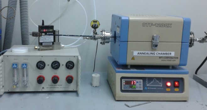 | Figure 7. Diffusion Process inside the annealing chamber |
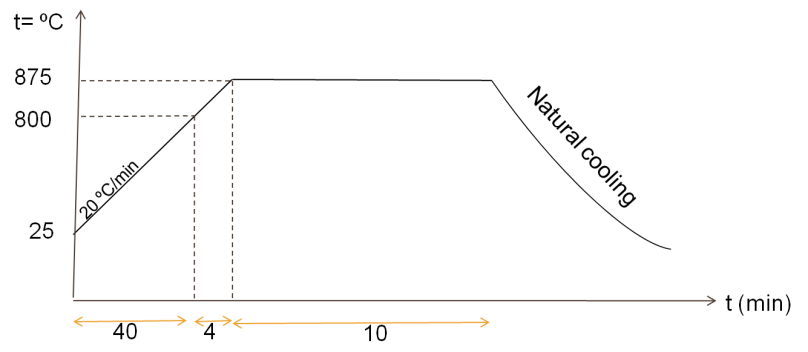 | Figure 8. Time versus annealing temperature profile |
3.2.5. Edge Isolation
The Phosphorus doped layer covers the entire surface including edges. It is important to disconnect the front emitter from the back contact through etching the edges of the sample. Several processes are involved such as chemical etching, plasma etching, laser cutting, mechanical sawing, grinding with sand paper, single side etching etc. In this research single side etching and laser cutting techniques were used. For the single side etching, HF/HNO3 acid barrier paste was used. It was carried out by screen printing process. Samples were heated by 120°C for 10 minutes by oven. Advantages of single side etching are preserving the active cell area, lower parasitic loss, higher FF compared to laser isolation process [3].
4. Results
4.1. Optical Microscopy
Optical microscope from Radiation Technology Company Ltd. (Taiwan) for optical imaging was used as a primary tool for viewing surface morphology of raw, cleaned and textured silicon wafer. 2D images of silicon surface was taken using bright field microscopy where light falls vertically on the top surface of the sample. Bright field microscopy is useful to observe the sample surface topography. Figure 9 shows the 2D camera image from the reflectometer.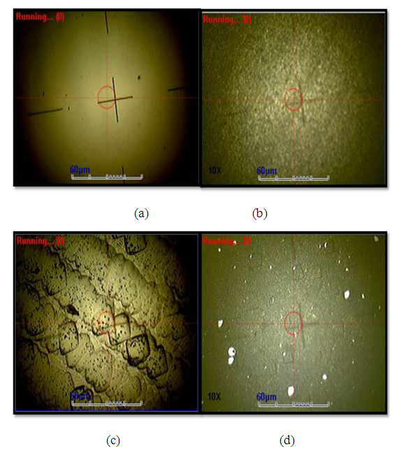 | Figure 9. 2D optical images with magnification 10X (a) SiCr reference sample for calibration (b) raw silicon wafer (c) cleaned silicon wafer (d) textured silicon wafer |
4.2. Spectral Reflectance Measurement
The light reflectance was also measured by spectral reflectance measurement (SRM) system. It is a simple, low cost, computer-controlled, normal light incidence measurement system. It is consist of a stepper motor driven mini monochromator where the spectral range is 400-1200nm. Unlike the spectroscopic reflectometer, the incident light is not focused in a point. A spread incident light of almost one inch diameter was incident on the sample. Light comes from the exit slit of the monochromator that is guided to the wafer at near normal incidence. Stepper motor is used to vary monochromator output wavelength. A light chopper is placed at the exit slit of the monochromator to provide reference signal to the lock-in to ensure all the stray light is rejected by the system and enhance system sensitivity from nano volt to mV range. Surface reflection as a function of wavelength is determined by measuring photodetector response. In order to determine spectral response, the sample at first placed on vacuum chunk with top and bottom contact for probing. A LabVIEW interface is used for data acquisition.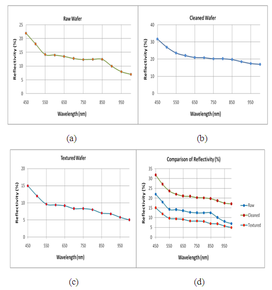 | Figure 10. Percentage of Reflectivity versus wavelength graph (a) Reflectivity (%) for raw silicon wafer (b) Reflectivity (%) for cleaned silicon wafer (c) Reflectivity (%) for textured silicon wafer (d) Comparison of reflectivity (%) shows the reduced reflection for the pyramidal growth textured sample |
4.3. Resistivity Measurement by Four Point Probe
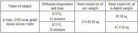
The four point probe apparatus is one of the standard apparatus for the measurement of resistivity of semiconductors. If the sample is in the form of a thin wafer or the form of a thin semiconductor material deposited on a substrate then it is also useful for the measurement. Table 2. Measurement of sheet resistivity for raw and n-doped sample using four point probe
 |
| |
|
5. Conclusions
In this study, one key research issue have been identified regarding to low budgeted manual fabrication process. The issue is to reducing the expensive and time consuming processing steps. Time consuming processing steps incorporates phosphorus diffusion, anti-reflection coating (ARC) and a surface passivation. These processing steps are overcome by the single step of emitter layer formation. From the identified key issue, two research objectives have been outlined. The first objective is to explore a simplified thermal diffusion process by spin on dopant P5O9 solution on commercial silicon wafer. The procedure carried out at 875°C. The P5O9 spin on dopant solution mainly comprises of P2O5 and dissolved SiO2 in organic solvents. That’s why the spin on dopant film was retained to serve as an ARC and surface passivation layer after doping. The achieved conversion efficiency was 4-5% which proves viability of the approach. However, the relatively lower efficiency was mainly caused by the manual in hand complete procedure without any optimization of the process and the use of low cost wafers. The second objective is to explore the characterization after each step of fabrication. Future prospect would be the enhancement of the efficiency improvement, fabrication under standard clean room environment, measurement of ARC thickness as well as passivated layer characterization etc. Finally, to improve the quality, portable desiccated and sealable chamber, need to be ensured for sample handling and transferring from one system to another without exposure to the atmosphere. It can be conclude by minimize the bridging gap between small scale laboratory solar cells with the commercial prototypes producing extensive knowledge in each processing steps.
ACKNOWLEDGEMENTS
The author would like to thank at the staff of Solar Energy Technology Research Laboratory, Institute of Fuel Research and Development, Bangladesh Council of Scientific and Industrial Research and Solar Cell Fabrication Laboratory, Institute of Electronics, Atomic Energy Research Establishment, Savar, Dhaka, Bangladesh for the technical support in this work.
References
| [1] | H. Ghembaza, A. Zerga, R, Saim: Efficiency Improvement of Crystalline Silicon Solar Cells by Optimizing the Doping Profile of POCl3 Diffusion. International Journal of Scientific & Technology, vol 3, no. 1, January 2014 (ISSN 2277-8616). |
| [2] | https://www.filmtronics.com/capabilities/products/diffusants. |
| [3] | M. Al-Amin and A. Assi, Efficiency improvement of crystalline silicon solar cells, Materials and Processes for Energy: Communicating Current Research and Technological Developments (2013), 22-31. Energy materials. Web. 17 Nov. 2014. |
| [4] | A. Lachiq, A. Slaoui, L. Georgopoulos, L. Ventura, R. Monna, J.C. Muller, Simultaneous dopant diffusion and surface passivation in a single rapid thermal cycle, Progress in Photovoltaics: Research and Applications 4 (1996) 329–339. |
| [5] | V. V. Iyengar, B. K. Nayakk and M.C. Gupta, Silicon PV devices based on a single step for doping, anti-reflection and surface passivation, Solar Energy Materials & Solar Cells 94 (2010), 2205-2211. |
| [6] | S. M. Iftiquar, Y. Lee, M. Ju, N. Balaji, S. K. Dhungel and J. Yi. (2012). Fabrication of crystalline silicon solar cell with emitter diffusion, SiNx surface passivation and screen printing of electrode, Photodiodes - From Fundamentals to Applications, Dr. Ilgu Yun (Ed.), ISBN: 978-953-51-0895-5, InTech, DOI: 10.5772/51065. |
| [7] | C. Sethi, V. K. Anand, K. Walia, S.C. Sood, Optimization of surface reflectance for alkaline textured monocrystalline silicon solar cell, International journal of computing science and communication technologies, vol 5, no. 1, July 2012 (ISSN 0974-3375). |
| [8] | W. Sparber, O. Schultz, D. Brio, G. Emanuel, R. Preu, A. Poddy, D. Borchert, Comparision of texturing methods for monocrystalline silicon solar cells using KOH and Na2CO3, WCPEC-3, Osaka, May 11-18. |
| [9] | https://0x9.me/V1RZjq. |
| [10] | http://www.vtpup.cz/common/manual/PrF_RCPTM_SPS_Spin150_datasheet_EN.pdf. |
| [11] | https://cse.wwu.edu/amsec/sps-spin-150-spin-coater. |
| [12] | Lee Y-Y, Ho W-J, Syu J-K, Lai Q-R, Yu C-M: 17.9% Efficiency Silicon Solar Cells by Using Spin-on Films Processes. In PIERS, Progress in Electromagnetics Research Symposium. Suzhou, China; 2011:780.Google Scholar. |

 Abstract
 Reference
 Full-Text PDF
 Full-text HTML