-
Paper Information
- Paper Submission
-
Journal Information
- About This Journal
- Editorial Board
- Current Issue
- Archive
- Author Guidelines
- Contact Us
Microelectronics and Solid State Electronics
p-ISSN: 2324-643X e-ISSN: 2324-6456
2019; 7(1): 1-13
doi:10.5923/j.msse.20190701.01

In Search of the “Forever” Continued Scaling of CMOS Performance by Means of a Novel Monolithic 3-Dimensional System-on-top-of-System Approach
 Abstract
 Reference
 Full-Text PDF
 Full-text HTML
Ahmad Houssam Tarakji1, Nirmal Chaudhary2
1Device Organization Unit, Solidi Technologies, Sacramento, California, United States of America
2Consultant Engineer, Leesburg, Virginia, United States of America
Correspondence to: Ahmad Houssam Tarakji, Device Organization Unit, Solidi Technologies, Sacramento, California, United States of America.
| Email: |  |
Copyright © 2019 The Author(s). Published by Scientific & Academic Publishing.
This work is licensed under the Creative Commons Attribution International License (CC BY).
http://creativecommons.org/licenses/by/4.0/

We demonstrate the potential of monolithic Three-Dimensional (3D) Integrated-Circuits (IC’s) to enhance the performance and the power-efficiency of next generation Central Processing Units (CPU’s) and System On Chips (SOC’s). We demonstrate with established simulations that derived from design-rules set by the International Technology Roadmap for Semiconductors (ITRS) that it is feasible to clock these next generation monolithic 3D architectures for CPU’s and SOC’s at extreme frequencies above 30GHz provided the excessive heat generated from such ultra-fast switching is effectively managed. Simulations also specifically demonstrated that it is feasible to clock these systems at frequencies close to 30GHz without necessitating or requiring further heat management beyond what is presently adopted in today’s conventional two-dimensional (2D) Integrated-Circuits (IC’s). This is possible because the inline interconnects in our novel monolithic 3D architectures trim the dynamic power losses by up to four times relative to today’s conventional 2D IC’s. Additionally, the Fully-Depleted Silicon-On-Insulator MOS in our 3D monolithic architectures utilizes a software-controlled transistor back-biasing that dynamically cuts the transistors standby power by more than two orders of magnitude when transistors are off. The substantial reduction in standby power achieved through this approach will enable transistors to satisfy even higher dynamic losses with faster clocking without increasing the overall self-heating. This approach to monolithic 3D integration will enable the continuation of Moore’s law and is manufacturable in standard CMOS-like processes that rely on none other than “good old” Silicon and copper interconnects that are still among the very few materials to date that possess the flexibility to manufacture and produce large-scale integrated electronics in high-volumes. These novel monolithic 3D architectures for next generation CPU’s and SOC’s can dramatically trim the power consumptions in laptops, smartphones, servers, and from the computation intensive data mining and the data centres’ around the globe.
Keywords: Monolithic 3D, CMOS, High performance computing
Cite this paper: Ahmad Houssam Tarakji, Nirmal Chaudhary, In Search of the “Forever” Continued Scaling of CMOS Performance by Means of a Novel Monolithic 3-Dimensional System-on-top-of-System Approach, Microelectronics and Solid State Electronics , Vol. 7 No. 1, 2019, pp. 1-13. doi: 10.5923/j.msse.20190701.01.
Article Outline
1. Introduction
- After the 90nm CMOS technology node RC-delays from inline interconnects have increased significantly relative to transistor intrinsic delay to become a major bottleneck in improving the performance of advanced Integrated-Circuits (IC’s) [1]. Increasing the switching-speed of CMOS alone is no longer increasing the overall speed in today’s Central Processing Units (CPU’s) due to these RC-delays from interconnects.CMOS device scaling from one process technology to the next has compelled the cross-section areas of interconnects (Ac), the spacing’s between them (S’s) and the heights of vertical spacing between them (H’s) to keep shrinking correspondingly in order to accommodate the on-chip integration of an increasing number of smaller transistors. This has prompted the resistance per unit-length in local and global interconnects to increase continuously and steadily with scaling. Therefore, although the length of interconnects between transistors and circuit-modules has been reducing from one process technology to the next, their line resistance has been continuously increasing. This is because the decrease of product
 outweighs the corresponding decrease in interconnects line length that has been reducing by the same factor as W and T (~ 0.7×). W is the width of an interconnect line and T is its vertical height or thickness. The line capacitance per unit-length for interconnects on the other hand has remained virtually unchanged because the W’s, T’s, S’s and H’s have been reducing proportionally with this scaling by the same factor (~ 0.7×) [2]. Consequently, the RC-delays from interconnects have been increasing steadily with the continuing progress of CMOS from one node to the next. Furthermore, the on-going steady decrease of Ac has started to result in far more pronounced increase in the RC-delays from interconnects such that any performance enhancement to frontend is being negated nowadays by these RC-delays (the backend).Additionally, this increase in electric resistance coupled with the continuing increase of the transistors standby current (from continuous decrease of the transistors Gate pitch) and the continuing increase of dynamic losses due to continuous increase in clock frequency, have pushed all of today’s CPU’s closest to their thermal limits (referred to in technical literatures as: The “Power-wall”).The trend followed today to circumvent these dilemmas (RC-delays and Power-wall) has been to divide the work that was once done in a single processor among several processing cores (or CPU-cores) that are monolithically integrated together. The merit in this approach is that it exploits computational parallelism to counter the speed impediment due to interconnect. It also dissipates the same amount of heat over a wider surface area. So, although the chip uses more power, the overall heat density per surface-area is reduced. One hurdle in this approach however is that it still does not substantially speed up the computations of sequential arithmetic’s, something that is critically needed nowadays for more rapid and accurate computations of massive and complex analytics such those encountered in computationally intensive neural-networks and artificial-intelligence systems. Another hurdle in the conventional approach is the substantial increase in the length of certain global interconnects that are required to inter-bridge the many CPU-cores. These interconnects have recently started exceeding 10,000µm, adding even more delays for the cores to synchronize their outputs. Additionally, the active and standby powers are starting to increase drastically with the transistor-count and no longer with the computing performance. This has already started to prevent transistors from being switched or powered on simultaneously (referred to in today’s technical literatures as: “Dark Silicon”). Pursuing this brute-force approach of continuously multi-coring and increasing Cache size will ultimately lead to future processors crashing again into the “Power wall”. Lastly, the end of Moore’s law as it relates to scaling means that the CMOS Gate lengths will not shrink below 3nm [3].Although overall computer performance can be impeded from slower communication between computer main memory (DRAM) and the processor (CPU), once the data is fetched into Cache memory the computing speed is then impeded from inline interconnects in processor because Cache memory is integrated monolithically within a processor. As Cache size grew substantially larger over the years encompassing tens of Mega-Bytes, the speed impediment from inline interconnects in processor has become more pertinent and is starting to more frequently impact the overall speed of a computer. Nulling or substantially suppressing this speed impediment is therefore key to enhancing the overall computer performance. While the United States Defence Advanced Research Projects Agency (DARPA) is presently exploring “Photonics in the Package for Extreme Scalability” (PIPES) to null or suppress delays and scale-down the dimensions in packaged electronics, similar methods that consider optics as a substitute for inline interconnects in processors cannot apply because the dimensions of inline interconnects in today’s processors (CPU’s) are order(s) of magnitude smaller than any optic wavelength (these are even smaller than wavelength for Extreme Ultra-Violet). PIPES may be successful at enhancing communication between the computer main memory and CPU.In this work we demonstrate a new monolithic 3-dimentional (3D) architecture for next generation CPU’s and SOC’s that effectively suppresses RC-delays and the dynamic power losses from interconnect. It methodically inter-wires the system-blocks of CPU’s and SOC’s with far shorter interconnects (in nanoscale range) using a 3D approach as opposed to the long bulky global interconnects used in today’s conventional 2D IC’s. Our simulations have demonstrated substantial suppression of both the RC-delays and the dynamic losses, thus, enabling a far higher clocking speed. This 3D architecture also employs a double-sided Fully Depleted Silicon on Insulator (FD-SOI) CMOS with software-programmable secondary Gates (back-Gates) that cut the standby power by more than 2 orders of magnitude when transistors are Off. This suppression of standby power enables the transistors to satisfy an even faster clocking without increasing the overall self-heating.Through these effective suppressions of dynamic and standby powers, and the RC-delays from interconnects, future performance enhancements to the CMOS frontend can start contributing again to the speed and performance of next-generation CPU’s and SOC’s.
2. RC-Delays and the “Power-Wall” Dilemmas in Today’s CPU’s
2.1. Delay Model and the Simulation of Past and Current Trends
2.1.1. The Interconnect Model
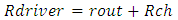
- We estimated the time propagation delay of an electric signal due to interconnects by modeling its equivalent time transient response using a lumped -shaped interconnect circuit model. When inductive effects are suppressed this time transient response follows an analytic expression for the Elmore time delay as described in [4]. According to [4], this delay is estimated at any given node in a circuit-tree comprising a plurality of “Cauer” RC ladders [5] by multiplying each resistor along the signal propagation path before that node by all the line-to-ground capacitances that are downstream from this resistor. Therefore, for the circuit of “Figure 1” that depicts, with -shaped lumped circuit model, an interconnect line that connects from its beginning and from its terminated end to plurality of CMOS inverters in parallel, the Elmore time delay for the voltage rise
 at this interconnect line termination due to an applied unit step voltage V to this line is
  | (1) |
 are all the n paralleled line-to-ground capacitances that the terminated interconnect line sees. It models the equivalent Gate input capacitances of the many paralleled CMOS inverters that branch-out from this interconnect line termination at the node v(t). Similarly,
  are all the m line-to-ground paralleled capacitances at the beginning of same interconnect line. It models the equivalent Gate input capacitances of the many paralleled CMOS inverters that branch-out from this interconnect line beginning at the node vdr(t). Such representation of an interconnect line that feeds several CMOS-systems branching-out in parallel from its terminated end and from its beginning is illustrated in the schematic of “Figure 1”.
 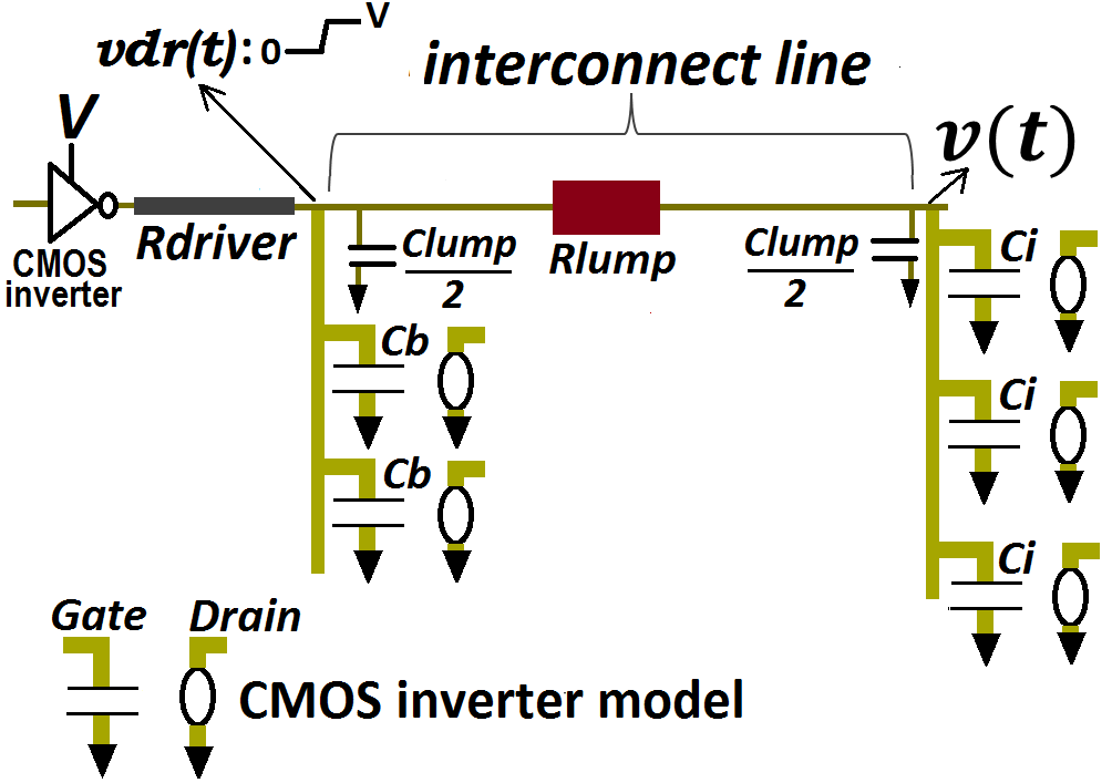 | Figure 1. Schematic illustrating a lumped -shaped model for an interconnect line that is connected from its terminated end to the Gated-input of 3 CMOS-systems in parallel (n = 3), and from its beginning to Gated-input of 2 CMOS-systems- in parallel (m = 2) |
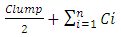 . We refer throughout this work to the summation:
  as: Celmor (the Elmore time delay capacitance). It is the total equivalent load capacitance at the interconnect line termination that impedes the signal rise in global interconnects.An accurate physical model for inline interconnects is utilized from [6]. This model combines in one capacitance (Cdist) the distributed capacitive effect from three distinct components that are: the Plate capacitance
  , the edge capacitance
  , and the fringe capacitance
  . It models the capacitance of any interconnect line that conducts between two other interconnect lines, one that is in parallel above it and one that is also in parallel below it, or between one interconnect-line in parallel above it and a Silicon plane in parallel below it. The per-unit length expression for this distributed line capacitance is
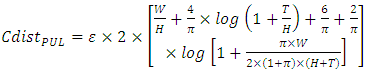 | (2) |
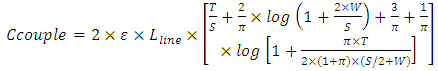
 couples simultaneously to either the grounded Silicon plane or a grounded interconnect line below it and to another grounded interconnect line right above it. In this scenario the total line capacitance becomes
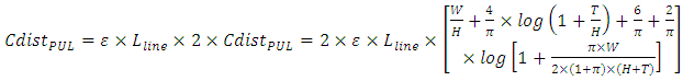 | (3) |
 is the dielectric constant for the inline dielectric between the interconnects. Model assumed the conducting interconnects and those in parallel to it follow simple straight path throughout the length of the interconnect that is conducting:
  . “Figure 2” shows a cartoon schematic depicting this capacitive model of interconnects.
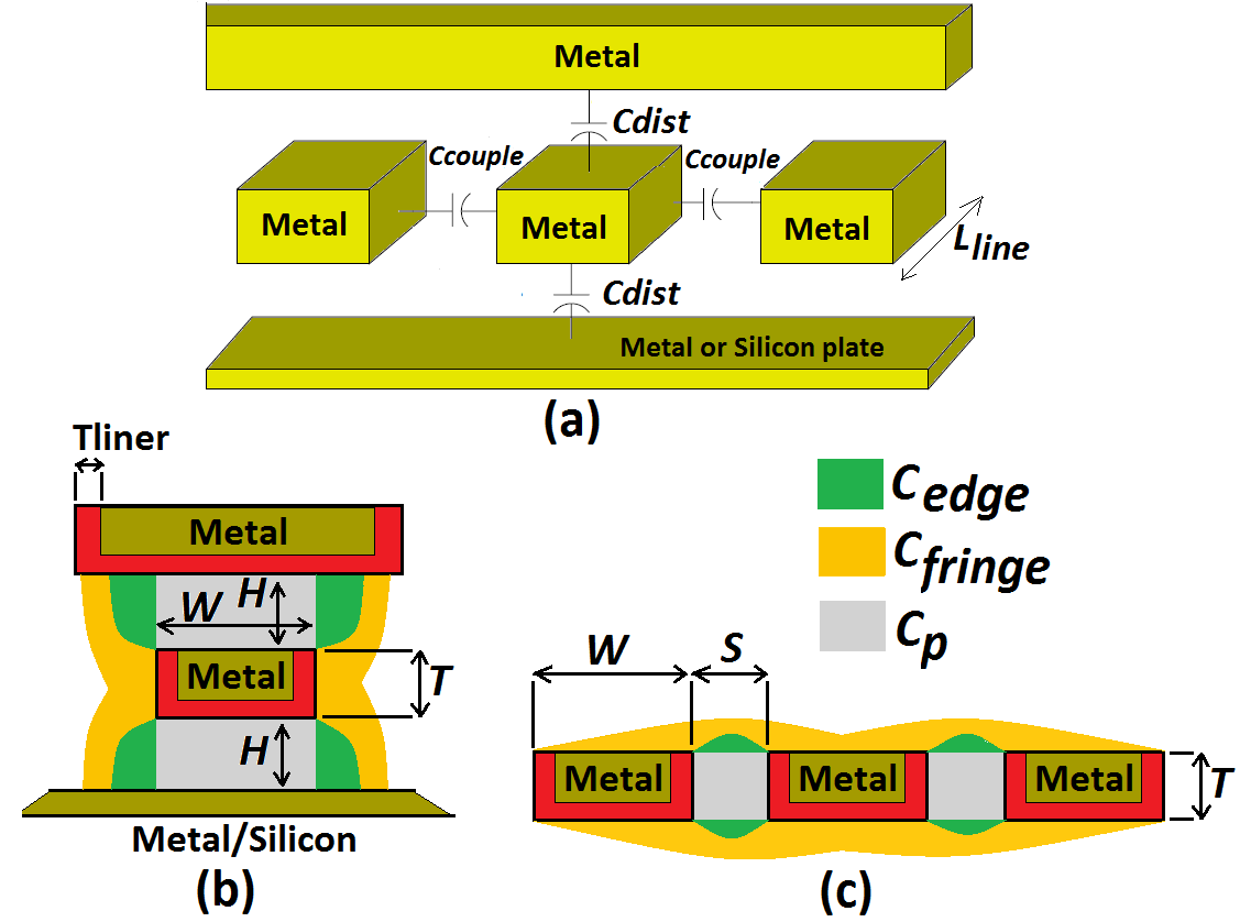 | Figure 2. (a) Interconnects model. (b) Model for edge and fringe capacitance effects in Cdist. (c) Model for edge and fringe capacitance effects in Ccouple |
 | (4) |
 | (5) |
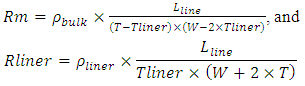
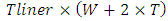 models the effective equivalent area for the Liner, and Tliner is the thickness of the Liner film.Model for the distributed interconnect line inductance is taken from [7]. Its expression is
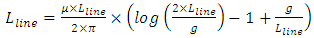 | (6) |
 Inductive effects become suppressed when damping factor ξ is larger than unity. In converting the -shaped lumped circuit model of an interconnect line to its equivalent L-shaped model, an estimate of ξ for the circuit in “Figure 1” is
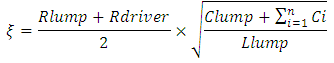 Since
Since  is typically large because an interconnect line always drives or connects to plurality of paralleled inverters, ξ is almost always greater than unity. This is especially true in global interconnects that additionally have large values for their Rlump and Clump.From the
  lumped circuit model, the time domain unit step transient rise at an interconnect line termination is therefore
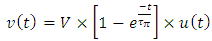 wherein u(t) is the unit step function at time t=0. The unit step transient fall at same interconnect line termination when the discharging path has same resistance Rdriver is:
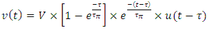
 is the unit step function at time
2.1.2. Simulations of Past and Current Trends
- Simulations of past and current trends for interconnect delays followed design-rules in 32nm and 22nm nodes as these were specified in the 2017 International Technology Roadmap for Semiconductors (ITRS) [8]. Additional design-rules for 14nm and 10nm nodes were interpolated following same ITRS scaling trend.Assumptions used in simulations followed published work based on 130nm node [9] in which it was specifically reported that the mean (or averaged) length
 for global interconnects is the long length that inter-wired most large networks or system blocks in a CPU-core. We consequently carried simulations on all 32nm, 22nm, 14nm, and 10nm nodes considering the delay that propagates through
  is what actually dominates the overall speed in a CPU-core. Our simulations neglected the vertical paths of conduction from Contacts to the global interconnect layer (these are sufficiently small compared to
  ). It was reported in [10] that, when the
  has same W and T values and same electric metal resistivity as the maximum length for global interconnection that inter-wires the large system blocks that are farthest apart in a CPU-core (
 ) (that is, it lies in the same global interconnect layer), this
  is about an order of magnitude (~13x) lower than this
  . An expression for this
  from [10] is
 | (7) |
 is therefore
 | (8) |
 Die areas for CPU-cores of other process nodes were all calculated for same transistor-count equaling 544 Million transistors and by following the same published trend in [12]. All these die areas were calculated to be reducing with smaller nodes and this is consistent with all Intel’s latest products. The higher transistor-count in these products was rather coming from the monolithic integration of more cores and not from larger surface area per one CPU-core.Lengths for the local Metal-1 interconnects were set in simulations two orders of magnitude lower than
  . This follows published data on 130nm process node wherein the range between the averaged length for “local” metal-1 interconnects
  and
and  was reported approximately two orders of magnitude [9]. We assumed in our simulations that a same range holds for all the process nodes. This is because while
  and
and  have been shifting with each subsequent technology node, they both were shifting by roughly same factor. The design-rules and other parametric constants used in simulations are all shown in Table 1.
|
 | (9) |
 ). In considering the Elmore time delay
  as our measure to gage the delay due to an interconnect line, “Figure 3” demonstrates maximum clock frequencies (Freq) hindered from interconnect delay equaling:
  . These are close to the highest frequencies in today’s fastest CPU‘s when these are over-clocked. Because transistors that supply global interconnects are typically large-periphery high current devices, a 16mA CMOS (having its n-MOSFET current matched to that of its p-MOSFET) was considered in the simulations of “Figure 3” which while neglecting rout and for
 With a current density between 1.75mA-1.95mA/µm this CMOS has a total Gate width close to 8-9µm. The subplot of “Figure 3” shows that although the per-unit length interconnect line capacitance
  remained virtually constant with the continuing downscaling of the interconnect pitch from one technology node to the next, the per-unit length of interconnect line resistance was on the other hand increasing drastically. The linear decrease of the total interconnect line capacitance (Clump) with continuing decrease of
  is therefore countered by this pronounced increase of the interconnect line resistance (Rlump). These findings are consistent with what was reported in [2] for inline metal-1 interconnects, and that is exactly what has caused the clock speed in CPU’s to cease from increasing any further after the 90nm CMOS technology node.
 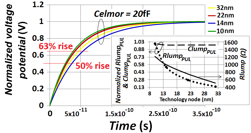 | Figure 3. Simulated time delay through global interconnects 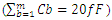 . Subplot: Resistances (Rlump) of global interconnects for different technology nodes and their per-unit length values . Subplot: Resistances (Rlump) of global interconnects for different technology nodes and their per-unit length values  ; and the per-unit length values of parasitic capacitances of global interconnects ; and the per-unit length values of parasitic capacitances of global interconnects  . (The peak value for . (The peak value for  is 11.6Ω/µm, and the peak value for is 11.6Ω/µm, and the peak value for  is 0.33fF/µm) is 0.33fF/µm) |
 rise in all nodes for large Celmor equaling 20fF and
  was simulated around 1.7ps. This is close to 30x lower than the simulated time delay caused by global interconnects for same Celmor. By re-simulating same time delays with lower value of Celmor equaling 2fF this
  rise reduced to 0.3ps. “Figure 5” shows the calculated ξ parameters in local metal-1 and in global interconnects for all the simulated nodes. As seen all values for ξ are above unity. This validates the assumption made in equation (1). Also shown in “figure 5” are the values of the parasitic inductances as these were calculated from equation (6) and used in the ξ calculations. Values of Clump used in the same calculations of ξ were those from “Figure 3” and “Figure 4” after they were normalized relative to their
  .
.  | Figure 4. Simulated time delay through local metal-1 interconnects  . Subplot: Resistances (Rlump) of metal-1 interconnects for different technology nodes and their per-unit length values . Subplot: Resistances (Rlump) of metal-1 interconnects for different technology nodes and their per-unit length values  ; and the per-unit length values of parasitic capacitances of metal-1 interconnects ; and the per-unit length values of parasitic capacitances of metal-1 interconnects  . (The peak value for . (The peak value for  is 44Ω/µm, and the peak value for is 44Ω/µm, and the peak value for  is 0.32fF/µm) is 0.32fF/µm) |
 being far higher than the lengths of metal-1 interconnects
  and of those of other local inline interconnect layers.
 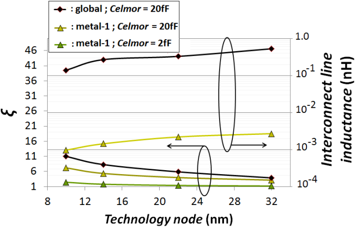 | Figure 5. Simulated values of ξ and the calculated line inductance magnitudes |
 for same global and metal-1 interconnects. It also demonstrates how these delays due to interconnects compare to the intrinsic CMOS frontend delay in far smaller CMOS devices that all have a Gate width WG equaling 0.5µm, and just one 20fF capacitor C connected straight to their output. The intrinsic CMOS frontend delay was estimated following equation (1) after setting all the interconnect line parameters and
  to 0, and setting the
  .
.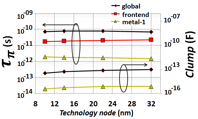 | Figure 6. Simulated values of interconnect line capacitances and 63% delay due to global and metal-1 interconnect lines that are driven with large-periphery CMOS  ; and the delay due to the intrinsic frontend performance of a smaller periphery CMOS ; and the delay due to the intrinsic frontend performance of a smaller periphery CMOS  |
 Values for V and Ion corresponding to 32nm and to 22nm nodes were taken from [8, 12], and the same scaling trend from these references was utilized to interpolate additional magnitudes for V and Ion corresponding to 14nm and 10nm nodes. These values for V in 32nm, 22nm, 14nm and 10nm were correspondingly: 0.95V, 0.9V, 0.85V and 0.8V, and for Ion values were correspondingly 1.75mA/µm, 1.8mA/µm, 1.85mA/µm and 1.9mA/µm.Most apparently the
  from global interconnects driven by large-periphery CMOS (which
  ) are in all nodes close to an order of magnitude higher than the intrinsic CMOS frontend delay in far smaller device peripheries (which
  ). This demonstrates that even CMOS devices supplying far smaller currents (0.88 - 0.95mA) are far faster when they do not drive a global interconnect line. This effect from global interconnect is negating in the first place the performance enhancement from the frontend.
2.2. The Power-wall Setback
2.2.1. Dynamic Power Dissipation
- Higher dynamic power dissipates in global interconnects because these carry a far higher capacitive load. Their capacitive load is two folds: 1- Lumped equivalent capacitance resulting from much longer interconnects (Clump), and 2- added capacitive loading from the many system blocks that are connected to same global interconnect line. This explains the thermal simulations in [8] that clearly demonstrated a far more heating at distances that are furthest from the Silicon. This is simply because global interconnects run through these distances.The amount of energy that charges the entire length of an interconnect line is
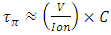
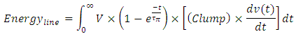 The Elmore time delay
  was considered in the above equation because this is the corresponding time constant for charging the interconnect line in its entirety. After substituting
 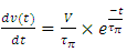 in the above equation, integrating that equation, and evaluating it for its limits we get
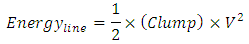 Because the interconnect line of “Figure 1” carries capacitive loads from its beginning and from its terminated end an additional energy also stores in these capacitive loads as the line charges. This energy is
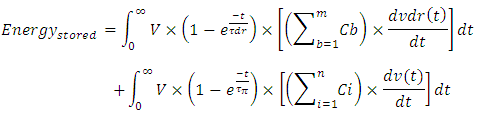 wherein
  is the Elmore time delay at the beginning of this interconnect line. Its expression from [4] is
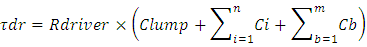 After substituting
 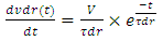 , and
, and 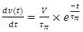 in the equation for the
  , integrating that equation, and evaluating it for its limits we get
  Therefore, the total energy that stores throughout this interconnect line is
 During the discharging transition when n-MOSFET switches On and P-MOSFET switches Off, this total energy dissipates in interconnect line and in Rdriver. Same amount of energy also dissipates in interconnect line and in Rdriver during the charging transition when p-MOSFET switches On and n-MOSFET switches Off. Total power that dissipates in interconnects and in Rdriver during an entire clock cycle while the CMOS inverter switches is therefore
 | (10) |
2.2.2. CMOS Standby Power
- Equation modeling standby leakage current follows the model described in [14]. The corresponding equation is
 | (11) |
 is the thickness of the induced residual charge in the surface channel of the MOSFET, Ar (10A/(cm2.K2)) is the Richardson’s constant and T is the temperature (300⁰K). The corresponding short-channel device threshold voltage (VT) can follow same model described in [14] that accounts for the effects from back-Gate biasing. When frontend utilizes double-sided FD-SOI CMOS incorporating secondary Gates (back-Gates) on both n-MOSFETs and p-MOSFET, a substantial impact on the standby power suppression can be achieved as the biasing of these back-Gates does significantly shift the VT on these transistors when these are turned Off. Standby power is expressed with
 | (12) |
3. System on Top of System Approach in High-rise Skyscraper-style Monolithic 3D Integration
- Our innovative approach to reviving the steady pace of Moore’s law and to enhancing the speed and power efficiency in next generation CPU’s and SOC’s relies on nulling the much long time delays caused from global interconnects by precisely positioning the systems-blocks that comprise memory, logic and/or analog Integrated-Circuits (IC’s) straight on top of one another. Such “system on top of system” approach mitigates the much long time delays caused from global interconnects by greatly shrinking the size of inter-wires between any two system-blocks. “Figure 7” depicts cartoon schematic showing the technique that is adopted in today’s conventional two-dimensional (2D) monolithic dies comprising an integrated-circuit or a CPU for inter-wiring two or more system-blocks that lie farther apart within the same monolithic die. These system-blocks can comprise logic modules, Cache memories, peripheral interfaces, etc… They inter-wire together through excessively long global or semi-global interconnects that cut through an inline dielectric. Because simple CMOS devices and other smaller integrated modules that are closer to one another do also inter-wire together in the same monolithic die with shorter interconnects, the System-blocks that are farther apart can only be inter-wired together by having their global or semi-global interconnects climb through layers of metals and via’s, bridge longer distances (exceeding 100-10000µm) over the shorter interconnects that inter-wire the smaller modules, and then tumble down to their Contacts in their corresponding System-blocks. This approach is increasing drastically the resistive and capacitive parasitic’s in these global and semi-global interconnects and is consequently reducing the frontend speed in today’s CPU’s and SOC’s. This speed suppression from global interconnections was already shown clearly in the simulations summary of “Figure 6” (even lower current transistors were faster when they are not connected to global interconnects).
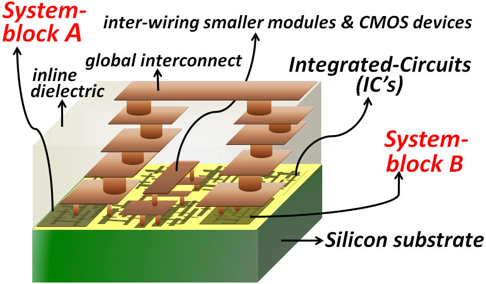 | Figure 7. Cartoon schematic illustrating the typical interconnection adopted nowadays between two system-blocks in a monolithically integrated CPU or SOC. Micro-meters long and bulky interconnects are required to procure these interconnections. System-block A is shown inter-wired to System-block B with long bulky layers of interconnects and vias |
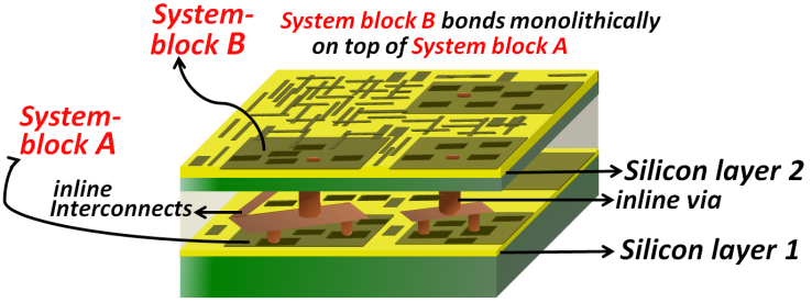 | Figure 8. Cartoon schematic illustrating our new “system on top of system” approach in which System block B of “Figure 7” connects directly on top of System block A of same figure with miniscule nanoscale-size interconnects |
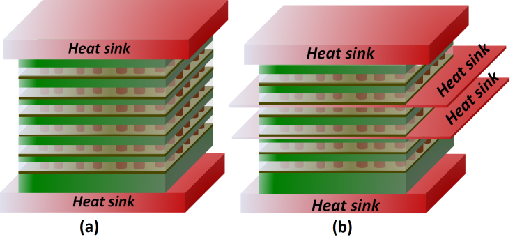 | Figure 9. (a) Schematic illustrating the vertical stacking of plurality of ultra-thinned sheets of Silicon layers on top of one another in high-rise skyscraper-style architecture. (b) High thermally conducting materials/films (e. g. Graphene) can be sandwiched between the Silicon floors for a more effective heat management |
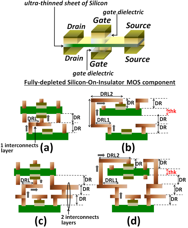 | Figure 10. Schematic illustrating the double-sided MOS transistor structure. (a) Schematic illustrating the vertical inter-wiring between double-sided transistors in different Silicon layers when one layer of interconnects inter-wires the CMOS devices in a same Silicon layer. (b) A comparative schematic to (a) illustrating the similar inter-wiring being used in today’s more conventional approach to monolithic 3D integration and that utilizes TSV’s. (c) Schematic illustrating same vertical inter-wiring to (a) between double-sided transistors but when two layers of interconnects inter-wire the CMOS devices in a same Silicon layer. (b) A comparative schematic to (b) illustrating the similar inter-wiring being used in today’s more conventional approach to monolithic 3D integration using TSV’s |
3.1. Comparative Benchmarks
3.1.1. Impediment to Switching Speed from Interconnects
- Simulations were carried on both approaches to monolithic 3D integration that the “Figure 10” shows while also considering that high-current 18mA large-periphery CMOS devices drive the vertical interconnect to the Gates of transistors above them. These simulations are shown in “Figure 11”. Equations estimating the time delay from interconnects as these were defined in section 2.1.1 were utilized. The design-rules for metal-1 10nm node from Table 1 were used in simulations but with dimension H taken as design-rule for the length of isolation trenches in the direction of the devices Gate widths (WG), and with dimension
 in the “Figure 2” pointing vertically instead of pointing into the computer-screen or paper. H was set to 60nm. A design-rule of the vertical height for each interconnects or metals layer (DR) was set to 50nm. The other dimensions in “Figure 10” were each set such: DRL=15nm, thk=20nm (this is the thickness of the Silicon sheet), DRL1=25nm and DRL2=35nm. The Celmor value was 20fF in all simulations. All calculated values for ξ were close or higher than unity.
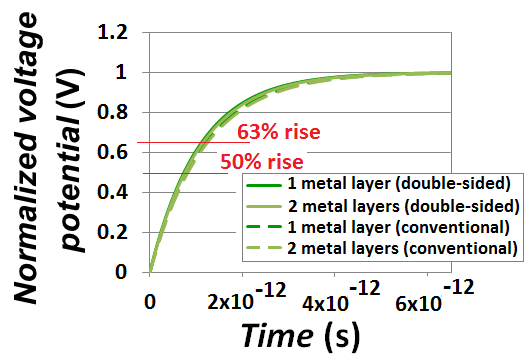 | Figure 11. Comparative RC-delay from interconnects in today’s conventional approach to monolithic 3D integration that uses TSV’s and in our newly proposed approach that utilizes double-sided CMOS components  |
 and
and  , the propagation time delays from interconnects close to what the metal-1 interconnects in today’s conventional 2D IC’s are delivering (similar to what “Figure 4” showed). “Figure 11” implies that a
 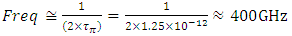 can be delivered through such vertical inter-wiring between transistors provided that the driving transistors can deliver such same or higher speed, and that the intense heat that will consequently generate from such extreme speed is manageable.
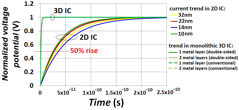 | Figure 12. Simulated time delays due to interconnected in today’s 2D IC’s and in next generation 3D IC’  |
3.1.2. Effect from Parasitic Coupling
- Our proposed novel approach to monolithic 3D integration may raise concerns and constraints on the effects from signal coupling to victim lines. This is because of the much more rapid rise time of the electric signals through its vertical inline interconnects that inter-wire the transistors and modules in different Silicon layers. This effect was simulated on the four separate vertical interconnections to the Gate of a transistor that the “Figure 10” shows. “Figure 13” shows representative schematics depicting this coupling and the active regions in these vertical interconnections that are most prone to it.
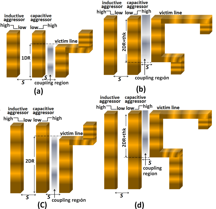 | Figure 13. Representative schematics illustrating the effect from coupling due to an aggressing line on the interconnections to Gate that the “Figure 10” shows when larger DR and T are utilized |
 away from same victim line acts as an inductive aggressor on it. However because magnetic flux that induces in spacing: S, which has nanoscale-size dimension, and along the lengths of the vertical interconnections in monolithic 3D IC’s that also have nanoscale-size lengths, is substantially small compared to the relatively large capacitance caused by the same nanoscale-sized value of S (equaling 29nm), the effect from the inductive aggressing line was neglected in our simulations of coupling. Furthermore, because highest capacitive coupling incurs in portion of an interconnect victim line that is in closer proximity to an aggressing line our simulations were oversimplified to assume that it is only this portion in a victim line that gets coupled. These regions are clearly shown in the “Figure 13” for the four separate vertical interconnections to the Gate of a transistor that the “Figure 10” shows.Capacitive coupling was estimated following the model in [17] through which the magnitude of peak potential
  that couples to victim line was defined as
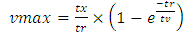 | (13) |
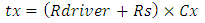 wherein Cx is the equivalent capacitance of the effective coupling regions that the “Figure 13” shows, and Rs is the resistance in portion of victim line that connects to a transistor Drain and in which the effect from capacitive coupling was neglected in simulations (because it is sufficiently weak). tv is computed following [17].Simulations were performed for the four separate vertical interconnections from Drain-to-Gate that the “Figure 10” shows. “Figure 14” shows the simulated couplings on victim lines for the four interconnects configurations of “Figure 13”. Key findings are that all couplings are sufficiently low (< 0.25V).
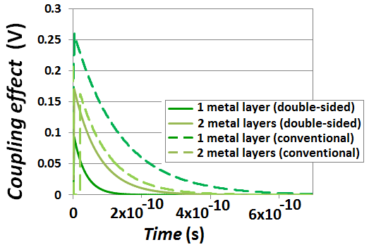 | Figure 14. Capacitive coupling’s from a vertically conducting aggressing line on a paralleled victim line that connects the Drain of one transistor to Gate of another |
3.1.3. Power Efficiency
3.1.3.1. Dynamic Power
- “Figure 15” shows simulated data for the dynamic powers that would dissipate in the CMOS transistors channel and in the interconnects of monolithically integrated 3D IC’s due to the switching cycle of one CMOS. Simulation followed the models specified in Sections 2.1.1, 2.2.1, and the corresponding design-rules for metal-1 10nm node as these were specified in Section 3.1.1 and in Table 1.
 | Figure 15. CMOS dynamic power simulations for monolithically integrated 3D IC’s, and in today’s conventional 2D IC’s when CMOS drive a global interconnect. Both have same capacitive loads at the interconnect line termination.  |
 and
and  ). Also shown in same figure are the typical dynamic powers that dissipate, due to the switching cycle of one CMOS, in today’s conventional 10nm node 2D IC’s when CMOS drives a global interconnect. Both powers were simulated for a range of switching frequency (Freq) varying from 5GHz to 50GHz.Apparently when a low capacitive load exists at the beginning of interconnect lines
  , the monolithic 3D IC appears to ensure a dynamic power loss per CMOS at 28GHz equaling that in today’s conventional 2D IC’s when switched at low 8GHz. Furthermore, even at a high 50GHz CMOS speed the dynamic loss per CMOS in monolithic 3D IC was simulated to be only 0.2mW higher than at 8GHz in same 3D IC. The 50GHz dynamic loss per CMOS in conventional 2D IC was in comparison 0.8mW higher than at 8GHz in same 2D IC. This very drastic enhancement in the dynamic power dissipation is attributed to the substantial reduction of the magnitudes for Clump from what its values are in the global interconnects of today’s conventional 2D IC’s.
3.1.3.2. Standby Power
- “Figure 16” shows simulated data for the standby power in monolithically integrated 3D IC’s following the model for the transistor leakage (or Off-state) current in double-sided FD-SOI MOS as this was covered in [14]. The main equations of this model were also described in the Section 2.2.2. Model for the short-channel VT used in simulations was also described in [14]. As figure shows, the biasing of secondary Gate has strong impact on pronouncedly shifting this device VT in either direction. This effect is due to the strong electro-static coupling between the two Gates in this device; this was described in full details in [14]. Such independent biasing for secondary Gate can enable the device to be software-programed to have lowest VT and highest drive current when it is On, and swap instantly to have far higher VT and lowest standby power when it is switched Off. Simulations in “Figure 16” clearly demonstrate how through positively back-biasing the secondary Gate in a double-sided FD-SOI n-MOSFET that incorporates long Gate length (LG) equaling 90nm its VT value drops excessively low equaling 125mV (shown in black circle with mark A), same as the VT value in transistor incorporating far shorter Gate length equaling 10nm but which secondary Gate is unbiased (shown in orange circle with mark B).
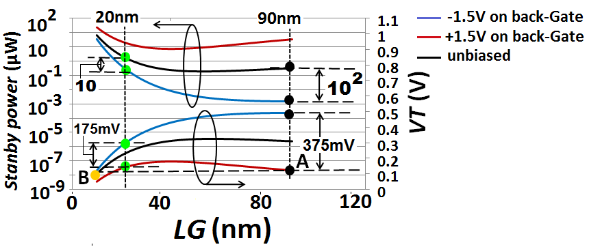 | Figure 16. Simulations of Standby power and VT in an n-MOSFET FD-SOI transistor as it can be incorporated in our proposed monolithically integrated 3D IC’s (It is assumed that p-MOSFET will be balanced to have similar magnitude for Standby power). (tox = 0.65nm on both Gates; tsi = 10nm; WG = 0.5µm; Gate work-function: φg =0.8V; lateral dimension of HALO is 8nm; HALO doping is 20×1018 cm-3; body doping is 20×1017 cm-3; VD = 0.8V) |
4. Conclusions
- Analytic simulations based on established models for interconnects and transistor devices demonstrated that monolithically integrated three-dimensional integrated-circuits do offer dramatic enhancements to the speed and power-efficiency for next generation CPU’s and SOC’s. These enhancements were shown to be driven by an extensive reduction in the size of interconnects that are used to inter-wire the transistors and their system blocks in today’s Central-Processing-Units (CPU’s) and Systems-On-Chips (SOC’s). The large and bulky interconnects in today’s CPU’s and SOC’s were also demonstrated to be the major cause to impeding the switching speed and increasing the dissipative powers in these monolithic systems. It was further shown that it is these global interconnects that caused the clock speed in today’s CPU’s to saturate around 8GHz when overclocked.Our novel approach to monolithic 3D integration enables a virtually infinite amount of transistors to be monolithically integrated and stacked on top of one another and it will revive the steady pace of Moore’s law. It is also manufacturable with standard CMOS-like processes that use none other than “good old” Silicon and copper interconnects which are still the only few materials proven to date of having a flexible capability to manufacture large-scale integrated electronics. These processes were described in our Patent application US15/731,051 [18].The Standby power in the transistors can reduce by more than one or two orders of magnitude and their performance can improve drastically through an effective use of secondary Gates in these transistors. These dramatic improvements in device performance and suppression of standby power were shown realizable through back-biasing the secondary Gate in fully-depleted MOS transistors. This suggests a direction to relax the Gate pitch in future technologies and back-bias secondary Gates of FD-SOI MOS to boost performance and suppress standby power. Furthermore, since transistors will also integrate vertically, the Gate width of transistors can be increased to enable higher drive currents while the continuous denser integration of transistors can still be realizable through the continuous vertical stacking of transistors on top of one another.
ACKNOWLEDGEMENTS
- The author would like to thank the staff at Solidi Technologies for their support throughout this project.