-
Paper Information
- Paper Submission
-
Journal Information
- About This Journal
- Editorial Board
- Current Issue
- Archive
- Author Guidelines
- Contact Us
Microelectronics and Solid State Electronics
p-ISSN: 2324-643X e-ISSN: 2324-6456
2018; 6(1): 1-10
doi:10.5923/j.msse.20180601.01

Pulsed Bias and Its Effect on Heat-induced Degradation in GaN-based HEMTs that Incorporate Barriers Having High Aluminum Content
 Abstract
 Reference
 Full-Text PDF
 Full-text HTML
Ahmad Houssam Tarakji
Device organization unit, Solidi Technologies, Sacramento, United States of America
Correspondence to: Ahmad Houssam Tarakji, Device organization unit, Solidi Technologies, Sacramento, United States of America.
| Email: |  |
Copyright © 2018 The Author(s). Published by Scientific & Academic Publishing.
This work is licensed under the Creative Commons Attribution International License (CC BY).
http://creativecommons.org/licenses/by/4.0/

We report on the pulsed bias operations of GaN-based High-Electron-Mobility-Transistors (HEMTs) that incorporate epitaxial barriers having high Aluminum content. These devices are known to suffer from irreversible permanent degradation of their currents at Drain biases that are higher than 12-15V. This is limiting their use nowadays in most practical applications. In this work we demonstrate with modelling and experimental data that excessive self-heating caused by LO phonons in the GaN 2DEG channel is major contributor to this degradation. We also demonstrate that one approach to alleviate this excessive self-heating is by weakening the lateral field in 2DEG channel between Drain and Source. We finally demonstrate the mechanism that limits the application of higher Drain biases to be caused by combined effect from this intense self-heating and an added bias-induced strain that appears to further strain the already strained and intensely heated GaN 2DEG and accelerate the increase of traps density in GaN. Our data further suggest that epitaxial barrier and its AlN-spacer remained virtually unaffected after prolonged application of high 45V DC bias and that most epitaxial damage appears to confine in GaN, particularly under the access region between Gate and Drain and at the Drain side in the channel under the Gate where both electric-field and the self-heating are highest. An accurate Physics-based model for these HEMTs was also developed and its simulations agreed with our experimental measurements and aided us to formulate these conclusions.
Keywords: HEMT, pulsed bias, AlInN, AlN
Cite this paper: Ahmad Houssam Tarakji, Pulsed Bias and Its Effect on Heat-induced Degradation in GaN-based HEMTs that Incorporate Barriers Having High Aluminum Content, Microelectronics and Solid State Electronics , Vol. 6 No. 1, 2018, pp. 1-10. doi: 10.5923/j.msse.20180601.01.
Article Outline
1. Introduction
- Recent advancements in the growth of Nitride semiconductor epitaxies have only recently started allowing depositions of Nitride epitaxies incorporating high Aluminum content that possess high spontaneous polarizations into a Gallium Nitride (GaN) 2-Dimensional-Electron-Gas (2DEG). Record high sheet carrier concentrations
 close to 2.7-3.2×1013cm-2 and current-densities as high as 2-3A/mm are continuously and routinely reported nowadays from High-Electron-Mobility-Transistors (HEMTs) that incorporate these epitaxies. These epitaxies are either grown by incorporating 2-4 nm strained Aluminum Nitride (AlN) barriers atop GaN [1], or by growing these barriers thicker with traces of Indium incorporated into them to alleviate the strain. The Indium molar fractions can be anywhere between 5-15%. Both approaches were reported to produce excellent spontaneous polarizations into the GaN 2DEG channel with highest device current-densities [2-5]. Yet one obstacle is still impeding the use of these devices in the applications that require them to operate at high bias. It is the resulting intense self-heating from which these devices are known to suffer and that confines in their GaN 2DEG and degrades their electric performance irreversibly [6-13]. This phenomenon is characteristic to HEMT devices that have high Aluminum substance in their epitaxial barriers and high corresponding sheet carrier concentrations [6-13]. It manifests itself with a pronounced increase of the self-heating in their channel which irreversibly degrades their electric performance. This intense self-heating was attributed to the continuous emissions of Longitudinal-Optic (LO) phonons when high fields are applied to the GaN 2DEG channel between the Drain and Source. LO phonons are lattice vibrations that are quantized at specific wavelengths and caused by electrons emitting a corresponding energy they lose from scattering [6-13]. The time its takes an LO phonon to convert to other phonon modes that can more easily sink out the heat from the GaN 2DEG channel is measured with the phonon-lidetime. This is inherintly high in HEMTs that have high
  [6-13]. Though prior works pointed to the longer phonon-lifetime in AlInN-based HEMTs as possible mechanism that is permanently degrading their electric performance none demonstrated tangibly how the phonon-lifetime modulates the self-heating in these devices and none explained why the high applied fields between Drain and Source drastically intensify this self-heating and accelerate the irreversible degradation of these devices. The work in [9] pointed to thermal breakdown in contacts and to a Gate sinking to result from this intense self-heating. The work in [10] reported on a degraded channel conductance in these devices due to high applied DC bias to their Drain. It explained this degradation to an increase of the traps density in GaN 2DEG from hot-electrons. Neither work did however provide a quantitative measure on the contribution from LO phonons to this intense self-heating and nor on the potentials to improve the electric performance of these devices with pulsed bias. Other work reported on the capability of these devices to operate at temperatures as high as 1300⁰K when high thermal conductive substrates are incorporated [14]. Same work showed that current-densities as high as 3A/mm can be reached when these devices are cooled down to cryogenic temperatures. These are highest current-densities ever reported from a solid-state transistor which therefore implies that if these transistors are integrated in miniaturized radar units for next generation fighter-jets they can deliver highest RF powers that will enable detection of enemy jets at distances three times larger than what today’s state-of-the-art AlGaN/GaN HEMTs can deliver (given that the typical current-densities in today’s AlGaN/GaN HEMTs are close 1A/mm). Such dramatic enhancement in performance can however come only if this irreversible permanent degradation of the electric performance of these devices is adequately tackled. In this work we demonstrate for the first time that heat that generates in GaN 2DEG due to electron scattering with other than LO phonons may be suppressed when low duty-cycle pulsed-bias is utilized whereas the intense heat that generates due to electron scattering with LO phonons tends to remain confined in GaN 2DEG and can still limit the electric performance of these devices. Aided with accurate simulations that precisely duplicated our devices Current-Voltage characteristics (I-V’s) we extracted their corresponding channel temperatures at which their irreversible permanent degradations started to incur. We observed that these devices degraded irreversibly as the intense heating in their GaN 2DEG channel approached the thermal limits for bulk GaN (~ 2500⁰K). We also observed that inverse-piezoelectric effect can accelerate the damage to an already intensely heated GaN 2DEG when higher potentials are applied between Drain and Gate. We further demonstrate with simulations that one approach to alleviating this intense self-heating caused by electron scattering with LO phonons and that confines in the GaN 2DEG channel is by weakening the lateral field in this channel.
 2. Device Structure
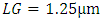
- The epitaxial layers for HEMT devices were grown in Aixtron 2000HT reactor using standard precursors on insulating 4H-SiC substrates. A 0.3µm thick AlN buffer was grown first over SiC substrates. This was then followed with growth of 1.5µm thick semi-insulating GaN. Growth of Ultra-thin (2-3nm) AlN spacer and ~9nm thick AlInN barrier were carried next. Purpose of this AlN spacer is to alleviate the channel scattering at the GaN interface. The Aluminum molar composition in AlInN barrier was targeted around 90%. A 20Ǻ AlN cap layer was finally deposited with pulsed-Atomic-Layer-Epitaxy (PALE) to crown the AlInN barrier. This AlN cap was demonstrated to further stretch the Polarization effects and alleviate the surface Breakdown [15]. Devices were fabricated with relatively long 1.25µm Gates
 that still enabled a short-channel device performance, and with wide Gate-to-Source and Gate-to-Drain openings
  . Reasons for these wider openings are to weaken the lateral field between Drain and Source and to lessen the phonon-induced self-heating. The Gate width was same on all fabricated devices equaling 8×50µm. The Gate-to-Source openings were 2µm wide and the Gate-to-Drain openings were between 6µm and 9µm wide in different devices. Total of 12 devices were used in this study from which 3 had an
  . The measured data in this manuscript figures represent typical performances in devices having same
  . I-V’s of all devices having a same
  were matched within a 5-15% error. Ti/Al/Ti/Au multilayer Ohmic contacts were deposited by e-beam evaporation followed by a 30s rapid thermal annealing at 850°C in N2 atmosphere. A Ni/Au bilayer was deposited for the Gate electrode followed by a
  thick PECVD Si3N4 layer for device passivation. 4 other similar devices incorporating plain AlN barriers that are close to 2-2.5nm thick were also fabricated with PALE. The average measured Hall Mobility (µh) and sheet carrier density (nsh) on all devices were close to 1300cm2/(V.s) and 2.85×1013cm-2 respectively. “Figure 1” shows cartoon schematics for the fabricated device structures.
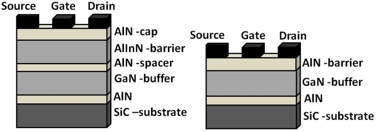 | Figure 1. Cartoon schematics of our HEMTs that incorporate plain AlN barriers and those that incorporate thicker barriers containing close to 10% Indium |
3. Device Model and Results
- Though the devices having plain AlN barriers exhibited a similar trend to self-heating as the devices that incorporated AlInN barriers with I0% Indium, in order not to crowd our figures we show in this work the electric characteristics and the self-heating in the devices that incorporated AlInN barriers only. The conclusions are however similar for the devices incorporating plain AlN barriers.
3.1. Device Model
- The short-channel saturation-velocity model for field-effect transistors [16] was used for simulating the I-V curves of devices. These simulations accounted for the dependence of electron saturation-velocity and electron channel mobility on the channel temperature. We modelled the dependence of mobility on channel temperature due to electron scattering with LO phonons
 following the Bose-Einstein distribution function in [9]. This is since it is well known and it was specifically demonstrated in [9, 17] that the temperature rise in GaN 2DEG due to excited LO phonons follows a Boltzmann-like distribution which consequently causes
  to follow a same distribution with
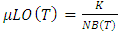 | (1) |
 is the Bose-Einstein distribution function as it was defined in [9] and K is a constant. This mobility adds in parallel to another mobility
  that results from other mechanisms of electron scattering.
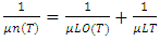
 includes scattering’s that are less temperature-dependant such as those due to interface roughness, defects, piezoelectric scattering and electron-electron scattering. The expression for
  from [9, 17] is
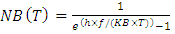 | (2) |
 | (3) |
 is the desired value for
  at 300⁰K. The model for device short-channel current conforms to the equation,
 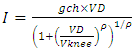 | (4) |
 is the voltage to drain,
  is a fitting parameter that models the transition of current from its linear-mode to saturation
  , and gch is its extrinsic linear channel conductance expressed with
 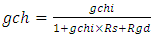 | (5) |
 | (6) |
 is the 2DEG sheet charge estimated with:
 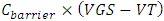 . VT is the device threshold-voltage,
  is the capacitance per unit-area of device barrier and
  is the potential applied between Gate and Source. Rs and
  are the extrinsic Source and Drain resistances of the device that are function of temperature. WG and LG are the device Gate width and Gate length respectively. q is the electron charge unit
  . Estimate for Rs and
  are
are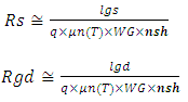 | (7) |
 and
and  are the Gate-to-Source and Gate-to-Drain access regions. Estimate of the Vknee in short-channel field-effect devices is
 | (8) |
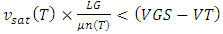 | (9) |
 ,
,  , and a low field room temperature
  and
and  . Therefore the short-channel criterion of equation (9) is met at 300⁰K for VGS = +1.5V. When this criterion is not met,
 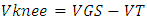 and the saturation device current of equation (4) becomes
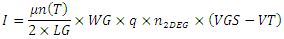 The rise of channel temperature due to electron scattering with LO phonons
  is modelled to follow similar Bose-Einstein distribution function as our modelling of
  . This is since some electrons do emit more LO phonons from this scattering to further energize the lattice vibrations and increase the scattering and the self-heating for same bias. The number of electrons that emit in LO mode from this scattering is known to follow a similar statistical distribution as that of equation (2) [9, 17]. This continuous process of emissions and increased scattering latches a self-sustained feedback that thrusts higher emission rate for LO phonons and causes consequent higher rate of heat build-up in GaN 2DEG which slows its diffusion to substrate and forces most of it to confine instead in the GaN 2DEG channel and raises this channel temperature. The Bose-Einstein distribution function captures the average number of excited LO phonons for given applied field and an initial temperature
  . Electrons do still scatter due to other scattering mechanisms (with other than LO phonons) and these also increase this channel temperature
  due to their Ohmic conduction in it. The total temperature in 2DEG channel at given applied bias is therefore
 | (12) |
 that is less sensitive to the thermal conductance of substrate and to device thermal package because it tends to confine in the GaN 2DEG channel even when SiC substrates are used,
  does depend highly on the thermal conductance of substrate and/or on the device thermal package. It is modelled with
 | (13) |
 is the equivalent thermal resistance between hot GaN 2DEG and coldest reference in device structure.
  is the thermal time-constant for heat rise in GaN 2DEG and
  is the time duration of the applied potential to Drain. When device operates with a pulsed bias
  , both pulsed and time-averaged heating caused by electron scattering with other than LO phonons can be suppressed. The pulsed heating can be suppressed with
  while a low
  and a low duty-cycle suppress the time-averaged heating. Heating that is however caused due to electron scattering with LO phonons is more difficult to suppress with pulsed bias as it tends to confine in GaN 2DEG during the
  . Both initial temperature
  prior to an electric field is pulsed and the number of excited LO phonons due to this field contribute together to an increase of
  . Therefore,
  may also be reduced to lesser extent with very low duty-cycle since
  will reduce and resets closer to 300⁰K at beginning of each pulse following
 is the period of pulsed signal. The Bose-Einstein relation between
  and the total average number of excited LO phonons as it was described in [9, 17] is
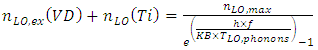 | (14) |
 is extracted from the above equation for the values of
  and
and  .
.  is the average number of LO phonons excited due to an applied field, and
  is the average number of LO phonons at temperature
  and that also follows a Bose-Einstein distribution function described in [9, 17] with
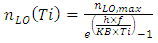 | (15) |
 .
.  is the Boltzmann’s constant
  .
.  is the quantized energy of LO phonons that are stimulated from electrons emitting upon scattering (f corresponds to longer infrared wavelength. We used
  in our simulations).
  in equations (14) and (15) represents the maximum amount of available LO phonons in the volume that is covered by the GaN 2DEG
 .
.  was modelled in [9, 18] with
 | (16) |
 from [9, 18] is
 | (17) |
 is the total length of 2DEG GaN (in our devices
  .
.  is the enclosed volume in GaN Wuritzite unit cell.
 | (18) |
 . An expression for
  can now be estimated [9] with
 | (19) |
 is the distance over which an electron must travel to reach an LO phonon energy equalling
  . It was derived in [9] to be close to
  | (20) |
 that corresponds to an averaged magnitude for electric field
  in entire
  such
such
 is the varying lateral electric-field through
  and
and  is an estimate for the effective-electron mass when an electron reaches
  at high fields and emits energy
  . Its expression is
  when assuming the electron reaches a peak velocity between scatterings that is twice its saturation-velocity (this is since saturation-velocity is the time-averaged velocity). Our model is more accurate than that demonstrated in [9] and it differs from it by accounting to an added contribution to channel temperature due to the Ohmic conduction of electrons that scatter with other than LO phonons and to its transient rise in the channel. It also provides accurate modelling for extrinsic channel transconductance, for short-channel and long-channel
  for device drive current and for its dependence on the channel temperature. It also accounts to the impacts from
  and
and  on the average number of excited LO phonons and on the corresponding shift in channel temperature that these cause.
 , and
, and  were used for simulating the HEMTs having
  and
and  Gate-to-Drain spacing respectively. These were estimated using the nominal
  thermal conductivity of a SiC substrate with oversimplified estimations that mirrored the effects from this substrate thickness
  ,
,  and
and  on
on  Our simulations also used
  . This was taken from simulated estimates for the temperature rise in a GaN 2DEG formed on top of high thermal conductive SiC substrate [19]. We also used
  in all our simulations, and
  .
.3.2. Results from Measurements and Simulations
- Pulsed measurements were carried on all fabricated devices. The Magnitude of the voltage pulse to their Drain (VPulse) was set to rise from 0V and remain constant during time interval:
 . The time between pulses:
  was set to 1s and VPulse increased 1mV after each period
  . The applied potentials to Gates (VGS) were synchronized to VPulse. Unlike in conventional 60Hz curve-tracers that capture effects of averaged self-heating in response to 60Hz sweeps to device terminal, our measurements used the Accent-DIVA-D265 system that sampled magnitudes for the device current at the end of every
  . This permitted the capture of effects from self-heating during each time-interval in which different
  was applied. This consequently mirrored the real-time dynamic response of the currents of devices due to an increasing VPulse. A schematic illustrating the time-dependence of VPulse as it was used in our measurements is shown in “Figure 2”.
 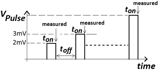 | Figure 2. Schematic illustrating the time-dependence of VPulse |
 and that were biased with
  .
.  was set to 0.61ms in measuring one device (HEMT-A) and to 10µs in measuring the other device (HEMT-B).
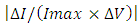
  was 6µm in HEMT-A and 9µm in HEMT-B. To quantify the self-heating in these devices we picked an arbitrary measure from their measured I-V’s using metric:
 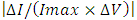 . This captured for given ton and VGS the heat-induced reversible decrease of their saturation-currents
  with the increase of
  relative to the peak value of their saturation-current
  . The self-heating of both devices was also simulated following the model described in previous section. It was observed that their measured I-V’s were fully reversible and recoverable for magnitudes of VPulse below 10.5V for HEMT-A, and below 20V for HEMT-B, and provided that VPulse never exceeded these cut-offs prior on the corresponding device. It was further observed that as
  exceeded these cut-offs (that correspond to the marks B and B’ in “Figure 3a”) the currents of both devices ceased to follow their smooth steady trend that simulations showed and both currents started an unexpected uptick at these cut-offs. The root-cause of these upticks as it will be demonstrated later are caused by continuous shifts of their phonon-lifetime that continuously reduced the self-heating in these devices as
  continued to increase and further degrade their
  . Measurements that extracted their
  as
as  was increasing indicated that a permanent irreversible damage did incur to both devices after VPulse reached its corresponding cut-off on each device.
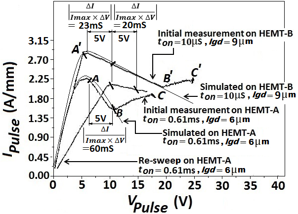 | Figure 3a. Measured and simulated dynamic currents response to VPulse for HEMT-A and for HEMT-B. VGS =1.5V. (Devices that incorporated plain AlN barriers showed a similar trend) |
 | Figure 3b. Measured IGPulse and electrically extracted n2DEG versus VPulse on the corresponding HEMT-A and HEMT-B of “Figure 3a”. (Devices that incorporated plain AlN barriers showed a similar trend) |
 from which a corresponding
  was calculated. These showed clear gradual irreversible degradations after
  reached its corresponding cut-off on each device. After
  reached 10.5V,
  started reducing permanently in HEMT-A, from its initial measured magnitude of
  to a value of
  at
at  .
. started to similarly reduce permanently in HEMT-B after
  reached 20V on this device, from same initial magnitude of
  to
to  at
at  . These values for
  were estimated with
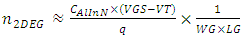 | (21) |
 is the Gate-to-Source capacitance. It was measured with Agilent 4284A C-V meter while
  . “Figure 3b” shows the corresponding measured pulsed Gate leakage currents
  and
and  versus
  for the HEMTs of “Figure 3a”. Apparently no correlation exists in both devices between the onsets of their degraded
  that “figure 3a” shows and the upticks of
  that “Figure 3b” shows. The onsets for their degraded
  in “Figure 3b” however matched precisely the magnitudes for
  in “Figure 3a” at which the currents of both devices started deviating from their expected and simulated trends (corresponding to the marks B and B’ in both figures). We also observe from “Figure 3a” that our measure of the self-heating in devices that metric
 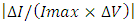 captures is less pronounced in HEMT-B that was pulsed with smaller
  (compared to the larger
 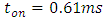 used to measure HEMT-A).
 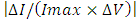 was 60mS for HEMT-A but only 23mS for HEMT-B. A re-sweep (or a second sweep) of VPulse on HEMT-A with
  < 20V and same ton =0.61ms confirmed a clear degraded device performance that manifested itself with reduced peak saturation-current and higher Vknee (the Vknee increased from 5V to 10V). This re-sweep is also shown in “Figure 3a”. This observed irreversible (permanent) increase of the Vknee confirms that substantial damage had incurred to the GaN 2DEG channel below the access region between Drain and Gate. The self-heating on same device however reduced drastically as is demonstrated from the measured
  on same device during this re-sweep (it reduced to 20mS from its 60mS high when the device was initially measured. The cause of this reduction of self-heating after
  degraded is same as what caused the currents of HEMT-A and HEMT-B in same figure to begin increasing once their
  started continuously degrading with increasing
  and is attributed to a reduced phonon-lifetime. A second re-sweep for same range of
  on HEMT-A confirmed same I-V as that of first re-sweep that is shown in “Figure 3a”. This implies that once device degrades at given Drain potential and
  no further degradations incur to device provided that no higher bias gets applied to its Drain. Because the onsets for the irreversible degradations of
  in both devices (that “Figure 3b” shows) incurred as the self-heating of their currents (that “Figure 3a” shows) were continuously and gradually increasing; and because HEMT-A that was measured with larger
  and showed consequent more pronounced self-heating started degrading at lower
  ; and because the
  of both devices did not correlate to the onsets of their degraded
  , we conclude that that the observed degradations of
  in “Figure 3b” are predominantly caused by excessive self-heating that confines in the 2DEG channel of these devices. This conclusion is consistent with findings in [6, 10, 12] that pointed to self-heating and hot electrons in GaN 2DEG as the most likely cause to this irreversible permanent degradation of the electric performance in similar AlInN-based HEMTs.“Figure 4” shows simulated 2DEG channel temperatures for the devices which data were shown in “Figure 3a” and “Figure 3b”. Apparently the 2DEG channel temperature in HEMT-A reached magnitude at mark
  equalling
 . This is close to the thermal limit of Bulk GaN that is close to 2500⁰K. Similarly the 2DEG channel temperature in HEMT-B reached magnitude at mark B’ equalling:
  . This is also substantially high given that
  was effectively suppressed due to much lower
  (compared to
  in measuring HEMT-A). This suppression is because the thermal transient rise of channel temperature that is caused by heat that generates due to electron scattering with other than LO phonons is suppressible with high thermally conductive substrates and/or an efficient thermal device package.The simulated temperatures in “Figure 4” are deemed accurate as they enabled same model to duplicate following their trend with
  the measured I-V’s of both HEMTs that “Figure 3a” shows. It is further observed from “Figure 4” that
  of HEMT-B is noticeably lower than that of HEMT-A for same range of
  . We believe that it is the wider
  in HEMT-B and not the lower
  while measuring this device that exerted stronger influence on lowering its
  This is because a larger
  weakens the lateral field between Drain and Source and consequently increases the length over which an electron must travel to reach its quantized energy for LO emission (following equation (20)). This in turn reduces
  and consequently lowers the channel temperature due to electron scattering with LO phonons (following equations (19) and (14)). This conclusion is being further supported with the additional simulations in “Figure 5” that show the trends for
  and that for the currents of devices versus
  for different values of
  and with low
  that effectively suppressed
  . These simulations demonstrated clearly that larger values of
  cause weaker lateral fields in
  between Drain and Source and suppress
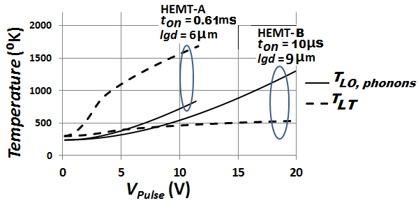 | Figure 4. Simulated  and and  versus versus  for the HEMT-A and HEMT-B of “Figure 3a” and “Figure 3b”. (VGS =1.5V) for the HEMT-A and HEMT-B of “Figure 3a” and “Figure 3b”. (VGS =1.5V) |
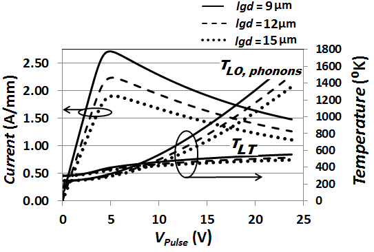 | Figure 5. Simulated  and corresponding device currents versus and corresponding device currents versus  for different values of for different values of  |
 that “Figure 3b” shows for HEMT-A and HEMT-B can be expected to cause currents of both devices to decrease, the very exact opposite was observed in “Figure 3a”. We will demonstrate that these increases of currents in both devices are caused by a continuing reduction of their hot phonon-lifetime as these devices continued to degrade with the continuous increase of
  . It was established in [6] that
  modulate the phonon-lifetime but no work demonstrated tangibly that same phonon-lifetime modulates the self-heating in GaN 2DEG and alter the devices I-V’s. To demonstrating this we swept
  at
at  and
and  on two additional new devices that were not measured prior.
  was swept up to 40V on one device degrading it while reducing its
  to 6.8×1012 cm-2 and its
  to 0.75A/mm from an initial 2.25A/mm, and it was similarly swept up to 45V on the other device degrading it while reducing its
  to 5.5×1012 cm-2 and its
  to 0.86A/mm from same initial magnitude. Both devices had an initial
  equalling 1.9×1013 cm-2 prior to degrading. After these initial sweeps that irreversibly degraded both devices they were both swept again with same
  and
and  and with
  not exceeding 27V on either. These re-sweeps are shown in “Figure 6”. “Figure 6” also shows the I-V’s for HEMT-A from “Figure 3a” before and after this device degraded. All currents in “Figure 6” were normalized to their
  . Most apparent from “Figure 6” is that the self-heating in these devices that we quantified with
  decreased at first with decreasing
  and re-increased again with continuous decrease of
  . The
. The  reduced from 60mS in HEMT-A prior to degrading, to 20mS after
  degraded irreversibly on same device, to 4mS in new device which
  degraded more, and re-increased again to 16mS in other new device which
  degraded even more. Such unusual trend can only be explained with that of the phonon-lifetime that follows exact same non-linear shifts with varying
  . That is what actually alleviated the self-heating in the devices of “Figure 3a” once their
  started degrading. “Figure 6” also shows that the permanent shifts in
  that incurred to devices are substantial and inversely proportional to the decrease of their
  after they degraded from higher applied
  .
.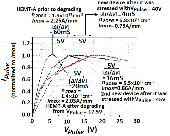 | Figure 6. Measured I-V’s on different devices having different  and different degrees of defects in their GaN. and different degrees of defects in their GaN.   |
 versus
  correlates perfectly to that of the phonon-lifetime. The phonon-lifetime
  in “Figure 7” was fitted following its analytic model in [6] and for the estimate of resonant
 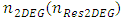 that was extracted from the measurements of “Figure 6”.
  is the GaN 2DEG carrier concentration at which the frequency of LO phonons approaches that of hot electrons and the phonon-lifetime reaches minima. From our measured data in “Figure 6” this closely corresponds to lowest
 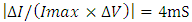 which corresponds to the device having an
 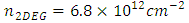 . This therefore makes
  for our processed devices close to this value. Work in [6] had attempted to correlate the currents drop in AlInN-based HEMTs after their
  degraded to their phonon-lifetime after degradation but have obtained a weak and a deluded correlation. This is because the phonon-lifetime correlates to the channel self-heating and not to the degree of current drop after degradation incurs; currents do re-increase after degrading as it was specifically shown in our “Figure 3a”. “Figure 8” shows the simulated trends for the channel temperatures of the devices in “Figure 6” with increasing
  . The measured 2 new devices that were stressed with far higher
  reaching 40V and 45V had very close
  values after they degraded (0.75 and 0.86A/mm). This consequently caused the 2nd measured new device which
  degraded most and that has higher corresponding rate of decrease of its current with increase of
  , in agreement with its phonon-lifetime in “Figure 7”, to have higher channel temperature at
  close or equal to 20-25V. The
  on the other hand of HEMT-A after this device degraded remained relatively high (2.03A/mm) and given that its phonon-lifetime in ‘Figure 7” collapsed substantially after this device degraded to become same or close to that of the 2nd measured new device, its channel temperature was considerably higher due to its much higher current. Same device had highest
  before degrading and highest phonon-lifetime. It did consequently show higher channel temperature for same range of
  as after it degraded.
 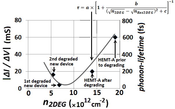 | Figure 7. Phonon-lifetime from [6], and the self-heating assessments for the devices in “Figure 6”.  |
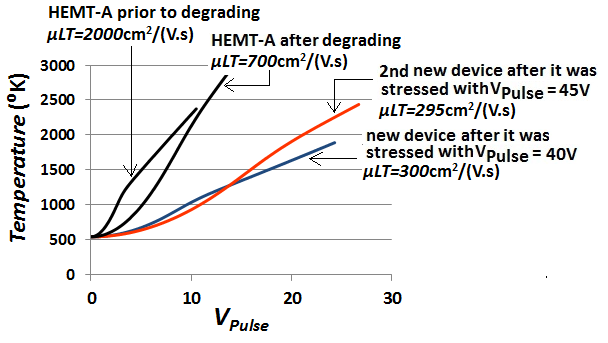 | Figure 8. Simulated total channel temperatures  in HEMT-A before and after it degraded, and in the measured 2 new devices which I-V’s are also shown in “Figure 6” in HEMT-A before and after it degraded, and in the measured 2 new devices which I-V’s are also shown in “Figure 6” |
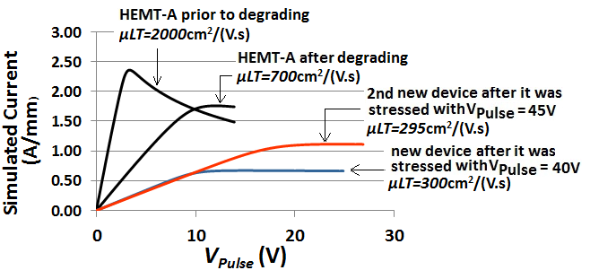 | Figure 9. Simulated device currents for the devices in “Figure 6” |
 | (22) |
 were calculated from equation (21). These mobility’s are shown in “Figure 10”. Their observed increase with increasing
  is due to gradual screen-out of impurities in GaN 2DEG with higher
  . Their decrease on the other hand at higher
  is caused by interface roughness scattering as the electron wave-functions shift toward the interface [20]. The observed collapse of mobility over the entire range of
  after device degraded indicates clearly that substantial damage incurred to the GaN 2DEG as a result. This is consistent with the substantial shifts of the
  ’s that “Figure 6” shows after devices degraded. It is further observed from “Figure 10” that the onset, or the Cutoff magnitude for
  , at which electron scattering with the interface roughness starts predominating is same for both mobility’s and is close to
  . This suggests that no apparent severe damage incurred to AlN spacer, neither from the 45V DC, and that most damage is localized in the GaN. Comparative TLM measurements on same device before and after it degraded confirmed same contact resistance close to 0.7Ω.mm implying therefore that no damage incurred to metal contacts either. We believe that excess self-heating due to electron scattering with LO phonons which confined in the GaN 2DEG damaged the GaN and lowered the device current and phonon-lifetime substantially before any excessive heating was able to diffuse outside the GaN 2DEG and damage the metal contacts.
 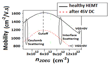 | Figure 10. Calculated mobility’s of 2DEG GaN before and after device degraded permanently from application of a 45V DC.  |
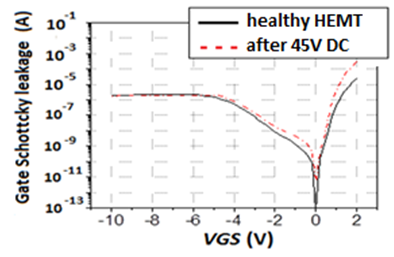 | Figure 11. Measured device Gate leakage currents before and after device degraded permanently from application of 45V DC |
 , and hence, lower duty-cycles on the device performance. For this we defined metric
  as the maximum
  that can be applied to the Drain of device for given
  and
and  before it starts degrading (e. g. for devices in “Figure 3a”
  are 10.5V and 20V for HEMT-A and HEMT-B respectively). Results are shown in “Figure 12”. All measurements were performed on new devices that were not measured prior. Though lower values for
  for same
  are expected to increase
  due to the noticeable reduction of self-heating, the exact opposite is observed from “Figure 12”. The
  did actually reduce.
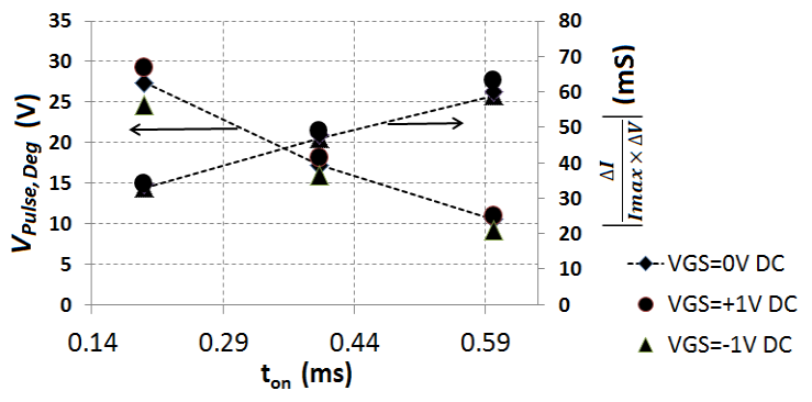 | Figure 12. Measured  versus versus  for different values of for different values of  |
 were applied and this inverse-piezoelectric effect had apparently contributed to accelerating the crystallographic damage to an already excessively heated GaN. Though such strain is known to store mostly in the epitaxial barriers of GaN-based HEMTs, the much thinner AlInN barriers of our devices (~9nm compared to the typical 20-35nm barriers in conventional AlGaN/GaN HEMTs) can cause considerable strain to transfer to the GaN film below it.
4. Conclusions
- We demonstrated that excess self-heating in GaN 2DEG is major contributor to the pronounced irreversible device degradation of GaN-based HEMTs that incorporate barriers having high Aluminum content. We showed that most induced damage causing this degradation appears to confine to the GaN and most pronouncedly under the access region between Gate and Drain and at the Drain side in the channel under the Gate where both electric-field and self-heating are highest. We showed that this induced damage to GaN kicks as the channel temperature approaches the known thermal limits of bulk GaN (~ 2500⁰K). We further showed that inverse-piezoelectric effect can further accelerate this damage to GaN when higher potentials are applied to Drain and that wider Gate-to-Drain spacing’s can suppress the portion of self-heating in GaN 2DEG that is caused by electron scattering with LO phonons. We also demonstrated that by operating the devices with pulsed bias the self-heating caused by electron scattering with other than LO phonons can be effectively suppressed while the portion of self-heating due to electrons scattering with LO phonons is more difficult to suppress as it tends to confine in the GaN 2DEG even when SiC substrates are used. Further studies are required to assess the impacts from further reducing the
 on
on  in devices incorporating different substrate materials; as
  reduces deeper below the micro-second range higher thermal conductive substrates such as Diamond may be capable to further reduce
  even during
  .
. ACKNOWLEDGEMENTS
- The author would like to thank the technical staff at Solidi technologies for their help and support, and to acknowledge the contribution from Prof. Asif Khan with the University of South Carolina for his help on initiating this research and its funding.